PDF 原檔:報告_野村_半導體測試產業_20260724_original.pdf
圖片清單(已驗證 2026-07-26)
lib/ 嵌圖的唯一真相來源。本份共抽出 270 張圖,屬超大型 anchor report;本清單為「範圍性驗證」:只逐張 Read 了產業章節(第 1–3329 行)中規劃嵌入 lib 的候選圖,以及各公司章節由 ingest 執行者現場驗證的圖。清單未涵蓋全部 270 張——日後要嵌本份其他圖號,須依
ingest_steps.mdStep 2.5 現場補驗(ls -la看 size + 逐張 Read),不可照 trimmed 引用順序猜。
| 檔名 | size | 分類 | 親眼所見內容 |
|---|---|---|---|
報告_野村_半導體測試產業_20260724_007.png |
60KB | 真資料圖 | Fig.6 CPO 四段 insertion 流程示意:PIC / EIC 晶圓各自晶圓級測試 → HB 並加矽載板 → EPIC 晶圓級測試 → 切割並貼 receptacle/FAU → OE 單顆級/封裝級測試(標紅字 and/or?)→ 上基板與 ASIC 併排的模組/系統級測試 |
報告_野村_半導體測試產業_20260724_008.png |
72KB | 真資料圖 | Fig.7 CPO insertion 潛在供應商對照表:列 Venue / Process / ATE-Instruments / Prober / Probe card / FT-SLT Handler / Socket,欄為 Insertion 1–4;Insertion 1-2 在 Foundry、3-4 在 OSAT;探針卡欄出現 FormFactor?、MPI/FormFactor?、MPI?;handler 欄 Chroma/Ficontec?、Hon 與 Chroma (ELS);socket 欄 WinWay?/WinWay |
報告_野村_半導體測試產業_20260724_026.png |
119KB | 真資料圖 | Fig.28 Multichip Module Yield vs. Single Die Yield 折線圖:橫軸每模組 die 數 1–20,三條曲線為 99% / 95% / 90% die yield;圖上文字框註「at 90% die yield, a 10-die module has less than 35% final yield」;右側配一顆標 FAIL 的 die 導致整個模組被紅叉打掉的示意 |
報告_野村_半導體測試產業_20260724_064.png |
160KB | 真資料圖 | Fig.67 CP/FT 測試介面與設備四合一示意:左上探針卡結構(main board PCB / relay board / relay connector / probe unit 對 LSI wafer)、左下 IC 測試座結構(test socket / contact probe / tester contact pin / tester contact connector)、右上 tester + wafer prober + test head 與 performance board / spring-type contact pins / probe card / wafer / stage、右下 tester 搭 prober(探針卡對晶圓)與 tester 搭 handler(packages 對 test socket)對比 |
報告_野村_半導體測試產業_20260724_075.png |
27KB | 真資料圖 | Fig.78 pitch 區間與對應測試介面方案:橫軸 pitch 標 50 / 80 / 100 / 350 / 800 µm;MEMS 探針卡色帶落在最細 pitch 端(約 50 µm 以下延伸至 ~75 µm),cantilever(peripheral pad)與 VPC 色帶落在約 80 µm 以上;虛線左標 wafer-level (probe card)、右標 package-level (socket);WLCSP 小色帶在 100 µm 附近,pogo pin 與 elastomer 色帶落在 350 µm 以上 |
報告_野村_半導體測試產業_20260724_013.png |
12KB | 真資料圖 | Fig.15 NVIDIA AI GPU 邏輯製造成本結構堆疊柱圖:Hopper / Blackwell / Rubin 三根,區塊為 Testing(紅,極薄一層)/ Fabrication(灰)/ CoWoS(白框),Rubin 的 Fabrication 佔比明顯低於前兩代、CoWoS 佔比放大 |
報告_野村_半導體測試產業_20260724_048.png |
21KB | 真資料圖 | Fig.50 全球探針卡營收 2019–2030 堆疊柱圖(USDmn,縱軸 0–5,000):2019 約 1,500 逐年成長至 2030 約 4,500;每根柱由下往上分 epoxy/cantilever(紅)、vertical probe card(灰)、MEMS probe card(白框,佔最大部分)、其他先進探針卡(淺色頂層) |
報告_野村_半導體測試產業_20260724_086.png |
68KB | 真資料圖 | Fig.90 JEDEC 三種 tray 工程圖(帶 NOMURA 浮水印):左為現行標準 tray 的 plan view / front view 與 L.SIDE view 標註尺寸,中、右分別為 TYPICAL TRAY BX 與 TRAY CX 的 top and long side views 尺寸圖 |
報告_野村_半導體測試產業_20260724_090.png |
283KB | 真資料圖 | Fig.94 Hon Precision「Active Thermal Control (ATC) Roadmap」(公司版權標示):Dual-temp(25~150°C)列 ATC3.3 (1KW) 2020、ATC3.5 (2KW) 2022〔H series & B series〕、ATC3.6 (3KW) 2025〔B series & R series〕、ATC3.7 (6KW) 2026〔F series〕、ATC3.8 (10KW) 於 2027–2028;中間 Power Density 帶標 30 → 60 → 120 → 130 → 180 → 210 W/cm²;Tri-temp(-80~180°C)列 ATC5.5 (4KW) 2025、ATC5.6 (5.5KW) 2027、ATC5.7 (10KW) 2028 |
報告_野村_半導體測試產業_20260724_092.png |
41KB | 真資料圖 | Fig.97 測試座典型結構剖面圖:上圖標示 socket 本體與 spring loaded floating guide plate、DUT 位於上方、黃色 pogo pin 陣列;下圖為施加下壓力(紅色箭頭)後 DUT 壓入接觸的狀態 |
報告_野村_半導體測試產業_20260724_099.png |
94KB | 真資料圖 | Fig.104 同軸測試座結構四格圖:左為 Smiths Interconnect 針組剖面標 P G S G,中上為 profile 剖面標 air gap (dielectrics) / isolation / top housing / metal housing / GND pin / retainer 與 50 ohm impedance for HF pins,中下為 Yokowo 結構標 polyimide tube / metal block / 50 Ohm Air Gap / pin plate / DUT board,右為 COHU 的 DUT 與 PC Board 之間針組立體圖 |
報告_野村_半導體測試產業_20260724_104.png |
53KB | 真資料圖 | Fig.109 CPO 測試 Insertion 1-4 四階段流程示意(PIC/EIC 單面 → EPIC 雙面 → die-level / OE package-level → 模組/系統級)〔旺矽章節,執行者驗證〕 |
報告_野村_半導體測試產業_20260724_110.png |
573KB | 真資料圖 | Fig.115 MPI Probe Card 全產品線圖:CPC(Pitch 40µm 以上邏輯/7µm 以上 Display Driver)、OSPREY (FW)(Pitch 40µm 以上、小 pad)、KESTREL (MW)(Pitch 70µm 以上、低作用力高針數)、EVS/FCB(Pitch 80µm 以上、高 CCC)四大產品線,對應 Display Driver / MCU / Automotive / Multimedia Communication / PMIC / ASIC / AP / MPU / FPGA / CPU-GPU 應用色塊,下方標 COF-COG、Wire-Bond、Soldering Bumps、Cu-Pillar Bumps、CoWoS 各封裝對應製程節點(3nm-55nm) |
報告_野村_半導體測試產業_20260724_124.png |
45KB | 真資料圖 | Fig.133 先進封裝測試四大挑戰:Ultra Large Package(>100×100mm²)、High Pin Count(>20K pin)、High-Speed Testing(>224Gbps)、High Heat Density(>4,000W)〔穎崴章節,執行者驗證〕 |
報告_野村_半導體測試產業_20260724_132.png |
73KB | 真資料圖 | Fig.142 CPO Insertion 1-4 流程與潛在供應商分工表,Socket 欄在 Insertion 3、4 標示 WinWay〔穎崴章節,執行者驗證〕 |
報告_野村_半導體測試產業_20260724_139.png |
42KB | 真資料圖 | Fig.150 穎崴年度營收趨勢 2023-2028F(TWDmn)長條圖疊 CAGR 折線(46% → 69%)〔穎崴章節,執行者驗證〕 |
報告_野村_半導體測試產業_20260724_149.png |
13KB | 真資料圖 | Fig.164 穎崴 socket 產能長條圖(set/month,千套):2025 約 2 → 1H26 約 3.3 → 2H26 約 4.2 → 1H27 約 7.2 → 2H27 約 8.0 |
報告_野村_半導體測試產業_20260724_163.png |
— | 真資料圖 | 鴻勁產品線圖(handler / ATC / SLK / cold plate)〔鴻勁章節,執行者驗證〕 |
報告_野村_半導體測試產業_20260724_178.png |
— | 真資料圖 | 鴻勁 ATC 世代路線圖(與 _090.png 同一張 Fig.94 內容)〔鴻勁章節,執行者驗證〕 |
報告_野村_半導體測試產業_20260724_196.png |
— | 真資料圖 | 鴻勁全球據點地圖(美國/德國/中國子公司)〔鴻勁章節,執行者驗證〕 |
報告_野村_半導體測試產業_20260724_250.png |
169KB | 真資料圖 | 致茂 CPO Test Solutions 產品線圖:上排流程 Photonics IC (PIC) → EPIC Wafer/Die (EIC+PIC) → Light Engine (Optical Engine) → External Laser Light Source → CPO Switch;下方兩個方案框「PIC Wafer Test Solution:586XX Series(Optical Test / Electrical Test / Reliability Test & WAT)」與「Light Engine & CPO Automation Test Solution:587XX Series、5860X Series、Laser Source(Light Engine O/E Test、CPO Switch Test、Laser Reliability Test、Laser Source for testing)」,多台機型標 NEW |
報告_野村_半導體測試產業_20260724_254.png |
228KB | 真資料圖 | SST(固態變壓器)電源架構圖:AC → SST 模組 → ±400V/800V DC,標示致茂 61800-100、62450D-2000HL、63224A-1200 機型〔致茂章節,執行者驗證〕 |
報告_野村_半導體測試產業_20260724_255.png |
146KB | 真資料圖 | 致茂 AI 伺服器電源測試方案總覽(PSU/BBU、再生電網模擬器 61800/61860HF、雙向 DC Source 62000D 系列、ATS Model 8000、DC 電子負載 63700H/63200A/63202A)〔致茂章節,執行者驗證〕 |
報告_野村_半導體測試產業_20260724_101.png |
217KB | 真資料圖 | Fig.106 測試介面板在測試流程中的位置:左「WAFER LEVEL TESTING — Probe Cards & Tester Components」由上而下 ⓿PIB: Probe Card Interface Board(*)、❶PCB、❷MLO: Multi-Layer Organic、❸Ceramic Plates、❹Contact Probes;右「FINAL TESTING — Final Test Components」由上而下 ❶DIB: Device Interface Board、❸Socket、❹Pogo Pins |
原始內容
ANCHOR REPORT
Global Markets Research 24 July 2026
Advanced Semi Testing
Chip upgrade; testing ahead
Our team has been positive on the semiconductor testing sector since 4Q25, based on our view that: 1) the value of back-end processes as a portion of chip manufacturing costs is increasing in the AI chip era, 2) the streamlining of leading players and spillover effect should benefit overall supply chain players. In this report, we extend our coverage from OSATs to test interface and equipment makers in Taiwan, as they are key enablers in the chip testing process, work as gatekeepers and ensure fewer failures in later stages. We also notice that key vendors command vital strategic value in an industry-wide supply-constrained environment. We maintain our perspective outlined in our most recent sector view (end-June) that we haven't reached AI cycle peak, initiate coverage of MPI, WinWay, Hon Precision, and resume coverage of Chroma, all with Buy ratings.
Key themes and analysis of this report:
- Our understanding of CPO testing flow and potential suppliers ·
- Analysis of testing content in GPU by generation ·
- A natural rise in testing process sophistication along with advanced packaging ·
- Upgrade trend of test hardware to cope with stringent requirements ·
- Observation on test hardware market and related peers ·
- Comparison of major Taiwanese test hardware players ·
Research Analysts
Semiconductor
Vivian Yang - NITB
vivian.yang@nomura.com +886(2) 21769970
Eric Chen, CFA - NITB eric.chen@nomura.com +886(2) 21769965
Aaron Jeng, CFA - NITB
aaron.jeng@nomura.com +886(2) 21769962
Production Complete: 2026-07-23 20:41 UTC
EQUITY: TECHNOLOGY
Advanced Semi Testing
EQUITY: TECHNOLOGY
Chip upgrade; testing ahead
Buy on testing process sophistication, spec upgrade, share gain/order overflow, and supply constraints
In a nutshell, testing is now in the driver's seat
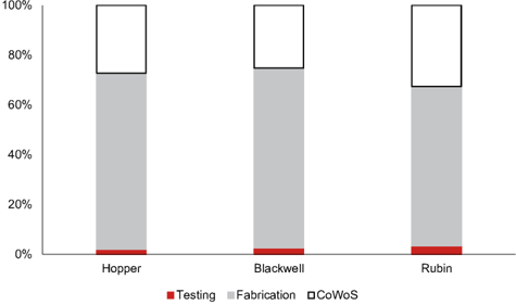
Our team has been positive on the semiconductor OSAT sector since 4Q25 (when we upgraded ASE [3711 TT, Buy] ), on our view that: 1) the value of back-end processing as a portion of chip manufacturing costs continues to rise along with advanced packaging; 2) the streamlining of leading players and spillover effect is likely benefiting overall supply chain players. We further upgraded KYEC (2449 TT, Buy) in Mar-26 following product mix optimization and margin expansions for both the companies. As devices become more complex, testing duration will naturally extend; and, if we take nVidia's (NVDA US, Not rated) AI GPUs as an example, and index the final test (FT) time of Hopper to 1, we estimate 4x for Blackwell and ~7x for Rubin. For system-level test (SLT), if we set Hopper to 1, we estimate 1.5x for Blackwell's SLT time and 2.5x for Rubin's. For burn-in test (BIT), we estimate the test time to likely double from Blackwell to Rubin as well. The extended testing times should be reflected as increased testing content in the cost structure; furthermore, considering the higher hourly rates, we estimate the testing content costs (defined as the sum of FT, BIT and SLT) in nVidia Rubin could rise to 3.3% of the total cost vs. 2.5% for Blackwell and 1.9% for Hopper , leveraging our supply chain analysis (Fig. 15 ).
Complexity of testing processes - from advanced packaging and additional insertions; necessary test hardware upgrades to address testing challenges
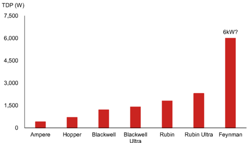
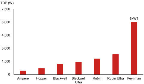
Advanced packaging is driving testing complexity as well, given that: 1) as mentioned, with devices becoming more complex, the testing duration will naturally extend; 2) testing challenges to cope with new packaging trends such as larger package size, high pin count, and fine pitches, etc (Fig. 25 ); 3) power and thermal management is becoming increasingly important for surging chip TDP (Fig. 26 ), and notably, if GPU-on-GPU stacking comes through (we likely estimate in Feynman, see report ), and; 4) more highend PCB/interposer materials are used for ultra-high speed signal transmission (see report for PCB material upgrade trend). We observe the following emerging trends in the testing process: 1) increasing efforts around chip probing (the 'shifting-left' trend to ensure KGD [known good die]), 2) additional insertions to be added to the existing IC testing flow such as BIT and SLT, following extreme user cases such as AI/HPC, and higher requirements to address multi-core coherency, and higher-speed interfaces, etc. The chip testing process needs to be optimized to cope with advanced packaging technologies, and it is necessary to upgrade test hardware such as test equipment and interface as well. Beyond standard specification and material upgrades, we anticipate growing adoption of MEMS probes in probe cards , enhanced thermal/high-speed and high-current capabilities in sockets , and improved tray sizing with thermal management systems in handlers - all driving increased customization requirements.
CPO still in early stages; but substantial opportunities beyond
TSMC (2330 TT, Buy) first introduced the concept of Compact Universal Photonic Engine (COUPE) in 2021. It then debuted COUPE based on hybrid bonding to directly bond electric IC (EIC) and photonic (PIC) together in 2023. At the North America Technology Symposium in 2026, TSMC announced it would bring the world's first 200G micro-ring modulator (MRM) with COUPE into production in 2026, adding to further scale up to a 400G modulator with multiple wavelengths and multi-row fiber array units (FAUs) by 2030. TSMC believes co-packaged optics (CPO) with COUPE on substrate provide 4x power efficiency and 10x latency reduction vs. copper wire, and COUPE on interposer could further enhance performance to 10x power efficiency and 20x latency reduction. Two separate dies (EIC and PIC) comprise the important parts of optical

Research Analysts
Semiconductor
Vivian Yang - NITB vivian.yang@nomura.com
+886(2) 21769970
Eric Chen, CFA - NITB eric.chen@nomura.com +886(2) 21769965
Aaron Jeng, CFA - NITB aaron.jeng@nomura.com +886(2) 21769962
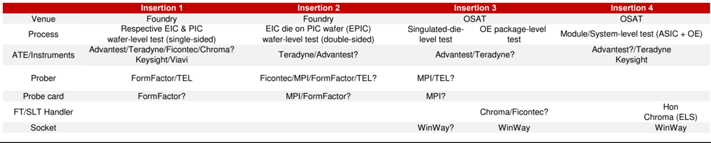
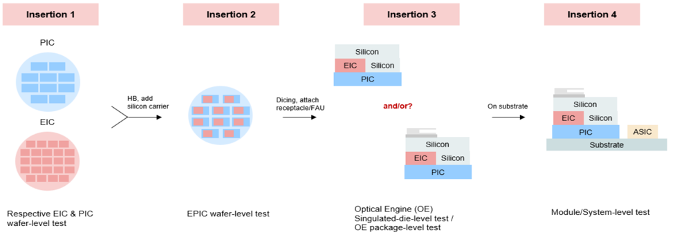
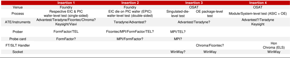
engines (OE), and the optical engines will then be put on the same interposer or substrate with the ASIC (application-specific integrated IC). The optical engine (OE) will need to go through a series of testing at both component level and module/system level to ensure that it can successfully communicate with the ASIC that sits next to it (usually are switch chips, at current development status). As well, the system as a whole requires additional testing. Our understanding of CPO testing insertion is as follows and as shown in Fig. 6 : Insertion 1 is PIC and EIC single-sided wafer-level test; Insertion 2 is double-sided wafer-level test after hybrid bonding; Insertion 3 may include two optical engine (OE)level testing steps after singulation - before and after packaging (attach FAU [fiber array unit]/receptacle/structural reinforcements), and Insertion 4 is the module-level test after the optical engine is mounted on the substrate. While final testing flows and vendor selection could vary by customer, we provide potential candidates for CPO insertions in Fig. 18 .
Stock calls: remain positive on testing supply chain players in our coverage
In this report, we extend our coverage from OSATs to test interface and equipment makers in Taiwan, as we believe they are key enablers in the chip testing process, to work as gatekeepers and ensure fewer failures in later stages. We also notice that vendors command vital strategic value in an industry-wide supply-constrained environment, and they have better pricing power than before. We believe that testing process sophistication, spec/content upgrades, share gain and order overflow from AI ripple effect, and supply constraints should elevate testing supply chain vendors to a pivotal seat. We keep our view from our latest sector view (end-June) that we haven't reached AI cycle peak , initiate coverage of MPI (6223 TT) , WinWay (6515 TT) , Hon Precision (7769 TT) , and resume coverage of Chroma (2360 TT) , all with Buy ratings. We also reiterate Buy on ASE and KYEC . Excluding innovative products still in the incubation stage, these companies already posses substantial project pipelines serving a diverse range of AI chip customers, providing strong order visibility for the next several years (judging from their capacity expansion plans).
Key risks to our investment theme
Major risks include: 1) hyperscalers' capex outlook and comments on AI; 2) an overall slowdown in AI demand along with disappointing monetization progress; 3) a deceleration in new product migration and upgrade cycles, limiting value content growth, and; 4) delays or reductions in capacity expansion plans.
Fig. 1: Stocks for action
| Company | Ticker | Rating | Market cap (USDmn) | Target price (LCY) | Target price (LCY) | Last close (LCY) | Upside / |
|---|---|---|---|---|---|---|---|
| Company | Ticker | Rating | Market cap (USDmn) | New | Old | ( as of 22 July 2026) | Downside |
| ASE | 3711 TT | Buy | 90,585 | 730 | 730 | 656 | 11% |
| Hon Precision | 7769 TT | Buy | 35,597 | 11,100 | Initiation | 6,405 | 73% |
| Chroma | 2360 TT | Buy | 27,912 | 2,845 | Resumption | 2,125 | 34% |
| MPI | 6223 TT | Buy | 18,159 | 8,000 | Initiation | 6,000 | 33% |
| KYEC | 2449 TT | Buy | 11,142 | 390 | 390 | 295 | 32% |
| WinWay | 6515 TT | Buy | 7,235 | 8,315 | Initiation | 6,500 | 28% |
Company description:
ASE
The world's largest outsourced semiconductor assembly and test (OSAT) vendor
Hon Precision
FT/SLT handler provider with 70-80% FT and 20-30% SLT
Chroma
Power test (~50% of parent) and semi/photonic test (~45%) equipment maker
MPI
Leading probe card supplier with 70% of total revenue; rest from testing equipment
KYEC
World's top 10 outsourced semiconductor assembly and test (OSAT) firm
WinWay
Leading test interface suppliers with combined 70% of total revenue from sockets and probe cards
Note: Priced as of 22 July 2026.
Source: Bloomberg Finance L.P., Nomura estimates
Fig. 2: Semi test sector valuation comparison
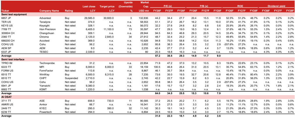
| Last close | Target price | Upside (Downside) | Market Cap. | P/B (x) | P/B (x) | P/B (x) | ROE | ROE | ROE | Dividend yield | Dividend yield | Dividend yield | ||||||
|---|---|---|---|---|---|---|---|---|---|---|---|---|---|---|---|---|---|---|
| Ticker | Company Name | Rating | LCY | LCY | % | USD mn | FY26F | FY27F | FY28F | FY26F | FY27F | FY28F | FY26F | FY27F | FY28F | FY26F | FY27F | FY28F |
| Semi test equipment | ||||||||||||||||||
| 6857 JP | Advantest | Buy | 29,585.0 | 30,600.0 | 3 | 132,836 | 44.2 | 34.4 | 27.7 | 20.4 | 15.5 | 11.9 | 52.5% | 51.2% | 48.7% | 0.2% | 0.2% | 0.2% |
| TER US | Teradyne | Not rated | 374.0 | n.a. | n.a. | 58,553 | 51.1 | 37.2 | 26.7 | 16.2 | 13.1 | 10.0 | 37.5% | 41.7% | 41.9% | 0.1% | 0.1% | 0.2% |
| KEYS US | Keysight | Not rated | 328.1 | n.a. | n.a. | 56,072 | 32.2 | 27.6 | 24.6 | 8.2 | 6.8 | 5.6 | 25.9% | 26.4% | 26.1% | 0.0% | 0.0% | 0.0% |
| 7769 TT | Hon Precision | Buy | 6,405.0 | 11,100.0 | 73 | 35,597 | 47.7 | 29.3 | 19.0 | 16.3 | 12.4 | 9.1 | 37.6% | 48.1% | 55.3% | 1.5% | 2.4% | 3.7% |
| 300604 CH | Changchuan | Not rated | 309.1 | n.a. | n.a. | 28,944 | 94.5 | 64.3 | 46.8 | 29.3 | 20.5 | 14.5 | 33.4% | 34.7% | 33.7% | 0.1% | 0.2% | 0.2% |
| 2360 TT | Chroma | Buy | 2,125.0 | 2,845.0 | 34 | 27,912 | 48.7 | 32.4 | 25.2 | 21.3 | 15.7 | 12.3 | 49.8% | 55.8% | 54.6% | 1.4% | 2.2% | 2.8% |
| 688200 CH | Accotest | Not rated | 369.0 | n.a. | n.a. | 10,926 | 94.8 | 75.0 | 58.8 | 14.2 | 13.4 | 11.3 | 16.2% | 17.8% | 19.1% | 0.3% | 0.4% | 0.6% |
| COHU US | Cohu | Not rated | 56.2 | n.a. | n.a. | 2,652 | 95.8 | 38.3 | 26.4 | 3.5 | 3.2 | 2.9 | -207.6% | 27.2% | n.a. | n.a. | n.a. | n.a. |
| AEM SP | AEM | Not rated | 9.0 | n.a. | n.a. | 2,235 | 42.4 | 27.7 | 21.0 | 5.2 | 4.4 | 3.7 | 13.0% | 16.8% | 18.9% | 0.6% | 0.9% | 1.2% |
| 6337 JP | TESEC | Not rated | 2,339.0 | n.a. | n.a. | 80 | 20.3 | 18.8 | 16.3 | n.a. | n.a. | n.a. | n.a. | n.a. | n.a. | 4.3% | 4.3% | 4.3% |
| Average | 57.2 | 38.5 | 29.3 | 14.9 | 11.7 | 9.0 | ||||||||||||
| Semi test interface | ||||||||||||||||||
| TPRO IM | Technoprobe | Not rated | 31.2 | n.a. | n.a. | 22,854 | 71.9 | 47.2 | 37.0 | 13.2 | 10.5 | 8.3 | 19.6% | 22.6% | 23.1% | 0.0% | 0.1% | 0.2% |
| 6223 TT | MPI | Buy | 6,000.0 | 8,000.0 | 33 | 18,159 | 100.5 | 46.8 | 26.4 | 31.0 | 20.5 | 13.1 | 35.7% | 54.8% | 63.1% | 0.5% | 1.2% | 2.1% |
| FORM US | FormFactor | Not rated | 113.8 | n.a. | n.a. | 8,867 | 46.1 | 35.7 | 39.4 | n.a. | n.a. | n.a. | 15.4% | 18.7% | n.a. | 0.0% | 0.0% | n.a. |
| 6515 TT | WinWay | Buy | 6,500.0 | 8,315.0 | 28 | 7,235 | 73.6 | 35.0 | 19.5 | 32.7 | 20.6 | 12.8 | 46.4% | 71.6% | 80.4% | 1.0% | 2.2% | 3.9% |
| 6510 TT | CHPT | Suspended | 2,710.0 | n.a. | n.a. | 2,745 | 42.2 | 22.7 | 15.9 | 8.2 | 6.3 | n.a. | 20.8% | 31.8% | 56.0% | 1.3% | 2.3% | 2.9% |
| COHU US | Cohu | Not rated | 56.2 | n.a. | n.a. | 2,652 | 95.8 | 38.3 | 26.4 | 3.5 | 3.2 | 2.9 | -207.6% | 27.2% | n.a. | n.a. | n.a. | n.a. |
| 6941 JP | Yamaichi | Not rated | 9,380.0 | n.a. | n.a. | 1,181 | 17.6 | 15.7 | 13.7 | 3.2 | 2.8 | 2.4 | 19.3% | 20.4% | 20.7% | 1.7% | 1.8% | 2.1% |
| 6683 TT | KSMT | Not rated | 1,220.0 | n.a. | n.a. | 1,038 | n.a. | n.a. | n.a. | n.a. | n.a. | n.a. | n.a. | n.a. | n.a. | n.a. | n.a. | n.a. |
| Average | 64.0 | 34.5 | 25.5 | 15.3 | 10.6 | 7.9 | ||||||||||||
| AI OSAT | ||||||||||||||||||
| 3711 TT | ASE | Buy | 656.0 | 730.0 | 11 | 90,585 | 37.2 | 25.5 | 20.2 | 7.1 | 6.2 | 5.5 | 19.7% | 25.6% | 28.6% | 1.9% | 2.8% | 3.5% |
| AMKR US | Amkor | Not rated | 66.7 | n.a. | n.a. | 16,541 | 31.9 | 27.5 | 23.1 | 3.3 | 3.0 | 2.6 | 11.2% | 11.1% | 12.7% | 0.5% | 0.5% | 0.6% |
| 2449 TT | KYEC | Buy | 295.0 | 390.0 | 32 | 11,142 | 30.3 | 19.1 | 14.3 | 5.7 | 4.5 | 3.5 | 21.0% | 26.4% | 27.3% | 0.3% | 0.5% | 0.7% |
| 6239 TT | Powertech | Not rated | 294.0 | n.a. | n.a. | 6,894 | 24.5 | 16.9 | 15.0 | 3.4 | 3.0 | 2.7 | 15.7% | 18.8% | 18.6% | 2.4% | 3.3% | 3.7% |
| Average | 31.0 | 22.3 | 18.1 | 4.9 | 4.2 | 3.6 |
Note: Priced as of 22 July 2026.
Source: Company data, Bloomberg Finance L.P., Nomura estimates
Advanced Semi Testing: Chip upgrade; testing ahead
Our theme in charts
Fig. 3: Core thesis of this report
Multiple designs
Large package
recommendations substrate
PLP
large form factor
Advanced packaging methods innovate every day...
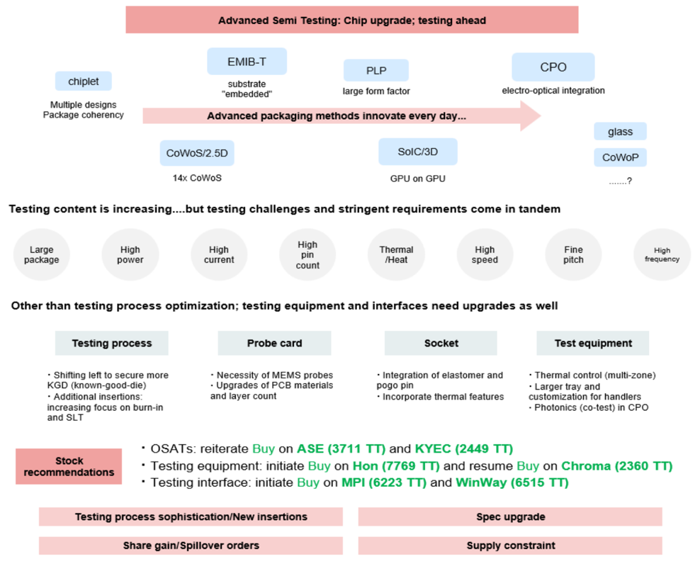
Source: Nomura research
CPO
electro-optical integration
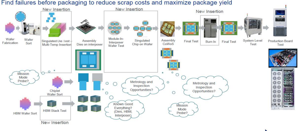
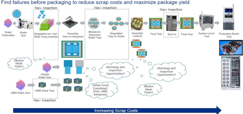
Find failures before packaging to reduce scrap costs and maximize package yield
Fig. 4: Additional testing required in AI era
New Insertion
Wafer
Fabrication
Mission
Model
Probe?
HBM Wafer Sort
Source: Teradyne, Nomura research
Fig. 5: Semiconductor test equipment and interface maker overview
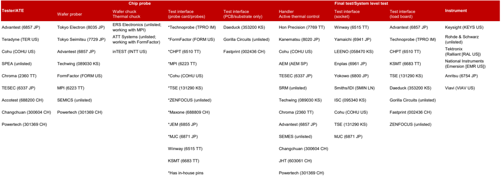
| Chip probe | Chip probe | Chip probe | Final test/System level test | Final test/System level test | Final test/System level test | Final test/System level test | Final test/System level test | |
|---|---|---|---|---|---|---|---|---|
| Tester/ATE | Wafer prober | Wafer chuck Thermal chuck | Test interface (probe card/probes) | Test interface (PCB/substrate only) | Handler Active thermal control | Test interface (socket) | Test interface (load board) | Instrument |
| Advantest (6857 JP) | Tokyo Electron (8035 JP) | ERS Electronics (unlisted; working with MPI) | *Technoprobe (TPRO IM) | Daeduck (353200 KS) | Hon Precision (7769 TT) | Winway (6515 TT) | Advantest (6857 JP) | Keysight (KEYS US) |
| Teradyne (TER US) | Tokyo Seimitsu (7729 JP) | ATT Systems (unlisted; working with FormFactor) | *FormFactor (FORM US) | Gorilla Circuits (unlisted) | Kanematsu (8020 JP) | Yamaichi (6941 JP) | Technoprobe (TPRO IM) | Rohde & Schwarz (unlisted) |
| Cohu (COHU US) | Advantest (6857 JP) | inTEST (INTT US) | *CHPT (6510 TT) | Fastprint (002436 CH) | Cohu (COHU US) | LEENO (058470 KS) | CHPT (6510 TT) | Tektronix (Ralliant [RAL US]) |
| SPEA (unlisted) | Techwing (089030 KS) | *MPI (6223 TT) | AEM (AEM SP) | Enplas (6961 JP) | KSMT (6683 TT) | National Instruments (Emersion [EMR US]) | ||
| Chroma (2360 TT) | FormFactor (FORM US) | *Cohu (COHU US) | TESEC (6337 JP) | Yokowo (6800 JP) | TSE (131290 KS) | Anritsu (6754 JP) | ||
| TESEC (6337 JP) | MPI (6223 TT) | *TSE (131290 KS) | SRM (unlisted) | Smiths/IDI (SMIN LN) | Daeduck (353200 KS) | Viavi (VIAV US) | ||
| Accotest (688200 CH) | SEMICS (unlisted) | *ZENFOCUS (unlisted) | Techwing (089030 KS) | ISC (095340 KS) | Gorilla Circuits (unlisted) | |||
| Changchuan (300604 CH) | Powertech (301369 CH) | *Maxone (688809 CH) | Chroma (2360 TT) | Cohu (COHU US) | Fastprint (002436 CH) | |||
| Powertech (301369 CH) | *JEM (6855 JP) | Advantest (6857 JP) | TSE (131290 KS) | ZENFOCUS (unlisted) | ||||
| *MJC (6871 JP) | SEMES (unlisted) | MJC (6871 JP) | ||||||
| Winway (6515 TT) | Changchuan (300604 CH) | |||||||
| KSMT (6683 TT) | JHT (603061 CH) | |||||||
| *Has in-house pins | Powertech (301369 CH) |
Source: Company data, Nomura research
Fig. 6: CPO insertion flow
EIC
Respective EIC & PIC
wafer-level test
Silicon
EIC Silicon
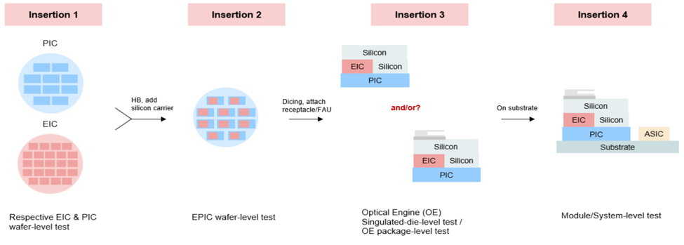
Note: This is a conceptual illustration, not specific to any company or project.
Source: Nomura research
Fig. 7: CPO insertion flow and potential suppliers
| Insertion 1 | Insertion 2 | Insertion 3 | Insertion 3 | Insertion 4 | |
|---|---|---|---|---|---|
| Venue | Foundry | Foundry | OSAT | OSAT | OSAT |
| Process | Respective EIC & PIC wafer-level test (single-sided) | EIC die on PIC wafer (EPIC) wafer-level test (double-sided) | Singulated-die- level test | OE package-level test | Module/System-level test (ASIC + OE) |
| ATE/Instruments | Advantest/Teradyne/Ficontec/Chroma? Keysight/Viavi | Teradyne/Advantest? | Advantest/Teradyne? | Advantest/Teradyne? | Advantest?/Teradyne Keysight |
| Prober | FormFactor/TEL | Ficontec/MPI/FormFactor/TEL? | MPI/TEL? | ||
| Probe card | FormFactor? | MPI/FormFactor? | MPI? | ||
| FT/SLT Handler | Chroma/Ficontec? | Hon Chroma (ELS) | |||
| Socket | WinWay? | WinWay | WinWay |
Source: Nomura research
Fig. 8: Comparison of major global tester and handler makers
| USD mn | Headquarter | Market cap 2025 | revenue | Revenue mix | Revenue mix | 2025 GM | 2025 OPM | 2025 net profit Tester | 2025 net profit Tester | Handler |
|---|---|---|---|---|---|---|---|---|---|---|
| USD mn | Headquarter | Market cap 2025 | revenue | Tester | Handler | 2025 GM | 2025 OPM | Handler | ||
| Chroma ATE (2360 TT) | Taiwan | 24,332.8 | 908.4 | 10-15% | 20-25% | 61.5% | 32.5% | 375.2 | Mature logic/analog | FT 30-40%, SLT 60-70% Mostly logic/analog |
| Advantest (6857 JP) | Japan | 123,945.2 | 6,902.1 | 82% | <5% | 62.4% | 39.7% | 1,927.8 | 80% Logic/Analog 20% Memory | FT, SLT Mostly memory |
| Teradyne (TER US) | US | 50,462.1 | 3,190.0 | 75% | 15% | 58.3% | 22.3% | 632.1 | 80% Logic/Analog 20% Memory | SLT Mostly logic/analog |
| Cohu (COHU US) | US | 2,414.9 | 453.0 | ~40% | ~40% | 43.3% | 0.5% | (10.1) | Mature logic/analog | FT, SLT Mostly logic/analog |
| Hon. Precision (7769 TT) | Taiwan | 33,781.0 | 971.3 | n.a. | c.80% | 56.5% | 49.7% | 396.6 | n.a. | FT 70-80%, SLT 20-30% Mostly logic/analog |
| Kanematsu (8020 JP) | Japan | 2,157.8 | 7,062.3 | n.a. | <5% | 15.7% | 4.4% | 215.8 | n.a. | FT, SLT (from Seiko Epson) Mostly logic/analog |
| TESEC (6337 JP) | Japan | 75.5 | 37.6 | 45% | 36% | 37.8% | 5.7% | 2.0 | Mature logic/analog Discrete | FT (from Yokogawa) Mostly logic/analog |
| Techwing (089030 KS) | South Korea | 1,222.7 | 112.0 | n.a. | 36% | 42.2% | 10.0% | 6.6 | n.a. | FT Mostly memory |
| SEMES (unlisted) | South Korea | n.a. | n.a. | n.a. | n.a. | n.a. | n.a. | n.a. | FT Mostly memory | |
| AEM (AEM SP) | Singapore | 2,137.2 | 305.6 | 30% | 30% | 25.7% | 5.9% | 13.0 | Mature logic/analog | FT, SLT Mostly logic |
| Changchuan (300604 CH) | China | 26,090.7 | 736.2 | c.60% | c.30% | 55.1% | 24.4% | 185.2 | Logic/Analog Discrete | FT, SLT Logic/Analog, Discrete |
| Accotest (688200 CH) | China | 11,034.7 | 187.3 | c.90% | n.a. | 73.8% | 36.5% | 74.6 | Logic/Analog Discrete | n.a. |
| JHT (603061 CH) | China | 3,917.9 | 97.1 | n.a. | c.90% | 52.2% | 30.5% | 24.6 | n.a. | FT, SLT Logic/Analog, Discrete |
| Powertech (301369 CH) | China | 2,233.8 | 49.3 | c.85% | c.85% | 55.7% | -3.1% | 4.7 | Logic/Analog Discrete | FT Logic/Analog, Discrete |
Note: Market cap data as of 17 July 2026.
Source: Company data, Bloomberg Finance LP, Nomura estimates
Insertion 2
Insertion 3
Insertion 4
Active Thermal Control (ATC) Roadmap
TDP (W)
7,500
Fig. 9: Major logic chip products and their testing platforms
B series
R series
F series
| Company | Product | test (FT) | System level test (SLT) | |
|---|---|---|---|---|
| Tester (ATE) | ATC/handler | ATC/handler | ||
| nVidia | AI GPU Consumer GPU CPU | Advantest Advantest Advantest | Hon Hon Hon | Chroma Chroma Chroma |
| AMD | AI GPU Consumer GPU | Advantest Advantest | Hon Hon | Hon Chroma (MI400 series) Hon |
| AI ASIC CPU | Advantest Advantest | Hon Hon | Broadcom: No SLT MediaTek: Hon Chroma | |
| AWS | AI ASIC CPU | Teradyne Advantest | Hon Hon | US vendors Hon (evaluating?) No SLT |
| Microsoft | AI ASIC CPU | TBD? TBD? | TBD? TBD? | TBD? TBD? |
| Meta | AI ASIC | TBD? | TBD? | TBD? |
| Broadcom | Networking | Teradyne, Advantest | Hon | No SLT |
| Tesla/SpaceXAI | AI ASIC | Teradyne | Hon | Hon |
| Intel | CPU | Teradyne | Cohu, Hon? Hon | AEM |
| Apple | Advantest, Teradyne | Hon | ||
| Mobile AP | Hon | |||
| MediaTek Qualcomm | Mobile AP Mobile AP | Advantest Advantest | Hon Hon | Teradyne |
Dual-temp
(25~150°C)
Tri-temp
(-80~180°C)
Source: Hon Precision, Nomura research
Source: Company data, Nomura estimates
Fig. 10: Thermal control becomes more critical along with AI/HPC chip performance advancements
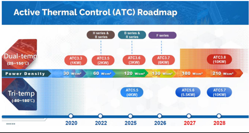
Source: Hon Precision, Nomura research
Fig. 11: TDP of nVidia products
Source: Company data, Nomura estimates
6kW?
Paulanges are Malcalve, bouruales between aujavell lech ologies ale tans ton contes Whele solutions Uvellap lest Halawale die shipped belore Chip Mass proauction
Cantilever (peripheral pad)
Fig. 12: Comparison of major Taiwanese test interface suppliers
MEMS probe card
+
wafer-level (probe card)
| CHPT (6510 TT) | MPI (6223 TT) | WinWay (6515 TT) | KSMT (6683 TT) | ||
|---|---|---|---|---|---|
| Financials | Market cap (USDbn)* | 2.74 | 18.16 | 7.24 | 1.04 |
| 2025 Revenue (TWDmn) | 4,806 | 13,371 | 7,857 | 2,136 | |
| 2025 GM (%) | 55.5% | 55.6% | 45.3% | 46.1% | |
| 2025 OpM (%) | 24.8% | 28.2% | 26.3% | 25.2% | |
| 2025 EPS (TWD) | 30.41 | 33.49 | 46.93 | 15.42 | |
| Probe card | 65.0% | 72.2% | 29.0% | 36.5% | |
| Socket | 56.0% | ||||
| 2025 Product mix | Load board/BIB/SLT board | 25.0% | 61.6% | ||
| Contact element | 11.0% | ||||
| Equipment | 26.1% | ||||
| Others | 10.0% | 1.7% | 4.0% | 2.0% | |
| Probe card PCB | O | ∆ | ∆ | ∆ | |
| Probe card interposer/substrate | O | O | ∆ | ∆ | |
| Product coverage (mfg/design) | Probe head/probe card assembly | O | O | O | ∆ |
| - MEMS probe capability Sockets | O (in-house) | O (in-house) | O (third-party) O | O (third-party) | |
| Load board/BIB/SLT board | O | ∆ | |||
| Probe card PCB/Load board | Capacity to triple in 1Q27 vs. end-25. Fab 3 to ramp in 2028. | In-house PCB fab to ramp in 2H27 | |||
| Capacity | Probe card pins | CPC: ~500kpm VPC: 1,200/2,000 kpm MEMS: 1,000/3,500 kpm in end-2025/26F | |||
| Sockets | Capacity to be more than double in 2026F vs. 2025 | ||||
| Catalysts | AI hype and new project announcements | GPU ramp; key ASIC ramp | Key ASIC ramp; CPO | GPU ramp; key ASIC ramp | project win |
| Risks | AI demand deterioration | No progress in turn-key | CPO & ASIC delay | Key projects delay; profitability headwinds | project loss |
-12m
Test interface
Note: Market cap is as of 22 July 2026.
Source: Company data, Bloomberg, Nomura research
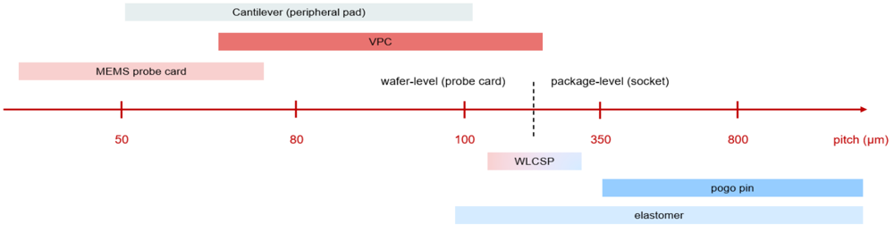
Fig. 13: Typical pitch regimes and corresponding test interface solutions
Pitch ranges are indicative; boundaries between adjacent technologies are transition zones where solutions overlap
Note: This is a conceptual illustration, not specific to any company or project.
Source: Nomura research
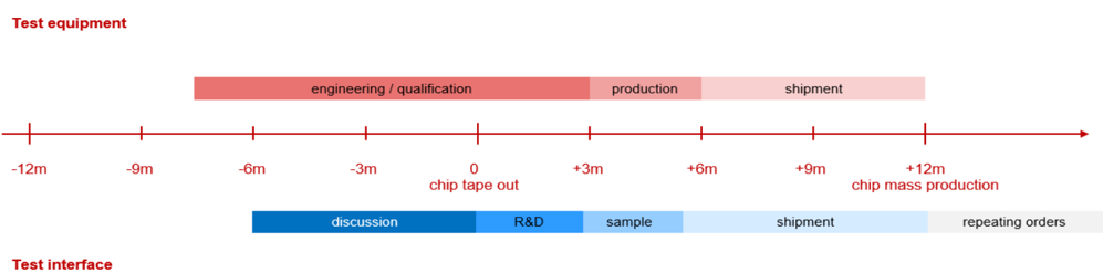
Fig. 14: Timeline of testing equipment and interface preparation
Test hardware are shipped before chip mass production

Note: This is a conceptual illustration, not specific to any company or project. Source: Nomura research
+
shipment
-
100%
80%
60%
40%
20%
0%
vve lematively dooulle oux tom substiale oice lur reyman
10,000
9,000
8,000
7,000
6,000
Fig. 15: Increasing testing content in the logic manufacturing cost of nVidia AI GPUs
3,000
2,000
1,000
Source: Company data, Nomura estimates
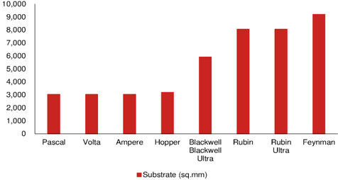
Fig. 16: Key GPUs substrate size is growing We tentatively assume 80x115mm substrate size for Feynman
Pascal
Source: Company data, Nomura estimates
Source: Company data, Nomura estimates
Silicon photonics to lead the next frontier
Increased testing demand from unprecedented testing process flows
SiPh/CPO, due to its advantage of power saving and the natural advantage of longdistance data transmission of optics (vs. copper), will likely be the next big thing in semiconductor advanced packaging area, in our view. nVidia's Ethernet scale-out CPO switch is expected to launch from 2H26E along with the Vera Rubin platform (nVidia's first CPO switch Spectrum-6 was announced to be in full production in Mar-2026 , according to Jensen Huang). While a significant volume ramp-up may not happen in 2026, the complexity of the component and high material/production costs enhances the costs of failure - which is the key driver of testing intensity. In our view, the CPO testing ecosystem is now taking shape and will eventually fully unlock business opportunities for testing players.
TSMC first introduced the concept of Compact Universal Photonic Engine (COUPE) in 2021. It then debuted COUPE based on hybrid bonding to directly bond electric IC (EIC) and photonic (PIC) together in 2023. At the North America Technology Symposium in 2026, TSMC announced it would bring the world's first 200G micro-ring modulator (MRM) with COUPE into production in 2026, adding to further scale up to a 400G modulator with multiple wavelengths and multi-row fiber array units (FAUs) by 2030. TSMC believes copackaged optics (CPO) with COUPE on substrate provide 4x power efficiency and 10x latency reduction vs. copper wire, and COUPE on interposer could further enhance performance to 10x power efficiency and 20x latency reduction.
Two separate dies (EIC and PIC) comprise the important parts of optical engines (OE), and the optical engines will then be put on the same interposer or substrate with the ASIC (application-specific integrated IC). The optical engine (OE) will need to go through a series of testing at both component level and module/system level to ensure it could successfully communicate with the ASIC that sits next to it (usually are switch chips, at current development status). As well, the system as a whole requires additional testing.
The process flow of these CPO components could be split into 4-5 test insertions, depending on the way they are sliced. At every stage, different equipment and test interface will be adopted. Although traditional test insertion still exists in some steps, a brand-new market emerges for testing equipment and interface suppliers, that is, cotesting for optical and electrical signals (i.e., electro-optical test). Also note that either wafer probing or final testing require ATE (automated test equipment) to run a specific testing program designed for the wafer or chip, fueling strong tester demand. Usually a tester compiles a series of instrument cards, but to address severe signal attenuation and optical alignment challenges, external, high-frequency/optical measure instruments will be augmented to standard ATE and probers, ensuring signal integrity and testing fidelity. See more details on testing process and hardware in Key test consumables and equipment within the testing process .
A typical process flow, potential suppliers, and industry dynamics could be as follows:
Insertion 1: Respective EIC & PIC wafer-level test
The first step in the CPO test flow is a separate test for both the EIC and PIC wafers. The insertion is sometimes known as a PIC wafer test only, as EIC wafer test has long been a mature technology. At this stage, PIC and EIC will each require their own probe card and prober. The wafer test at this stage is single-sided (i.e. upper end surface)
Insertion 2: EIC die on PIC wafer's wafer-level test
After running through wafer probing for the two respective wafers, the EIC wafer will be singulated into dies, after which good dies will be stacked onto the PIC wafer through hybrid bonding (making it an EPIC wafer). At this stage, a silicon carrier will also be added. The EPIC wafer will then undergo an electro-optical test. Double-sided wafer level testing needs to be here, during which electrical probing is done from the top side while optical probing is conducted from the bottom side. Many suppliers are developing their resources for this stage given its complexity and it is highly value-added. A specific probe card design would then follow after a decision is made on equipment.
Insertion 3: Optical Engine (OE) singulated-die-level test
Post hybrid-bonding, the stacked PIC-EIC would be singulated to an OE chip. At this stage, whether the OE chip needs to be tested before attaching FAU/receptacle/structural
Insertion 2
Insertion 3
reinforcements remains to be seen, and thus some refer the stage as Insertion 3/3.5 (preand post- packaging). From this stage, a testing insertion will take place in OSATs. Whether a FAU or a receptacle will be attached to the diced OE chip would depend on each vendor's architecture. Thereafter, the entire OE chip will undergo testing. Pre- and post-packaging will have different equipment and test interface, with the former resembling die-level test (more like wafer probe) and the latter more similar to chip-level probing. Usually from this stage, an optical test will be conducted for the top surface while an electrical test will be conducted for the bottom surface. EIC Silicon On substrate
Insertion 4: Module/System-Level Test
PIC
After OEs are tested, good OEs will then be mounted on substrate (or interposer in the future). Here, the OEs will be on the same surface with ASICs, working as a CPO module. This insertion needs to ensure the whole module works smoothly, and smooth communication between ASICs and OEs. After this stage, whether a CPO module would then be put on a larger board for System-Level -Test (SLT) remains to be seen.
In our view, the first two insertions will be conducted/handled by foundries, as it is more like wafer-level process and it incorporates EIC and PIC stacking. From Insertion 3, OSATs can play a role. We believe SPIL (under ASE) could be a major service provider initially, but it's also likely that other OSATs can participate after production volume rampup or when more vendors join the field with new projects.
Although mass production is nearing, our industry channel checks suggest there remains significant uncertainties. The testing process is not determined yet, including but not limited to: 1) a good solution for Insertion 2, given highly demanding requirements for double-sided wafer test; 2) whether to go through both die-level and package-level tests for Insertion 3; and 3) whether SLT is necessary after module-level-test in Insertion 4. Also, even if the process flow is determined, what would be the yield? Apart from the above-mentioned, vendor selection for each stage is another uncertainty, and equipment selections will impact the adoption of test interface.
That said, we believe CPO is a painful yet inevitable shift in semi manufacturing. The unstoppable tide of change will provide a brand-new market for testing suppliers. All participants are pushing to innovate and breakthrough engineering limitations, and once they break through technical bottlenecks, and when the market gradually gets matured, these suppliers could enjoy a new landscape of opportunities, in our view.
Fig. 17 - Fig. 18 illustrate our expected insertion flow and potential supplier candidates.
Fig. 17: CPO insertion flow
Note: This is a conceptual illustration, not specific to any company or project.
Source: Nomura research
Insertion 4
Silicon
EIC Silicon
PIC
ASIC
Substrate
Module/System-level test
Teoung proctooes are muleaslyly complatel along wial compier paunagily
Fig. 18: CPO insertion flow and potential suppliers
Source: Nomura estimates
C4 bump or C2 bump Cavity
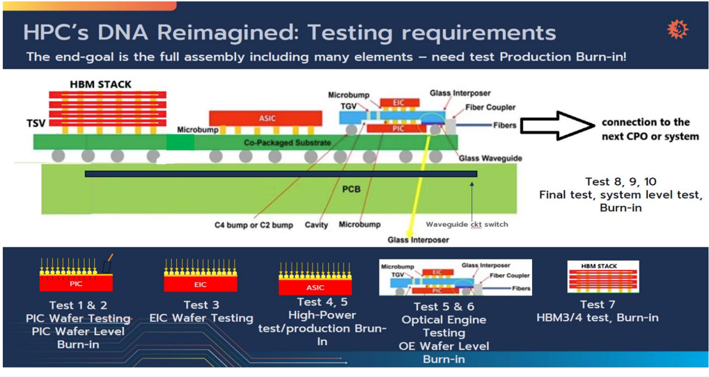
Fig. 19: An example of CPO testing flow
Microbump
Waveguide ckt switch
Glass Interposer
Microbump
TGV
TEIC
Testing processes are increasingly complicated along with complex packaging
Test 5 & 6
Glass Interposer
Fiber Coupler
- Fibers
PIC Wafer Testing
PIC Wafer Level
Source: ASEH, Nomura research
TSV
HBM STACK
Test 7
Is a Key Strategic Component
Traditionall chipmaking
value chain
Packaging Ecosystem
Testing, now much more important than before
80%
Advanced chipmaking
value chain
60%
40%
20%
time to market.
0%
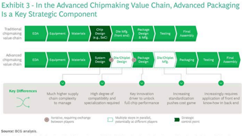
Role of back-end process is playing an increasingly critical role in chip manufacturing for advanced chips
We maintain our view that the role of back-end process (both assembly and testing) is increasingly important within the semi manufacturing process (Fig. 17 - Fig. 18 ); we highlighted that production of AI chips would benefit back-end packing-and-testing process significantly more than that of smartphone chips (a growth driver in the past decade) in our ASE upgrade report in Oct-2025. Sources: Capital IQ, Gartner, 2019 split; BCG analysis.
Materials
Increasing on estabbished
front end co-development
of packaging technology
materials
• Small increase
As devices become more complex, testing duration will naturally extend; and, if we take nVidia's (NVDA US, Not rated) AI GPUs as an example, and index the final test (FT) time of Hopper to 1, we estimate 4x for Blackwell and ~7x for Rubin. For system-level test (SLT), if we set Hopper to 1, we estimate 1.5x for Blackwell's SLT time and 2.5x for Rubin's. For burn-in test (BIT), we estimate the test time to likely double from Blackwell to Rubin as well. The extended testing times should be reflected as increased testing content in the cost structure; furthermore, considering the higher hourly rates, we estimate the testing content costs (defined as the sum of FT, BIT and SLT) in nVidia Rubin could rise to 3.3% of the total cost vs. 2.5% for Blackwell and 1.9% for Hopper , leveraging our supply chain analysis (Fig. 22 ).
Fig. 20: Back-end process is increasing value with advanced packaging
Source: BCG analysis, Nomura research
Fig. 21: BoM share of back-end process will increase along with advanced packaging
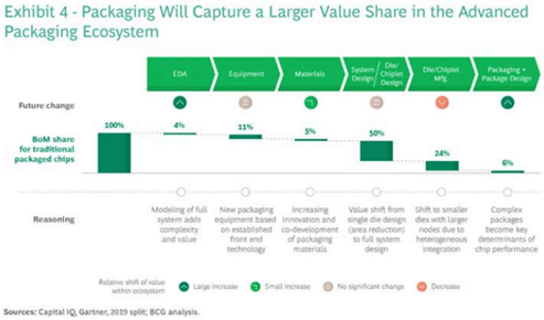
Source: Capital IQ, Gartner, BCG analysis, Nomura research
Fig. 22: Increasing testing content in the logic manufacturing cost of nVidia AI GPUs
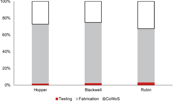
Source: Company data, Nomura estimates
Ole/
System / Chiplet resign Desig
Value shift from single die design
(area reduction)
to full system design
3 No significant change
Die/Chiplet
Mig
Shift to smaller dies with larger
nodes due to heterogeneous
integration
Packaging
Package Design
Complex packages
determinants of become key
chip performance
Dil ullis
2,500
2,000
1,500
1,000
500
120
Advanced packaging drives testing intensity
5Y CAGR: 31%
Advanced packaging is still a small portion of total semi packages, but will grow rapidly
2024
2029E
•High-end Packaging
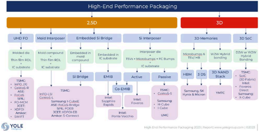
Advanced packaging is driving testing complexity as well, given that: 1) device complexity increase will require a longer testing time; 2) testing challenges to cope with new packaging trends such as larger package size, high pin count, and fine pitches (Fig. 25 ), etc; 3) power and thermal management is increasingly important for surging chip TDP ( Fig. 26 ), and; 4) more high-end PCB/interposer materials are used for ultra-high speed signal transmission (see report for PCB upgrade trend). Advanced packaging technologies such as 2.5D/3D packaging, chiplet architectures, hybrid bonding, and multidie systems will increase interconnect density and complexity significantly. According to Yole's forecasts, the number of high-end performance packages units was just <2% of total IC units in 2024, but it may grow to ~5% of total ICs by 2028E. Given the wellacknowledged physical limit on front-end manufacturing process, we believe advanced packaging will continue to increase its value proportion in semi manufacturing, and subsequently drives testing intensities.
The yield cliff and the criticality of CP KGD in advanced packaging
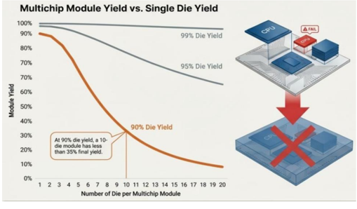
As the semiconductor industry shifts toward advanced packaging and Multichip Modules (MCM), manufacturers face a severe "yield cliff (Fig. 28 )". Because the overall module yield is the cumulative yield of all individual dies (a multiplier principle, i.e., if two dies, each with an individual yield of 0,9, the package yield will be 0.9*0.9), integrating multiple components significantly amplifies the impact of any defect. For instance, assembling ten dies with each having a 90% individual yield causes the final module yield to plummet below 35% (Fig. 28 ), meaning a single defective die will force the scrapping of an entire expensive package. This geometric yield loss makes the identification of Known Good Dies (KGD) during the Chip Probing (CP) phase absolutely critical. Consequently, CP testing must deploy unprecedented rigour and high-density interface hardware to screen out all marginal defects prior to assembly, ensuring that only 100% functional dies enter the packaging flow to prevent catastrophic cost overruns. This leads to the emerging trend of 'shifting left' as described below.
Fig. 23: Advanced packages account for only a small proportion of total semi packages
Bn units
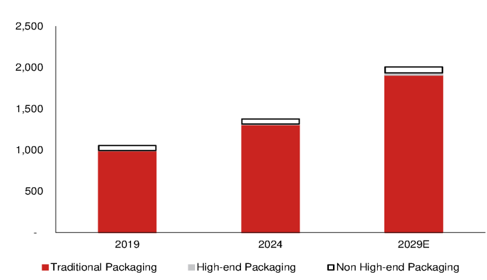
Source: Yole, Nomura research
Fig. 24: High-end advanced packaging units recorded a 31% CAGR over 2024-2029E
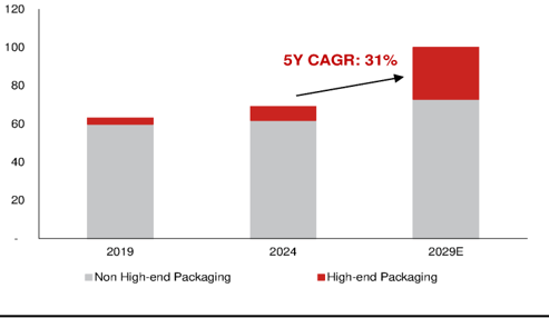
Source: Yole, Nomura research
M wafers, 300mm Eq.
160
140
120|
100
60|
40|
interconnects. Micro and Nanotechnologies/Microelectronics.
100um
20um
(M wafers, 300mm eq.)
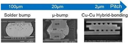
Fig. 25: Bump pitch is shrinking
ПІШІ
2018
2019
02634259
Source: TechInsights, Nomura research
Iivuule yelu will oly mically plunge witlout ules will yoon chloug" yielu
Multichip Module Yield vs. Single Die Yield
TDP (W)
100%
7,500
90%
80%
70%
6,000
70%
4,500
2um Pitch
60%
50%
40%
60%
Source: Imed Jani, Nomura research
Source: Imed Jani, Nomura research
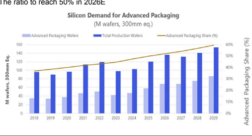
Fig. 27: Advanced packaging share of total silicon is increasing rapidly
The ratio to reach 50% in 2026E
Source: TechInsights, Nomura research
50%
3,000
40%
30%
20%
1,500
10%
0%
0
Advanced Packaging Share (%)
99% Die Yield
Fig. 26: TDP of nVidia products
Ampere
A FAIL
6kW?
Source: Company data, Nomura estimates
Fig. 28: Advanced packaging drives importance of KGD
Module yield will significantly plunge without dies with good enough yield
Source: Delphon Industries, Nomura research
Testing process changes along with chip complexity
We briefly introduced the semiconductor testing process in our Dec 2024 report (see KYEC initiation ). Typical semiconductor testing could be divided into chip probing (wafer sort/CP) and final testing (FT), and FT could include/be extended to burn-in test (BIT)/system-level -test (SLT). Along with higher chip complexity, and thus higher chip contents from advanced technologies, some changes have emerged in testing flows:
Growing trend of testing flow: additional test insertions and trend of shifting left
New technologies such as CPO will create brand-new testing insertions (see Silicon photonics to lead the next frontier ), which are totally different from the traditional testing process, creating more opportunities for the testing supply chain. Apart from CPO, many new technologies are under development such as panel-level-packaging (PLP), SoIC/3D stacking, glass core substrate (see Fig. 32 ; we mentioned some technologies in our Apr and June Anchor reports). New packaging methods will require new testing techniques (equipment, consumables, and processes). As many of these methods are still under development, we would only have clarity on the testing process when mass production approaches.
As for the existing testing flow, in the monolithic die era, assembly defects and functionality at speed are tested at package level, and functional requirements for these packages parts are similar to those at the die level. Migrating to the heterogeneous package era, when dies in different process nodes or even from different manufacturers (e.g. HBM) are put together in one package, more comprehensive testing for individual dies is necessary. Some assembly defects after the package of a particular die is hard to detect, and functionality of each single die could be different from the packaged level IC.
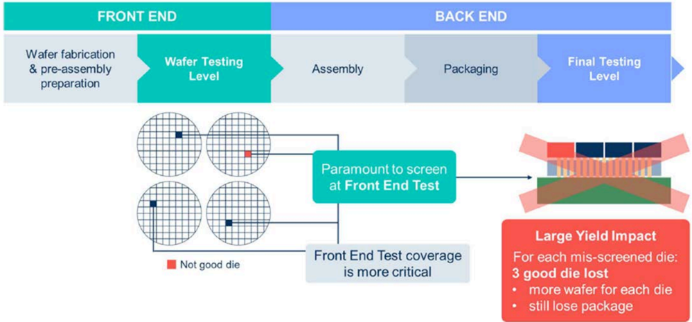
As shown in the yield cliff effect (Fig. 28 ), all of these result in an emerging trend of
Te tollu Ul ormully loll
BACK END
Front End Test coverage
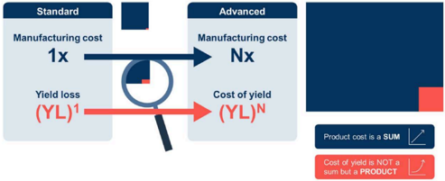
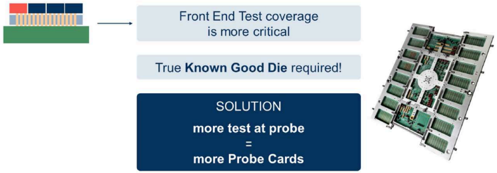
'shifting left', namely the front-end testing process is increasingly critical: one die defect in a package will create waste of other good dies, and the cost of yield increases exponentially. More front-end testing demand is leading to higher demand for probe cards (Fig. 29 - Fig. 31 ). However, increasing the focus on wafer probing does not necessarily mean it would be at the expense of final test , as single ICs function, speed, tolerance, electronic consumption, electronic emission and heat diffusion, etc, are also crucial to be reviewed at the package level, as well as seamlessly integration between different dies. The die-to-die interconnect within a package also requires additional testing efforts. The assessment metric, Defective Parts Per Million (DPPM), would be reviewed in both individual die level and packaged IC level.
Fig. 29: Frond-end test becomes more critical in the chiplet era
The trend of shifting left
Final Testing
Level
Large Yield Impact
For each mis-screened die:
Front End Test coverage
Fig. 31: Shifting left drives more probe card demand
Source: Technoprobe, Nomura research
Fig. 30: Cost of yield increases exponentially in the APT era
Source: Technoprobe, Nomura research
Source: Technoprobe, Nomura research
Fig. 32: Packaging technology trends
Advanced packaging will drive innovations in testing as well
| Technologies | Current | Future |
|---|---|---|
| Chiplet and HI | • Chiplet in PC/ server processor • HI in SiP, memory, processor, sensor, etc. | • Chiplet in mobile, consumer, automotive & other industry • More HI adoption in all market |
| 2.5D Interposer | • Si Interposer • Organic Interposer (with RDL and bridge) | • More organic interposer; glass interposer • Photonic IC (PIC) interposer • Larger interposer to integrate more chips |
| 2.5D Bridge | • Interconnect with C2/C4 or FO-RDL • Bridge with and without TSV | • Interconnect with Hybrid bond • More bridge with TSV |
| PLP | • Used for low-end FO/FI or high-density FO • More for small package size (<15mmx15mm) | • Adopt for 2.5D interposer • For large package size (> 50mm x 50mm) • Other packaging application, e.g., power module |
| 3.0D Stacking | • W2W - Memory stacking, CIS • D2W -memory/IO + logic, face to back | • W2W- memory + logic • D2W - logic on logic, face to back and face to face |
| CPO | • OE and ASIC on different substrate • PIC and EIC side-by-side | • OE and ASIC on same substrate • Stack PIC and EIC |
| IC Substrate | • Organic Core Substrate • Substrate size ≤ 120mm x 120mm | • Glass Core Substrate • Substrate size >120mmx120mm |
Source: Yole, Nomura research
SoIC also drives test complexity, along with thermal management
We believe the development of SoIC at TSMC is worth tracking and the die stacking is driving test complexity because it buries critical die-to-die interconnects deep within silicons, which are physically inaccessible to traditional test probes. Testing must therefore shift to a more rigorous, pre-bonding wafer-level test (i.e., 'shifting left') to guarantee known good dies, since any single defective layer will ruin an entire costly multi-chip stack. Furthermore, stacking inevitably creates extreme thermal-density bottlenecks and structural stresses, forcing test systems to implement complex and possibly dual-sided probing as well as real-time thermal monitoring to identify detects.
TSMC is committed to further shrinking bond pitches for logic devices, and is currently targeting N2-on-N2 with a 6um bond pitch to be in production in 2028E, and A14-on-A14 with a 4.5um bond pitch to be in production by 2029E. TSMC has been producing N7-onN7 with a 9um bond pitch since 2023, and stacking with a 6um bond pitch has also been in volume production since 2025. The vertical logic stacking of SoIC theoretically could augment transistor counts per package, an outright indicator of computing power, without extra footprints (vs CoWoS/2.5D packaging that expands horizontally to accommodate more chips).
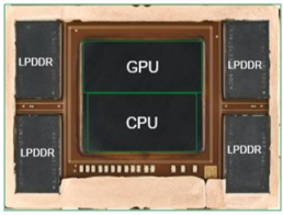
We foresee further elevating thermal challenges moving to Feynman (F100), slated for 2028E. nVidia at the GPU Technology Conference (GTC) unveiled tplans to adopt 3D stacking starting from the Feynman platform (report ). Currently, AMD (AMD US, Not rated) leads the adoption of SoIC at TSMC (starting from MI300-series), and in the latest MI450, we believe AMD stacks four top dies (four XCD) on two reticle-sized active interposers (I/O dies), in which each top die scales to about 1/3 reticle size (Fig. 92 ). Our channel checks suggest nVidia will be more aggressive in chip specs by stacking a reticle-sized GPU die on top of another for the Feynman platform, the first-ever GPU-onGPU SoIC stacking, which would lead to higher computational power even with limited growth in interposer reticle stitching size (c.6x reticle, see footprint in Fig. 93 ; up from c.5x in Rubin). Such a practice theoretically exacerbates thermal dissipation challenges.
We note there are also variants of SoIC for a broadening application base. As discussed in our 'Global Advanced Packaging - The evolution of CoWoS, SoIC and InFO ' report, our supply chain checks suggested Apple (AAPL US, Not rated) has been likely working on a few hybrid bonding/SoIC projects for M-series silicon. Apple debuted M5 Pro and M5 Max in March 2026 (press ), and we witness that Apple disaggregates CPU and GPU blocks in the previous monolithic die into discrete sub-dies, and TSMC uses SoIC-MH to bond CPU and GPU chiplets onto a passive interposer using bump-less face-to-face hybrid bonding (Fig. 39 ). While the SoIC-MH architecture is somewhat similar to 2.5D CoW, the M5 Pro/M5 Max can achieve substantially higher die-to-die interconnect density by replacing micro-bumps (2.5D CoW) with bump-less hybrid bonding, and reduce the parasitic losses (or 'chiplet tax') in chiplet-based layout.
Apart from logic-on-logic stacking, TSMC's COUPE could also serve as a key capacity
UHD FO
Molded die
Thin film RDL
IC substrate
InFO_(x)
CoWoS-R
SPIL:
• FO-MCM|
Amkor:
SWIFT
YOLE
Chan. Taraduna !
Multi-Chip
Module
(MCM)
1980
Intol:
Cannh to
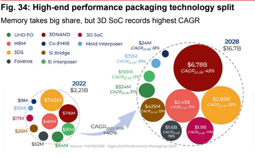
Fig. 33: High-end performance packaging types overview
lenabies mediananaling compatible with wafer)
TERADYNE
High End Performance Packaging 2023 | Report| wwwvolearoup.com |02023
Source: Yole, Nomura research
Fig. 35: Evolution of packaging method
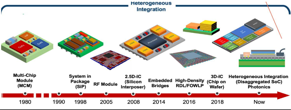
Source: ASEH, Nomura research
Fig. 36: Interposer on Substrate packaging technologies From CoWoS to CoPoS
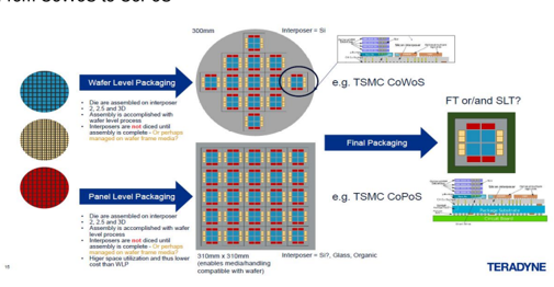
Source: Teradyne, Nomura research
InFO-LSI
VUr Vo
2.5D
3D
Melluly lanes big share, vul
ruture lestly misertons lemall to be seel!
UHD FO
• 3DNAND
Heterogeneous
• HBMI
3DS
sue leburus mynest unon
3D SoC
Advanced packaging is driving ATE TAM
Mold Interposer
$24M
CAR 22 28 18%
changes/growth with new insertions
$72M
CAR 22-28: 45%
$6.78B
Al Accelerator
$16.7B
Al Accelerator
CoWoS Package
CoWoP Package
S2.43B
CAGRI 20 599
$425M
CAR 2-30 37%
$16B
$2.85B
CAR 2-20: 25%
Integration driver of SoIC, in our view, and the company is exploring DRAM-on-logic for high bandwidth and low latency for future AI inference decoding applications. TSMC has laid out the plan to grow SoIC capacity at a >90% CAGR over 2022-27E (report ). Our current assumption is that TSMC could install >40kwpm of SoIC capacity by end-2028F, from 5kwpm by end-2025. (3D Fabric) Intel: overad CAR 22-26 3996 $1OM, $716M e.g. TSMC CoPoS
TSMC
Die are assembled on interposer
Cowos-s
Samsung, SK
YMTC
$17M.
$481M
Insertions
$26M
Source: Yole. Nomura research
Embedded High-Density (Chip on
Source: Yole, Nomura research
• Co-EMIB
Hunix 8. Micror
Samsung.
X-Cuba
Source: Teradyne, Nomura research
Find failures before packaging to reduce scrap costs and maximize package yield
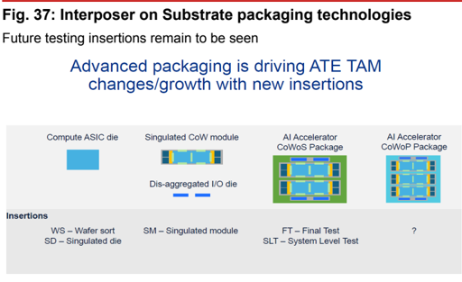
Fig. 38: Additional testing required in AI era
New Insertion
LPDDR
Wafer
Fabrication
LPDDR
Mission
Model
Probe?
Source: TechSearch International
HBM Wafer Sort smaller chips
Source: Teradyne, Nomura research
Fig. 39: A cross section of SoIC-MH in Apple M5 Pro and M5 Max
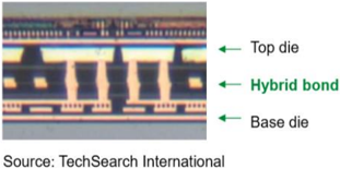
Source: Besi, TechSearch International, Nomura research
Testing equipment and consumables are clear beneficiaries under the big theme of advanced testing
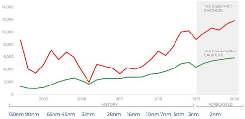
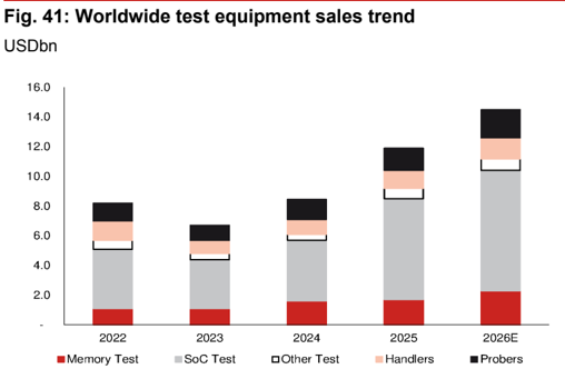
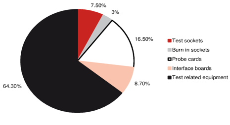
We have been turning increasingly positive on the overall back-end supply chain since 4Q25. Previously, we mainly focused on OSAT vendors, given its high correlation with front-end manufacturing. However, we now expand our coverage to testing equipment and consumables. Yole estimates that the cost of testing high-end performance packages (equipment and consumables) could be between 10% and 15% of current total test costs, and the institution also forecasts that overall test equipment and test consumables to witness a 5%+ CAGR over 2025-30E, reaching USD23bn in 2030E . TechInsights also projects test hardware spending to exceed USD20bn-plus in 2029E, from slightly higher than USD15bn in 2025E, at a 10% CAGR (Fig. 40 ).
Coupled with rising BOM share, we believe testing equipment and consumables could be
rich langes die malcalive, bourudhes betweell dujacent lechnologies die tanston cones whele solutions ovellap
• Probe Cards m Interface Boards m Test & BI Sockets
Cantilever (peripheral pad)
CACR 6.2%
Tulal mainet levellue was Uou lo.tU4044
16.0
14.0
Test Equipment a market with considerable upside potential. Other than the overall TAM increase and new testing opportunities from innovative testing methods, we have witnessed market share gains for key Taiwan suppliers, either because: 1) their key customers gain share in the AI chip space; or 2) they gain share from overseas vendors. See Taiwanese players are gaining traction in the sector for details.
25000
14,000|
12,000
20000
10,000
8,000
15000
6,000|
10000
4,000|
2,000|
Thus, we initiate coverage on key testing interface vendors WinWay and MPI, as well as initiate/resume leading testing equipment vendors Hon Precision and Chroma . We expect these companies' top line and bottom line to both outgrow the market's, mainly driven by share gains. We also reiterate Buy on ASE and KYEC . SoC Test
5000
Couran. Volo
Namura raccornh
Fig. 40: Test hardware spending trend
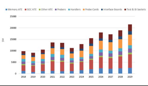
Source: TechInsights, Nomura research
Fig. 42: Both test equipment and test consumables to record a 6%+ CAGR over 2023-28E
Source: Yole, Nomura research
16.50%
+
800
8.70%
pogo pin
2024
•Other Test
•Test sockets
Burn in sockets
•Probe cards
Interface boards
•Test related equipment pitch (um)
2025
2026E
Handlers
• Probers
Source: TechInsights, Nomura research
Fig. 43: Cost of test equipment and consumables
Total market revenue was USD15.4bn in 2024
Source: Yole, Nomura research
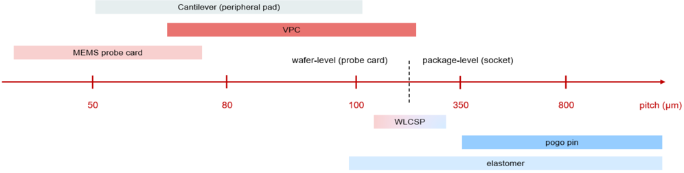
Fig. 44: Typical pitch regimes and corresponding test interface solutions
Pitch ranges are indicative; boundaries between adjacent technologies are transition zones where solutions overlap
Note: This is a conceptual illustration, not specific to any company or project.
Source: Nomura research
7.50%
3%
Teol naruware ale olippeu velore Cap maso produchion engineering / qualification
production
Fig. 45: Timeline of testing equipment and interface preparation
-12m
Test hardware are shipped before chip mass production
Test interface shipment
+
+9m
Note: This is a conceptual illustration, not specific to any company or project. Source: Nomura research
+3m
+6m
+12m
share
900000
800000
700000|
600000
500000
400000|
300000
200000
100000
EDIB
—Total DIB — Total TCS
17%
How big is the test consumable market?
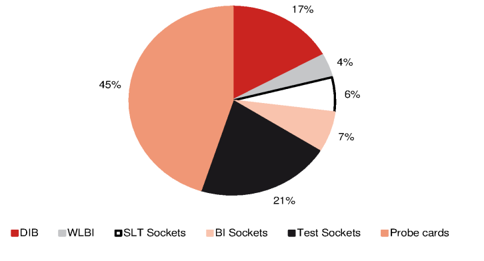
Test interface, or test connectivity/test consumables, are components used during test processes, between testers and devices under test (DUT), and these components enable electrical connections/signal transmission between devices and equipment. TechInsights estimates the test connectivity market reached over USD5.5bn in 2025, and it will reach USD8bn by 2028E (Fig. 46 ). Probe cards, sockets and device interface boards (DIB) are the three major categories, with probe cards accounting for 40%+ of the market in 2023-25. Test sockets exceeded DIB to become the second-largest segment in 2024, recording 21% of the test connectivity market, and in 2025, wafer-level-burn-in (WLBI) and BI sockets gained share (Fig. 48 - Fig. 49 ). That said, both market researches from Yole and TechInsights suggest probe cards would record the highest revenue CAGR over 2025-30E (Fig. 47 ) - underscoring the views of putting more focus on wafer sort and that competition in the probe card segment will intensify.
Fig. 46: Semiconductor sales vs. test connectivity sales
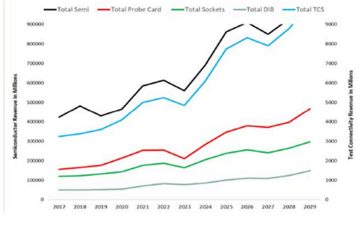
Note: TCS: Test Connectivity System
Source: TechInsights, Nomura research
Fig. 48: Test connectivity market - 2025
Probe card maintains the largest segment while burn-in socket is gaining share
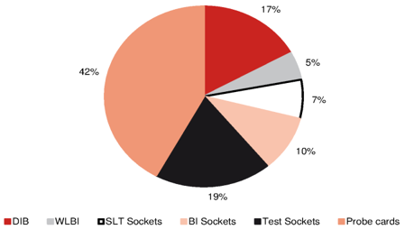
Source: TechInsights, Nomura research
2030
21%
•Test Sockets
•Probe cards
Fig. 47: Test connectivity - relative 5-year growth trends
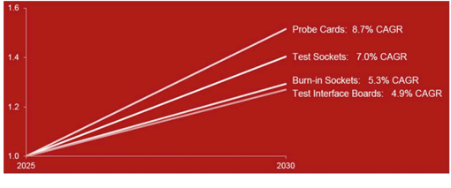
Source: Yole, Nomura research
Fig. 49: Test connectivity market - 2024
Test socket exceeded DIB in 2024
Source: TechInsights, Nomura research
9000
1.6
Probe Cards: 8.7% CAGR
17%
Test Sockets: 7.0% CAGR
4%
Burn-in Sockets: 5.3% CAGR
Test Interface Boards: 4.9% CAGR
6%
7%
Probe card accounts for 40%+ of the test connectivity market
Probe card market to grow from ~USD2.8bn in 2025 to USD4.5bn+ in 2030E
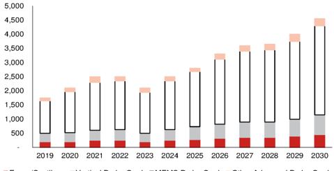
According to TechInsights' statistics, total semiconductor probe card market sales recorded ~USD2.8bn in 2025. Within the probe card market, nearly USD2bn was MEMS probe cards, accounting for around 70%. TechInsights projects that the probe card market will exceed USD4.5bn in 2030E, recording a 11.1% CAGR over 2025-30E ( Fig. 50 ).
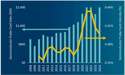
FormFactor, a leading probe card vendor, compared semi probe card sales with total semi sales, and concludes that over the past 16 years, investment in probe cards has tripled, and test intensity is increasing to avoid chip failures. The trend is fueled by increased adoption of advanced packaging. The intensity increased 10% to ~0.4% in 2024 (Fig. 51 ).
Two global players leads the sector - Technoprobe and FormFactor; MPI follows in non-memory sector
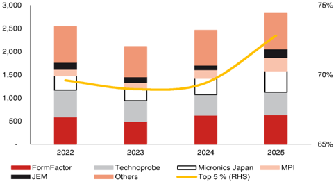
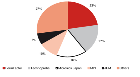
There are two leading probe card vendors globally - Technoprobe (TPRO IM, Not rated) and FormFactor (FORM US, Not rated). Yole's statistics show that FormFactor leads in total own make IC probe card vendors, but if excluding memory probe cards, Technoprobe would take the lead. Based on 2025 probe card revenue, FormFactor recorded USD638 mn, taking a 23% share of the probe card market, and Technoprobe stood at the second place with a ~17% share. The top 5 vendors took a combined 73% share in 2025 (Fig. 52 - Fig. 53 )
FormFactor excels in both logic and memory: A key memory supplier accounted for ~30% of its total revenue in 1Q26, and nVidia surpassed 10% for the first time in the same quarter thanks to networking applications. Besides, Intel (INTC US, Not rated), Samsung (005930 KS, Buy), and TSMC are also its top customers. Compared to Taiwan peers, FormFactor has more standard products (e.g.memory) and could be less willing to offer customization. However, the company has begun to ramp test system for CPO Insertion 1 and raised CPO revenue guidance during its April earnings call, and CPO is a segment we believe has significant growth potential for the testing supply chain (as mentioned in Silicon photonics to lead the next frontier ).
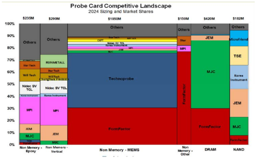
Technoprobe dominates in MEMS: Technoprobe has in-house MEMS fab utilizing semiconductor lithographic precision technologies, and its expertise in MEMS technology supported its share gain from ~8% in 2018 to ~16.5% in 2025, according to Dataintelo Analysis; specifically, it took 60% of the MEMS logic probe card market in 2024 (USD937mn market size). It sells not only turnkey probe cards, but also sell probes externally.
Micronics Japan (MJC) and Japan Electronic Materials (JEM) specialize in memory probe cards: these two Japanese players have niche in the memory probe card segment. MJC (6871 JP, Rating suspended) concentrates on the high-end memory/HBM segment which has a larger revenue scale, while JEM (6855 JP, Not rated) slightly lacks behind MJC and FormFactor, but it has higher exposure to NAND.
MPI aggressively catches up in the MEMS market: MPI leads in cantilever and vertical probe cards in terms of market share (Fig. 56 ), but the company is also proactively expanding MEMS capacity to catch up with testing requirements for AI chips, and to compete with top suppliers.
We see more Taiwanese players targeting the probe card market
Given that probe card is the largest segment in the test connectivity market, and with the market expecting the probe card market to outgrow other segments despite having a large base (per abovementioned reasons and trends), we see more activities in the field.
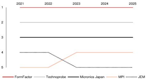
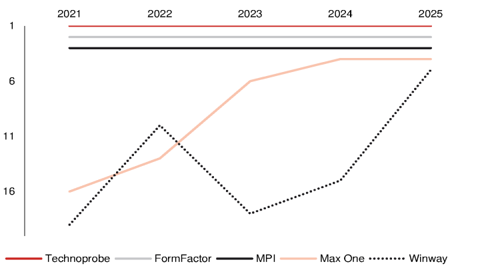
We see MPI gradually take share in the self-made IC probe card market, from No.5 in 2021 to No.4 since 2023 (surpassed JEM in 2023, Fig. 54 ). MPI's revenue share in the probe card market grew from ~6% in 2023 to ~10% in 2025 (Fig. 53 ). Excluding memory probe cards, MPI has maintained its position at No.3 (Fig. 55 ), after Technoprobe and Form Factor. WinWay and CHP T (6510 TT, Rating suspended) are also good examples, both of which have their own expertise with decent market position (socket and PCB), but they are actively pursuing opportunities to make inroads in the probe card market. WinWay's progress is ahead of CHPT with its probe card vendor (non-memory) ranking jumping from No.19 in 2021 to No.5 in 2025 (Fig. 55 ), mainly on strong demand from gaming graphics. See Taiwanese players are gaining traction in the sector sections for details between these Taiwanese suppliers and their offerings.
vil to grauually yammy orate
Millio cuntues lo be major type, roughy ror
Deople stable lalkly, Mrl ls giduually gamily share
3,000
5,000
4,500
2,500
4,000
2
3,500
2,000
3,000
2,500
1,500
3
2,000
1,500
1,000
4
1,000
500
500
5
2024
Fig. 50: Global probe card revenue
MEMS continues to be major type, roughly 70%
2019
• FormFactor
JEM
FormFactor
Source: TechInsight, Nomura research
75%
70%
Source: TechInsight, Nomura research
Fig. 52: Total probe card market by vendor
Despite stable ranking, MPI is gradually gaining share
Source: Company data, Nomura research
Fig. 54: Global own make IC probe cards venders ranking MPI is gradually gaining share
Source: Company data, Nomura research
2025
ramallooe playolo manly duurcos not temuly marnel rup o playels account lor 07o or the markel
2021
2022
Semiconductor Probe Card Sales (SM)
•FormFactor
2024
23%
27%
Fig. 51: Investments in probe is increasing in recent years
0.41%
- Technoprobe
Source: FormFactor, Nomura research
Fig. 53: Market share split of 2025 total probe card market
Top 5 players account for ~70% of the market
Source: Company data, Nomura research
Fig. 55: Global non-memory probe cards venders ranking
Taiwanese players mainly address non-memory market
Source: Company data, Nomura research
$2,400
2023
1
11
2025
franut un ablut leaus not memory Memo mainel
$235M
$290M
$1050M
Others
$150M
Others
$420M
Others
$182M
Others
Fig. 56: Probe card competitive landscape in 2024
TPI and FormFactor leads non-memory MEMS market
Star Tech
Will Tech
Nicec SV
TCL
MPI
JEM
MJC
Non Memory -
TSE
Epoxy
Source: TechInsights, Nomura research
4%
12%
Fig. 57: Global probe card market by revenue from vendors' headquarters (2025)
Europe
•Japan
South Korea
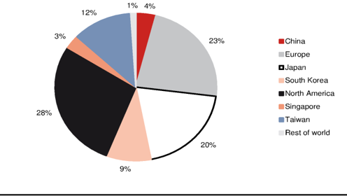
28%
Source: TechInsiahts. Nomura research
Source: TechInsights, Nomura research
Socket market size relatively stable with shifting market share
Total test socket market revenue to witness mid-single-digit CAGR over 2025-30E
Sales of combined test sockets (including packaging testing, SLT and engineering testing) and burn-in sockets were estimated at ~USD1.9-2bn in 2025E (~36% of the test connectivity market), and are projected to reach USD2.4bn in 2030E, at a ~5% CAGR over 2025-30E, according to TechInsights. Test sockets account for ~70% of total socket market, and burn-in sockets the remaining ~30%. Similar to the market for other testing hardware, that for sockets is also growing in tandem with advanced packaging units (Fig. 23 - Fig. 24 ), and TechInsights forecasts BI socket revenue to slightly outgrow the test socket market's revenue over 2025-2030E, at 5% and 4% CAGRs, respectively ( Fig. 58 ). However, Yole's projection suggests test sockets could outgrow BI sockets over 2025-30E, at 7% and 5.3% CAGRs, respectively ( Fig. 61 ) , citing reasons such as increased use of SLT and WLBI (WLBI uses specialized probe cards), and relatively stable burn-in testing time.
Test socket usage increases rapidly with longer testing times, larger package sizes, complicated package methods and increased test insertions (for example, additional insertions for CPO). On the other hand, we expect more AI chips to adopt the burn-in process, penetrating gradually from nVidia GPUs to key ASICs such as TPUs/CPUs, and conducting burn-in could potentially increase FT processes as well (FT1 and FT2, before and after burn-in). We believe different vendors have their own considerations on testing processes, also depending on end application and user scenarios, but we expect an increase in testing intensity overall. We therefore like the overall testing sector, spanning from OSATs and equipment vendors, to consumables suppliers.
Different vendors specialize in different types of sockets
There are many socket players in the world, focusing on separate fields, with no single player dominating the market (top players each only take a 5-15% share in the test socket market, and each take a 10-20% share in the burn-in market) ; thus, the gaps between players are also relatively small, especially after the AI/HPC boom - the ones that win key projects will show significant revenue expansion with market share gains in the periods of test interface shipment (usually before chip mass production), in our view.
Key players in the field include:
Yamaichi (6941 TT, Not rated): a leading Japanese vendor in both test and burn-in socket markets with diversified end-application exposure, spanning from auto to smartphones. Yamaichi specializes in fine-pitch pogo pin test and burn-in sockets, and has close relationships with IDMs/automakers. It also engages the AI/HPC sector through HBM (primarily Samsung). Other notable customers include TSMC and Apple. Yamaichi and Enplas both have expertise in precision engineering.
LEENO (058470 KS, Buy): LEENO is a vertically integrated socket player based in South Korea, mainly in test sockets field with less burn-in exposure. 100% in-house manufacturing drives its industry-leading profitability and supports the shortest lead time, in our view. LEENO provides solutions to both memory and logic product makers; its flagship smartphone AP is one of its key revenue growth drivers (e.g., from Apple, Samsung, MediaTek and Qualcomm [QCOM US, Not rated]).
FEINMETALL
100%
90%
80%
70%
60%
50%
40%
30%
20%
10%
0%
1%
Enplas (6961 JP, Not rated): another Japanese socket vendor, but highly skewed to burn-in sockets with proprietary micro fabrication technology. Other than GPUs, Enplas has been expanding its exposure to AI ASICs and they set SLT market as a growing area to address, besides burn-in. Automotive SoCs are also one key driver of its semiconductor business.
Yokowo (6800 JP, Not rated): Yokowo specializes in micro precision processing technology, offering a broad range of contact probes and circuit testing connectors. It provides sockets itself, but it also sells pins to external vendors such as WinWay. In addition, Yokowo also provides pogo pins to probe card vendors for RF applications due to high-current features. Well-known customers include Intel and Qualcomm.
ISC (095340 KS, Not rated): ISC is aggressively pushing its proprietary elastomer-based conductive silicone rubber technology, with one notable partner Samsung. Following SKC's (a subsidiary of SK Group) acquisition of ISC in 2023, the latter (ISC) has become more structurally aligned with the memory sector.
Smiths/IDI (SMIN LN, Not rated): Smiths Group purchased IDI (Interconnect Devices) in 2010 and transformed it to Smiths Interconnect. In 2025, the Smiths Interconnect division was sold to Molex. The company is well known for its DaVinci series coaxial sockets, focusing on high-frequency connectivity. The company are key suppliers to key GPU and ASIC vendors.
WinWay: WinWay mainly focuses on logic space test sockets, and its close relationship with top key fabless vendors has led the company to rapidly gain share in the market, along with the AI/HPC/advanced packaging trend. The company has expertise in highdensity coaxial sockets, and it has further enhanced its proprietary product, HyperSocket, to capture further testing challenges.
Cohu (COHU US, Not rated): Cohu has broad product portfolio covering ATEs, handlers, sockets, burn-in boards, and thermal solutions. Due to its heavy exposure to more legacy products (auto, industrial, RF), its market share in sockets has gradually faded.
AI/HPC set the stage for high-performance socket players such as WinWay
Compared to the probe card market, the socket market is relatively dynamic, as shown in Yole's peer ranking over the past several years, with a reshuffle almost every year (Fig. 62 - Fig. 64 ). In our view, two factors impacted the competitive landscape: the consumer/mobile downturn in 2023, and the AI/HPC boom that followed which rewarded vendors positioned in high-performance test sockets.
The top vendor has alternated between Yamaichi and LEENO: The likely explanation lies in their different end-market exposures. The 2023 downturn hit memory, smartphones, and consumer semiconductors hard (segments in which Yamaichi has deep roots), while LEENO's strong position in probe pins and sockets tied to the Korean memory ecosystem let it hold up relatively better and claim the 2023 crown. As memory (particularly HBM for AI) rebounded strongly in 2024-25, LEENO regained momentum and retook the first place in the preliminary 2025 ranking.
Yokowo's and Cohu's disappearances: Fourth overall in 2022, Yokowo fell out of the top five entirely from 2023 onwards, which is consistent with heavy exposure to smartphone and consumer applications that never recovered to pre-2023 levels (Fig. 62 ). Cohu climbed from third to second in 2023 but then fell back to the third place in 2024 and fifth in 2025 (Fig. 63 ) - a pattern consistent with its broader exposure to automotive and industrial test, both of which did not see strong demand recovery in 2024-25 while AI boomed.
The AI-driven winners: WinWay and Smiths Interconnect are widely associated with high-performance test sockets for AI accelerators and HPC devices, where socket content per device (larger packages, more pins, higher power and bandwidth requirements) is far more valuable than in consumer parts. We observe the two companies ranking gradually rose in past several years (Fig. 63 ).
Compared with the test-socket market, burn-in sockets look remarkably calm: The same large names appear nearly every year as market share leaders, with only the order changing (Fig. 64 ). As mentioned above, more and more AI chip companies have adopted the burn-in process, but different technology focuses in burn-in (qualification cycles, reliability requirements, long-standing customer relationships) have kept the same players entrenched, while the test socket segment is where share seems to us to be genuinely up for grabs, because AI design wins can transform a vendor's revenue in a
vvlmle tlaumtluhal sucnel Walnel may olaulloe Ul evell ueulllle
Ranking changes every year in total socket market
2,500
1,250
2
1,000
2,000
3
4
1,500
750
1,000
single year.
Fig. 58: Global test and burn in socket revenue
Total socket revenue to reach USD2.4bn in 2030E
500
Yamaichi
Melluly mainel las vu grown non memory deople omallel portion
1.6
2,500
2024
2,000
1.4 -
1,500
12 -
1,000
LEENO
— Enplas
Yokowo
- Winway
500
250
2019
2016
- LEENO
***.-- Cohu
...
Cohu
Winway
•.•.•.... ISC
Advantest
500
2025
Source: Yole, Nomura research
Burn in socket suppliers are relatively stable
1
2
3
2023
2024
Probe Cards: 8.7% CAGR
Test Sockets: 7.0% CAGR
Burn-in Sockets: 5.3% CAGR
Fig. 59: Global socket market by application
Memory market has outgrown non-memory despite smaller portion
......... Smiths Interconnect
• Yamaichi
-
Enplas
-
Okins
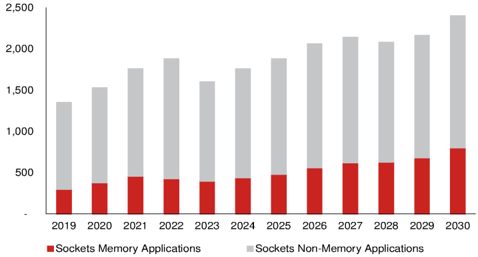
Source: TechInsights, Nomura research
Fig. 61: Yole projects higher revenue growth for test sockets vs. burn-in sockets
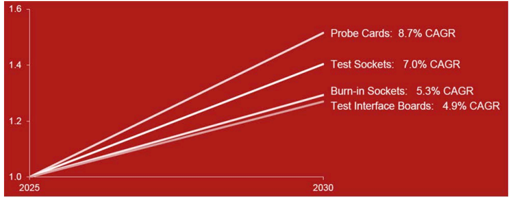
Source: Yole, Nomura research
Fig. 63: Global test socket market ranking WinWay and LEENO took the lead in the past two years
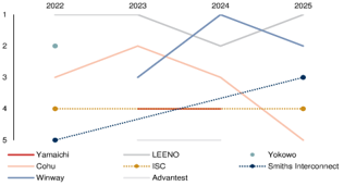
Note: *2025 ranking is preliminary.
Source: Yole, Nomura research
Fig. 64: Global burn in socket market ranking
Burn in socket suppliers are relatively stable
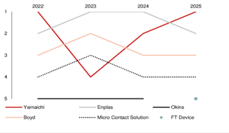
Note: *2025 ranking is preliminary.
Source: Yole, Nomura research
2022
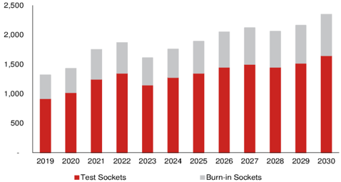
Source: TechInsights, Nomura research
Fig. 60: High-performance socket market to grow at 9% over 2025-30E
While traditional socket market may stablise or even decline
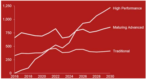
Source: Yole, Nomura research
Fig. 62: Global test and burn in socket market ranking
Ranking changes every year in total socket market
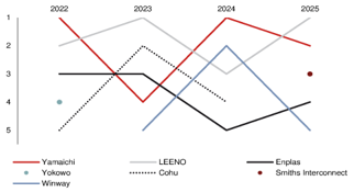
Note: *2025 ranking is preliminary.
Source: Yole, Nomura research
2025
.........•
2025
2022
2023
High Performance
• Smiths Interconnect yealo
Cooperation between testing industry players
An interesting point within the testing sector is the close relationships between companies. We see a wave of consolidation (Fig. 65 ) and strategic alliances, possibly driven by the need to tightly integrate ATE with test sockets and probe cards to address the complexities of advanced packaging (like chiplets and CoWoS), HBM, and silicon photonics. We also see substantial outsourcing activities between the players, likely due to the supply-constrained environment, even though turnkey/total solutions still produce higher margins/ASPs.
External procurement of probes increasingly common
In Aug 2025, WinWay and Yokowo announced an MOU on a strategic alliance. Based on our understanding, WinWay outsources a part of its socket pogo pin from Yokowo. In Oct 2025, CHPT and Yokowo signed an investment deal in which CHPT will invest USD2mn in Yokowo via subsidiary TestPro (unlisted), and Yokowo will invest USD2mn in CHPT. The cooperation between CHPT and Yokowo could be traced back to 2018, as CHPT wanted to focus on MEMS pins, but still needed pogo pins to test large pitch wafers for RFFE, power devices and/or sensors. Yokowo is one of the most vertically integrated probe manufacturers - it runs large fleets of probe-making lathes with fully automated assembly and inspection lines, plus in-house moulding and plating. Through external procurement from Yokowo, the two players can either relieve capacity shortage, or spend more time on focus areas. On the other hand, Yokowo can broader its customer base and penetrate into the AI/HPC market through the two key players.
In Dec 2025, Technoprobe and WinWay signed an agreement for TPI to act as a developer and manufacturer of testing solutions, granting WinWay the right of use for fiveyear period. Via the agreement, WinWay secures necessary probes to support its business ambition in the MEMS probe card market targeting the most advanced AI chips.
ATE vendors divest test interface divisions for hyper-specialisation while making equity investments to strengthen collaboration toward advanced packaging
We observe some industry dynamics in the test hardware markets, between ATE and probe card vendors. In 2020, FormFactor acquired probe card assets from Advantest (6857 JP, Buy) to increase exposure in the NAND Flash market. In Nov 2023, Teradyne (TER US, Not rated) and Technoprobe announced a strategic partnership in which Teradyne invested USD516mn in TPI, and TPI acquired TER's Device Interface Solutions (DIS) business for USD85mn, only several months after they acquired TIB maker Harbor Electronics (unlisted) in Aug 2023.
Advantest is also aggressive, after assembling Advantest Interconnect (AIS) through serial acquisitions (Essai sockets, R&D Altanova boards, Shin Puu test-board PCB), it invested in early 2025 in both Technoprobe and FormFactor , with technology and PCB manufacturing partnerships. In our view, these activities imply two converging forces: hyper-specialization and consolidation. ATE manufacturers are increasingly shedding peripheral hardware divisions to focus exclusively on their core competency, i.e. complex system architecture and software. On the other hand, interface providers concentrate purely on micro-mechanical and metallurgical innovations. Simultaneously, this extreme division of labor has triggered a wave of strategic M&A and cross-investments among key players. By joining forces, we believe these market leaders are aiming to ensure that highly specialized test instruments and interface hardware are co-engineered seamlessly to deliver turnkey, high-yield solutions for the next generation of silicon.
The ecosystem co-engineering trend is particularly pronounced in the era of advanced packaging and when complex testing processes are required. Given higher and higher costs of failure, all players within the testing supply chain are activity forming crossboarder cooperation. One example is FormFactor's TRITON system (a comprehensive test-cell), developed by FormFactor (interface/prober), Advantest (ATE), and Tokyo Electron (8035 JP, Buy; prober) to address single-sided wafer testing (Insertion 1, in our view, see Silicon photonics to lead the next frontier ). In the AI test era, co-design value across tester, boards, and probes has risen sharply, elevating interface hardware from consumables to a strategic layer to be owned or bound.
Fig. 65: Major M&As in testing sector
Cancadel Axext!
Advantest acquires essai
Teradyne acquires Lemsys
ADVANTEST
2016
Advantest acquires
R&D Altanova
ADVANTEST
Zero One acquires advanced PCB
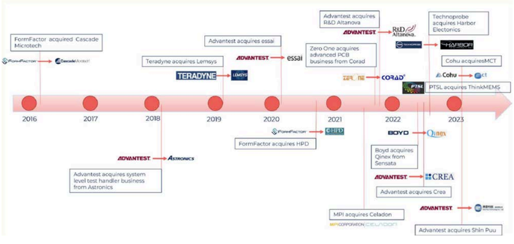
Source: TestConX, Nomura research essai
REDE
Vitanova
Technoprobe acquires Harbor
Electonics
HARBOR
Cohu acquitesMCT
Taiwanese players are gaining traction in the sector
Along with this report, we initiate coverage of four companies with Buy rating s : MPI (6223 TT), WinWay (6515 TT), Hon Precision (7769 TT), and resume coverage of Chroma (2360 TT) , which has products spanning probe cards, sockets, and testing equipments, respectively. We hold an overall positive view on the testing sector and each player, as each specializes in different segments, and has own long-term partnership ecosystem and customer base. They may compete in some specific projects, but as long as AI/HPC chip demand sustains, we see the market keep enlarging and can fit many players in the field. Also, we believe Taiwanese players as a whole will gradually gain share from overseas leading players, likely due to close relationships with key fabless and spillover effect from capacity optimization, share gains of their customers, and advantage to provide on-site real-time support in the Taiwan semiconductor ecosystem.
Test interface quartet: MPI, WinWay, CHPT, and Keystone
Taiwan hosts a distinctive cluster of semiconductor test-interface suppliers that emerged around the comprehensive ecosystem (foundries/fabless/OSATs). The four companies are usually discussed together, but they occupy different positions along the test-interface stack: probe cards, load boards, sockets etc. See Fig. 66: Comparison of major Taiwanese test interface suppliers .
All four companies sell device-specific, design-to-order test interfaces: each new chip design requires a newly engineered card, board, or socket, and large volume pull in usually happens before chip production ramp-up (repeated orders are placed after mass production whenever necessary). In this framework, MPI dominates US ASIC vendors with in-house probe cards, with CPO equipment opportunities emerging. WinWay's socket business mainly ties to major US GPU suppliers and some ASIC vendors, and it has obvious progress in MEMS probe cards as well. CHPT concentrates on high-end custom boards with in-house manufacturing depth, proactively developing more turn-key opportunities. Keystone wraps its board portfolio in an on-site service model.
By scale and market cap, MPI is the largest of the four (Fig. 66 ), and relatively diversified (it derives 20-30% of sales from equipment), followed by WinWay, CHPT and Keystone. Their overlapped business is the probe card business, and we think the major differences are: MPI has a broad customer base with relatively small MEMS penetration now (we see the migration is gradually happening), and it has 100% in-house probes and substrate fabrication. WinWay's probe card business is anchored on nVidia, and it purchases MEMS probes from Technoporbe. CHPT's revenue from probe cards and load boards accounts for 60%+ of total revenue, and its relationships with key fabless are determinants of its future project wins. KSMT operates a fabless business model (it does not have fabs for probe cards and boards). It has a higher revenue proportion from load boards than probe cards, and is well-known for its R&D resources integration capabilities.
Fig. 66: Comparison of major Taiwanese test interface suppliers
| CHPT (6510 TT) | MPI (6223 TT) | WinWay (6515 TT) | KSMT (6683 TT) | ||
|---|---|---|---|---|---|
| Financials | Market cap (USDbn)* | 2.74 | 18.16 | 7.24 | 1.04 |
| 2025 Revenue (TWDmn) | 4,806 | 13,371 | 7,857 | 2,136 | |
| 2025 GM (%) | 55.5% | 55.6% | 45.3% | 46.1% | |
| 2025 OpM (%) | 24.8% | 28.2% | 26.3% | 25.2% | |
| 2025 EPS (TWD) | 30.41 | 33.49 | 46.93 | 15.42 | |
| Probe card | 65.0% | 72.2% | 29.0% | 36.5% | |
| Socket | 56.0% | ||||
| 2025 Product mix | Load board/BIB/SLT board | 25.0% | 61.6% | ||
| Contact element | 11.0% | ||||
| Equipment | 26.1% | ||||
| Others | 10.0% | 1.7% | 4.0% | 2.0% | |
| Probe card PCB | O | ∆ | ∆ | ∆ | |
| Probe card interposer/substrate | O | O | ∆ | ∆ | |
| Product coverage (mfg/design) | Probe head/probe card assembly | O | O | O | ∆ |
| - MEMS probe capability Sockets | O (in-house) | O (in-house) | O (third-party) O | O (third-party) | |
| ∆ | |||||
| Load board/BIB/SLT board Probe card PCB/Load board | O Capacity to triple in 1Q27 vs. end-25. Fab 3 to ramp in 2028. | In-house PCB fab to ramp in 2H27 | |||
| Capacity | Probe card pins | CPC: ~500kpm VPC: 1,200/2,000 kpm MEMS: 1,000/3,500 kpm in end-2025/26F | |||
| Sockets | Capacity to be more than double in 2026F vs. 2025 | ||||
| Catalysts | AI hype and new project announcements | GPU ramp; key ASIC ramp | Key ASIC ramp; CPO | GPU ramp; key ASIC ramp | project win |
| Risks | AI demand deterioration | No progress in turn-key | CPO & ASIC delay | Key projects delay; profitability headwinds | project loss |
Source: Company data, Bloomberg Finance L.P., Nomura research
Chroma vs. Hon - little overlap in business scope
A frequently asked question by investors is whether and where Chroma competes with another Taiwan-based backend testing equipment maker Hon. Precision (7769 TT, Buy). Admittedly, both the companies have ATC/handler offerings for FT and SLT, but we believe they have fairly little business overlap given Chroma's focus on SLT handlers (we estimate 60-70% of Chroma's semiconductor testing revenue comes from SLT) vs Hon's focus on FT handlers (70-80% of handler revenue comes from FT).
Hon has been making inroads into the SLT handler market by leveraging its competency in customization and ATC, and we believe AMD is one of its longstanding customers in SLT handlers, although we think Chroma could have secured SLT handlers for AMD's latest MI400-series. We are aware that Hon has started engineering collaboration with nVidia in SLT handlers for the future generation of AI GPUs, but we are uncertain about whether Hon could really challenge Chroma's dominance in this segment. In our view, Hon's new SLT handler opportunities could lie squarely within ASIC customers whose broader adoptions of SLT, apart from mandatory FT, have significantly increased.
Key test consumables and equipment within the testing process
How does test hardware work together in the testing process?
A typical testing process including chip probing (CP) during wafer stage (before dicing, before packaging or after wafer-level packaging) and final testing (after dicing), see our Dec 2024 KYEC initiation report, as well as the Testing process changes along with chip complexity section of this report for more details on testing flows.
A tester (also called Automatic Test Equipment [ATE]), usually from Advantest or Teradyne, is used in both the CP and FT stages, while it needs to work with prober/handler respectively, as well as different test interfaces:
IC test trios: ATE, prober/handler, and test interface
Semiconductor testing is not carried out by one single tool but by a tightly integrated system also known as a 'test cell'. The test cell consists of three major parts: automated test equipment (ATE), prober/handler, and application-specific test interfaces. In SLT, the ATE is replaced with a system test board on which test sockets are equipped, housed inside an SLT handler.
- Automated test equipment (ATE): ATE, or simply 'tester', is the sophisticated core workstation of the test cell that feeds precise electrical stimulus signals (e.g., voltages, currents, or high-frequency waveforms) into the device under test (DUT) and monitors the output responses. The tester compares the chip's real-time performance running on pre-programmed inputs against engineering design specifications to identify defectives. In the ATE architecture, the mainframe houses the tester's power supply, central cooling unit and the system controllers, and the test head houses the test interfaces. ·
- Prober/handler: The prober or the handler is the mechanical automation arm of the test cell that operates with the ATE to ensure a continuous, high-speed, and unmanned silicon test flows. The test head is flipped and pneumatically or hydraulically docked into the core mechanical nest of the prober/handler. The prober and the handler are used in different testing scenarios the prober is present in CP and handles uncut wafers, using microscopic pins to physically contact with individual die before they are singulated, while the handler picks up chip packages (in FT or SLT) from trays, inserts them into the test sockets, and physically sorts them into different bins based on the tester's verdict. ·
- Test interface: The test interface is the physical and electrical 'bridge', customized based on the silicon layout/package, to connect the generic tester to the DUT. A probe card paired with pogo pins (or MEMS pins for fine-pitch applications) is being used in CP, while a load board with test sockets is adopted in FT. ·
The IC test squad is not complete without 'role players'
Beside the aforementioned trios, we note there are also tools supplementing temperature management to prevent undesired shifts in chip performance and physical properties under different thermal conditions, and specialized plug-in modules to expand or reconfigure the tester's scope.
- Thermal chuck: During CP, the chuck is the flat, rigid metallic platform that holds the silicon wafer in place using vacuum suction. A thermal chuck is a chuck with built-in heating elements and internal cooling channels to uniformly control the temperature of the wafer under test when mimicking different thermal conditions in operations. A thermal chuck must demonstrate extreme planarity (i.e., very meager warpage) at extreme temperature swings to avoid poor electrical contacts or wafer crack by probe needles. ·
- Active thermal control system (ATC): ATC is a dynamic temperature management system integrated into the handler. When a tester boots up workloads, the DUT could undergo a spike in internal power density and instantaneously heat up. ATC detects the thermal conditions of the chip under test and instantly adjusts its cooling/heating action to counteract the chip's internal power fluctuations. ·
- Instruments: The tester is essentially a modular chassis populated by a cluster of instruments that define its initial testing scope. However, if a silicon requires test ·
Main board (PCB)
LSI tester
Fixing implement coverage beyond this built-in set, specialized instruments can be added to the tester to extend its capabilities. These modular instruments are notably critical for highperformance domains such as analog/mixed-signal and high-speed digital, and instruments are introduced in CPO test insertions to assist with photonic test items. Performance board
Signal path and space transformation in ATE systems
Wafer prober
The signal path within the ATE flows sequentially from the tester to the device under test (DUT). Initially, the ATE's internal instrument cards generate and measure the necessary testing signals. These signals are transmitted through thousands of double-ended spring pins (pogo pins) housed within the pogo block on the test head interface. Internally, the upward-facing ends of these pins make direct physical contact with the ATE's precision instrument cards or internal cable routing boards. Subsequently, the signals are routed and fanned out by a highly customized printed circuit board . Depending on the test phase, this is either a probe card PCB mounted on a wafer prober for Wafer Sort (CP), or a load board docked with an IC handler for Final Test (FT). For advanced CP applications, a space transformer (such as MLO or MLC) is further utilized to drastically reduce the routing pitch before reaching the final contact elements, which consist of micro-probe needles for CP or socket pins for FT. The primary objective of every structural layer is space transformation: shrinking the tester's coarse, millimeter-scale pin grid down to the microscopic die pad pitch (~40-100 µm) or package ball pitch (above 100 µm), while rigorously preserving signal integrity and power delivery efficiency.
Mechanical actuation and system communication
On the mechanical front, the heavy test head is maneuvered by a manipulator and precisely docked onto the automation equipment - either the prober or the handler -applying controlled compression to the pogo pins against the interface board. The physical contact mechanisms differ fundamentally in their directional approach depending on the automation platform. During CP, the prober employs a bottom-up approach, stepping the wafer chuck upward to make contact with the stationary probe needles, touchdown by touchdown. Conversely, during FT, the handler utilizes a top-down approach, picking up the packaged components with a robotic arm and plunging them downward into the test socket.
Throughout this physical operation, the tester and the automation equipment (prober or handler) maintain continuous synchronization. The automation equipment first signals that the "part is in place," triggering the tester to execute the test program. Upon completion, the tester transmits the "binning result" back to the equipment, prompting the prober to update the electronic wafer map (or physically ink the die), or directing the handler to mechanically sort the packaged part into the appropriate output tray.
Fig. 67: Testing interface and equipment overview for CP/FT
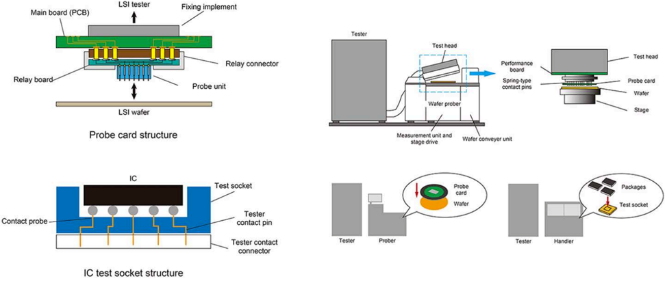
Handier
Test head
Probe card
Wafer
Stage
Packages
Test socket
System Level Tester
Fig. 68: Comparison of testing processes
Tri-Temp handler
1 site in parallel
$$$$ / site
~<2 min TT
electronics
Burn-in
Non-automated oven, thermal,
electronics
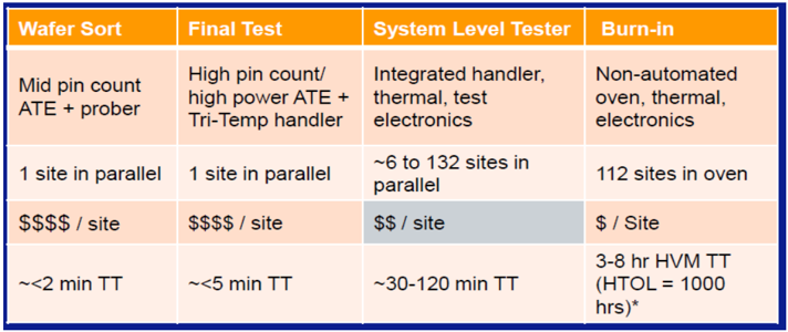
| 1 site in parallel | ~6 to 132 sites in | 112 sites in oven |
|---|---|---|
| $$$$ / site parallel $$ / site | $ / Site | 3-8 hr HVM TT |
| ~<5 min TT | ~30-120 min TT (HTOL = 1000 hrs)* |
Source: Advantest, Nomura research
Probe cards are key components for chip probing
Chip probing: finding the bad dies before they get expensive
Chip probing (CP) is the first electrical test in a chip's production flow - performed before dicing and packaging to screen out defective dies before packaging costs are incurred. To do this, the probe card must make physical contact with the wafer, maintaining stable, uniform contact across tens of thousands of pads and micro-bumps, often under demanding temperature conditions. Testing typically runs in multiple passes (for example, separate hot and room-temperature insertions) and proceeds from basic to deep: first confirming each die's fundamental electrical integrity - opens, shorts, and leakage then verifying the internal circuitry using the chip's built-in test structures, which allow far more thorough fault coverage than external testing alone. For analog and memory circuits, CP goes beyond measurement to active correction: on-chip settings are trimmed and calibrated into spec, and failing memory cells are mapped and repaired through builtin redundant circuits. Advanced packaging has raised the stakes considerably as a single defective GPU or HBM die entering a CoWoS assembly scraps a module worth thousands of dollars (see Testing process changes along with chip complexity ) - so the flow increasingly adds wafer-level stress and burn-in (WLBI), applying elevated voltage and temperature to surface early-life failures before packaging; this practice is most established for HBM and power devices. The end result is a wafer map classifying every die as passing, scrap, or repaired - elevating CP's mission from basic defect screening to guaranteeing that only Known Good Die (KGD) proceed to assembly.
A probe card consists of probe head, interposers, and probe card PCB (PIB)
During the chip probing process, a probe card is used for electrical connection and verification. The probes on the probe head contact with the terminals (pad or bump) on the die of semi wafer/device under test (DUT), sending the signal to the tester to assess its electricity and functionality. A probe card consists of a probe head (with pins), an interposer (also called substrate), and a probe card PCB underneath (Fig. 69 - Fig. 71 ).
Probe head: A probe head is composed of contact probes (needles) and ceramic plates (guide plates). The probe head is the most valuable part in the probe card, it can account for 40-50%+ of the content value of the probe card. Usually, the higher the pin count, the higher the value of the probe head (assuming they use the same kinds of pins). For highpin-count products (30-40k or above), the content value of the probe head can exceed half of the total probe card value. Some probe card vendors will outsource pins (procure pins externally), only providing probe head assembly services (see Fig. 72 ). Different probes suit different ICs and vary by application.
Interposers/Interconnection: Interposer is typically an ABF substrate. Common interposers include MLO (Multi-Layer Organic) or MLC (Multi-Layer Ceramic). The layer tends to serve as a space transformer to bridge probe head and probe card PCB, as its device pitch is much smaller than ATE pin pitch. One major job of a space transformer is to convert/redistribute the coarse pitch of testers to the fine pitch that the device requires.
Probe card PCB: Probe card PCB is at the bottom of the probe card structure, directly contacting the test head of the ATE. Typical layer count for a probe card PCB ranges from 40-70, whereas some engineering/R&D or very small volume projects may exceed 100
Mechanics
PCB
Fig. 69: Probe card structure
Ceramic plates
Probe Head
Tester Side
Stiffener
_ Contact probes
Source: Technoprobe, Nomura research
Backer
PIB
MLO/MLC
Probe unit
Test Head
Probe head unit layers. See more details in Hidden heroes in testing process: test interface boards .
Probe technology on Ceramic
Wafer
Plates of the Probe Heads
Printed Circuit Board (PCB)
Partially outsourced
Vertical Probe Card
Assembly of the ceramid
Ceramic Plates
Plates on which
Probes are then
Board uniti
Probe Head with the probes
Weiding and connection of the Muti Layer produced in the
Organic (MLO) to the Panted Circul board (ru
Fig. 70: Probe card structure with pins
Substrate Unit
Cobra
MEMS
Multi Layer Organic (MLO)
on the market, used in the production process
Source: WinWay, Nomura research
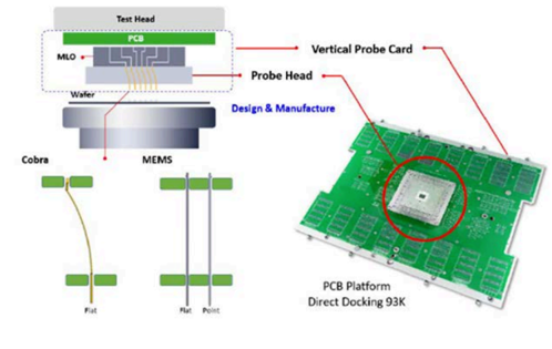
Source: WinWay, Nomura research
Fig. 72: Probe card manufacturing process
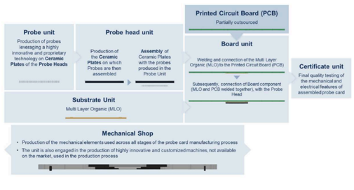
Source: Technoprobe, Nomura research
Different kinds of probe cards; MEMS probe cards are gaining more traction
Probe cards are highly customized products, and usually need to be designed before an IC enters mass production. Usually, a probe card vendor will produce an engineering sample 3-4 months after an IC tapes out, but the chip vendor needs to the contact probe card vendor 1-2 quarters before an IC tapes out (Fig. 14 ). Different ICs fit different types of probe cards, and three major probe cards categories are cantilever probe cards (CPC), vertical probe cards (VPC), and MEMS probe cards. There are still other probe card categories such as membrane probe cards (MPC) for some high-end DDICs or high-frequency RF applications.
CPC and VPC are names of probe card structure, as they actually describe how probes contact the wafers. On the other hand, MEMS is a manufacturing technology for probes. The probes used for a device tend to be highly associated with devices' end applications. Required speed, frequency, device complexity, device density, pin count, and costs all have to be taken into consideration when choosing probes/designing probe cards.
Cantilever probe card (CPC): CPC is suitable for large solder pad/bump size devices. CPC is now mostly used for legacy chips such as logic chips, DDIC, analog ICs, and power ICs. A common type of CPC is an epoxy probe card.
Vertical probe card (VPC): Probes are vertically aligned, and perpendicular to the substrate. VPC is suitable for high-frequency, high-density chips such as SoCs/processors. Some AI chips are still using VPC currently.
MEMS probe card: MEMS is a technology to produce probes, so there could be vertical
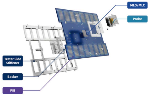
Source: ZENFOCUS, Nomura research
Fig. 71: Probe card structure
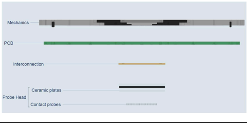
Source: Technoprobe, Nomura research
Certificate unit
Final quality testing o the mechanical and
electrical features of assembled probe card
Troves callulievel out roll lie subot ate nonzumany
Fluves ale veltivally anyteu
MEMS probe cards and non-vertical MEMS probe cards, but current common MEMS probe cards adopted in mass production volume for high-end chips are usually vertical MEMS probe cards, as non-vertical MEMS probe cards cannot meet high pin count and I/O requirements physically for advanced ICs. Therefore, we are only referring to vertical MEMS probe cards when we mention MEMS probe cards in this report. MEMS probe cards are for even finer pitch than classical VPC due to its probe features. As discussed above, MEMS probe cards now account for ~70% of the total probe card market ( Fig. 50 ).
Comparison between different probe cards
- 1) Costs: CPC probe cards are usually cheaper than VPC and MEMS probe cards, and are thus relatively economical.
- 2) Probe mark: As the probes directly contact the devices, it will leave marks on the wafers (i.e. probe marks). CPC probe marks are usually larger/deeper than VPC, and significant probe marks increase the possibility of ruining the wafers.
- 3) Replacement: CPC probes replacement is more difficult than for VPC, and thus incur higher maintenance costs. MEMS probes are sometimes integrated with the space transformer, electroformed or bonded directly on the substrate, making them difficult to be changed. This kind of MEMS probe card doesn't need guide plates.
Fig. 73: Cantilever probe card
Probes cantilever out from the substrate horizontally
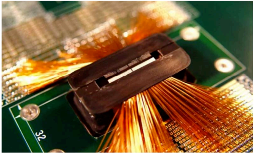
Source: Venture Electronics, Nomura research
Fig. 75: Cantilever probe card
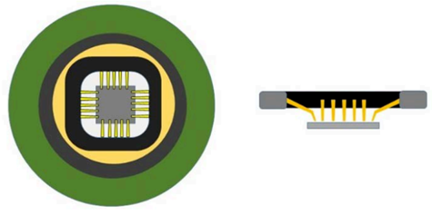
Source: Seiken, Nomura research
Fig. 74: Vertical probe card
Probes are vertically aligned
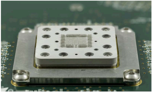
Source: Venture Electronics, Nomura research
Fig. 76: Vertical probe card
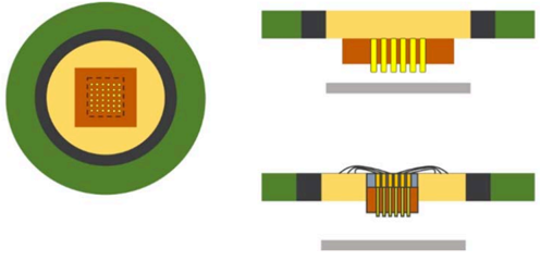
Source: Seiken, Nomura research
lIc arca Wilcie voue viveno Ull MiLlcol cau voltablo
Vertical MEMS probe card
Fig. 77: How different probe cards work
ATE inteface
ATE interface is the area where pogo blocks on ATE test head contacts PIB
High-voltage
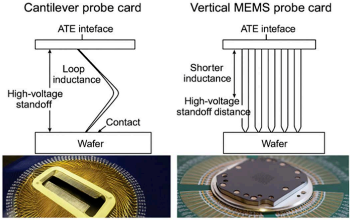
standoff
Source: Elena Venuti, Probe Card Technologies in Advanced Semiconductor Testing for Wide Band Gap Devices, Nomura research
Device pitch shrinkage drives unavoidable usage of MEMS probes
Many forces are driving the shift toward MEMS probe cards: array scale and uniformity (tens of thousands of probes per touchdown with tightly matched spring characteristics, such as in full-wafer memory contact), engineered contact mechanics (precisely controlled force and scrub on delicate low-k pads, and tailored current-carrying geometry for high-power devices), and, at the leading edge processes, pitches below 50 µm where conventionally manufactured probe cards simply cannot deliver the required positional accuracy. Fine pitch virtually mandates MEMS; MEMS, however, is routinely chosen at ordinary pitches for scale and consistency alone.
Device pad pitch is the single strongest driver of probe card architecture, because it simultaneously dictates pin technology, pin count, and mechanical complexity. At coarse geometries (peripheral pads at 60-100 µm pitch typically), simple cantilever needles suffice. Once designs shift to area arrays, like flip-chip C4 bumps at 100-150 µm pitch, angled needles physically cannot reach interior contacts. This forces a transition to vertical cobra pins guided by drilled plates; pin counts jump to 10-50k for large logic dies, and the total contact force reaches tens of kilograms, requiring massive stiffeners. Below 50 µm (e.g., HBM micro-bumps at 40-55 µm), only mask-defined MEMS probes can hold the strict few-micron tip-placement budget. Here, parallelism pushes pin counts to the extreme. See Fig. 78: Typical pitch regimes and corresponding test interface solutions .
Cantilever needle: formed from a bent metal wire, it operates as a flexing beam. When driven against a pad, it creates a "scrubbing" action to break through native oxides. Because of its size and manual alignment requirements, it is strictly limited to peripheral pad layouts and larger pitches (60-100 µm typically). Its primary advantages are low cost and easy repairability, making it the standard choice for analog, power, and legacy devices.
Cobra / vertical buckling-beam pin: Utilizing a short, straight metal wire, the entire pin buckles elastically sideways under pressure. This buckling mechanism delivers highly uniform contact force across non-planar wafer surfaces while producing only a minimal wipe that won't damage solder bumps. Flooring at an 80-150 µm area-array pitch, it is now the industry workhorse for flip-chip CPU, GPU, and SoC testing.
MEMS probe: MEMS probes are microstructures built using semiconductor photolithography and micro-electromechanical techniques. This mask-defined process ensures sub-micron consistency across hundreds of thousands of pins. It produces nearzero scrub (protecting fragile low-k dielectrics) and is the only architecture capable of reaching sub-40-50 µm area-array pitches. Despite its high cost, it is the only viable
"hultlanyoo are mulcauve, bounuareo
Nelweell aujavell leutmolgleo are tanomuon curleo whlere oorutorlo ovellay
Cantilever (peripheral pad)
The buckily-veal mechanism or cordid
Fixing Plate solution for HBM, micro-bumps, and advanced process nodes (Fig. 25 ). Classical VPC probes could not satisfy costs-performance, contact force, and/or probe density requirements, and the probes are not thin and short enough physically for high frequency signal transmission. MEMS probes with extreme fine pitch, better planarity, and extremely shallow probe marks are suitable for high-pin-count, high frequency, high precision devices such as highly advanced processors/AI chips. WLCSP Chip
Note that probe card pin count does not necessarily equal device pin count; how many dies are tested at one time (single-DUT or multi-DUT) will impact total probe card pin count. The equation holds true under single-DUT test (multi-DUT probe card will have more pin count vs. device pin count to test multiple dies at the same time). CPC pin count is usually 1k-2k (although some players can do 7-8k), VPC pin count could be several thousands or ~10k+, and MEMS probe cards pin count could exceed tens of thousands.
Currently, advanced SP AP bump pitch is around 80 µm, and HPC/AI chips pitch is around 100um, thus vertical probe cards are still widely adopted, though the trend is toward MEMS. Based on our industry survey, nVidia is adopting MEMS (sharp tip to contact pad) for AI GPUs/CPUs and networking products, staying at cobra pins (flat tip to contact bump) for gaming GPUs, and ASICs are gradually migrating to MEMS, depending on fabless vendor. Pin count for AI ASICs is also growing, from 20-25k VPC pin sto 30-40k MEMS pins, all the way toward 90-100k+ pins.
Hybrid probe cards adopt mixed-pin technology to incorporate different types of pins on the same probe card to balance cost and performance, such as only adopt MEMS for fine pitch signals and use cobra for surrounded power signal, or adopt cobra for high current signals.
Fig. 78: Typical pitch regimes and corresponding test interface solutions
Pitch ranges are indicative; boundaries between adjacent technologies are transition zones where solutions overlap
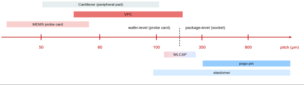
Note: This is a conceptual illustration, not specific to any company or project. Source: Nomura research
Fig. 79: Different kinds of pins
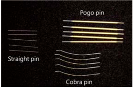
Source: ProbeLeader, Nomura research pills
800
pogo pin
Pressure
Fig. 80: Elastic buckling of cobra pins
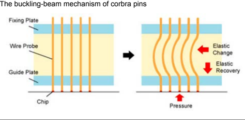
Source: MEMSFLEX, Nomura research
Elastic
Change
Elastic
Recovery pitch (um)
Fig. 81: Key probes technologies
| Pin type | Material / Fabrication | Spring mechanism | Typical applications | Key vendors |
|---|---|---|---|---|
| Cantilever Needle | DrawnW / ReW wire, bent, polished; epoxy-mounted | Bending beam | Analog, power, discrete, legacy devices | MPI, MJC |
| Cobra/Buckling Beam/Wire pin | Machined W-Re alloy wire in guide plates | Elastic column buckling, flat force curve | Flip-chip C4 bumps, CPU, GPU, SoC | Technoprobe, MJC |
| Vertical Pin/Pogo Pin/Spring Probe | Machined barrel with internal micro- spring | Spring compression | Final Test (FT), high-frequency / high-current logic | Smiths, MPI |
| Micro Spring | Proprietary wire core with alloy plating | 3D spring compression | High-performance mixed signal, DRAM / Flash | FormFactor |
| MEMS Probe (inc. Nano Spring) | Photolitho + electroplated Ni-alloy, Rh/PdCo tip | Micro-machined spring / beam | HBM micro-bumps, memory sort, ≤5 nm logic | Technoprobe, FormFactor |
| Membrane Probe | PI film etching with electroformed metal bumps | Contact via elastomer backing | LCD/OLED Display Driver ICs (DDIC), RF chips | MJC, MPI |
| Thin Film Probe | Wafer-level lithography micro- contacts | Tip micro-compliance | 3D-IC, CoWoS, advanced Chiplet stacking | FormFactor, CHPT |
Source: Nomura research
An overview of the IC test process and required hardware
The IC test process consists of package test, burn-in, and SLT
FT is a mandatory procedure , and depending on IC customers' configurations, there could be two or more FT steps during the manufacturing cycle (e.g., nVidia's AI GPUs require two FT steps, one before BIT and the other after BIT). FT is carried out after IC assembly (on substrates, lead frames, or wire bond), and chip packages are capable of accommodating larger input voltages or electric current than bare dies. FT measures electrical properties of chips given pre-programmed inputs to identify product functionality ('pass or fail' is the terminology) and sort functional products by grade (also known as 'binning'), all within the shortest possible time frame (usually hundreds or thousands of seconds) , as chip vendors may want to control test charges (measured by 'hourly rates') which are amortized expenses of costly testers.
We note below three primary parameters form a sequential filtering system in FT for logic circuits, the focus of which is on whether outputs are 'correct'. By contrast, analog/mixedsignal IC testing places more emphasis on the 'measurement accuracy' of select parameters (e.g., linearity and signal-to-noise ratio).
- Direct current (DC) test: The DC test is the first phase in FT and consumes the least time among the three phases. It measures the steady-state electrical characteristics of the chip using direct current and ensures the physical silicon structure is intact. The DC test does not validate logic or speed, however. The primary metrics measured during this phase include: 1) Open/Short test , which verifies that all pins are properly connected to the internal circuitry (no 'open') and that no pins are accidentally welded together (no 'short'); 2) Leakage current , which ensures a pin does not 'bleed' excessive current into the substrate when it is given a specific voltage level; 3) Power consumption , which detects the electric current drain inefficiency; and 4) Output voltage level which confirms the chip can drive signals out at the correct voltage thresholds required to communicate with other components. 1.
- Function test: The subsequent function test is to check whether the logic operation works properly. During the function test, the tester floods the chip with preprogrammed binary inputs (i.e., test vectors) and records the outputs generated by the chip to compare the results against the expected mathematical truth table. Function tests are typically executed at a nominal, conservative clock speeds to isolate pure logical errors from high-speed timing anomalies. 2.
- Alternating current (AC) test: The AC test introduces the critical dimension of 'time', evaluating how the chip performs under dynamic, high-frequency AC conditions and checking the output signals' 'waveform', because a chip might have perfect structure and flawless logic responses at slow speeds. AC test pushes the silicon to its physical limits by measuring sub-nanosecond timing parameters to ensure signals propagate cleanly across the die without corruption. Major test items include propagation delay, setup and hold times, rise and fall times, and maximum frequency. The AC test is also the foundation of 'binning' , sorting out the best-performing chips and lower-tiered ones. 3.
On the other hand, burn-in test (BI) and SLT are optional procedures, but gradually gaining more traction
Burn-in is a reliability screen step, in which chips are operated at extreme temperature (typically 100+ ℃ ) and above-nominal voltage for hours (if not longer). The stress accelerates aging of the chips, forcing latent manufacturing defects to fail during the process (rather than after shipment to customers). BI test is usually mandatory for automotive, aerospace, medical applications, but it is also increasingly important for AI/HPC chips given extremely high content value per package. A high-end GPU requires several hours of BI, compared with FT measuring in seconds, and BI ovens are required in this stage, along with BI boards and BI sockets.
Compared to FT and SLT, where testing processes verify that a chip works correctly currently, infant mortality means working now and failing later. It's impossible for a test coverage to detect a defect that has not yet happened, thus the only remedy is to force it to happen early through stress. Memory and advanced packaging are driving demand for BI test, given that: 1) an HBM stack contains a dozen-plus dies and tens of thousands of bonding interfaces, and one early failure scraps an entire CoWoS module, so screening is shifting earlier to wafer-level burn-in (WLBI) with intensity rising rather than falling; and
•
End CPU TDP
Typical High-
End GPU TDP
8000-
2) datacenter accelerators run in clusters of tens of thousands, where a single early failure interrupts an entire training job, pushing operators' tolerance toward zero. These applications have a high cost of failure combined with time-dependent onset, failure types that BI can address. The increased adoption of BI reflects the rising share of highreliability applications in the semiconductor market.
HPC Chip Power Trends
In design
During SLT, the chip is inserted into a system test board designated by the chip vendor to simulate how it works in a real-world scenario. The test board is a modified version of the actual commercial motherboard that eventually houses the silicon and is equipped with other components such as memory and peripherals. The SLT boots a full operating system such as Linux or Android and runs heavy, asynchronous software workloads to replicate genuine user environments. Throughout the process, SLT measures functional and behavioral metrics rather than raw structural data, including system stability, workload execution throughput, thermal throttling thresholds, and high-speed interface bit error rates (BER). Year Failure modes shifting
SLT has gained traction industry-wide because it exposes defect classes that the preceding stages structurally cannot. DC test, Function test, and AC test are largely deterministic and exercise the device in isolation, at fixed patterns and controlled conditions. They are effective at catching hard, static failures but are poorly suited to intermittent, workload-dependent or interaction-level defects - issues only manifest when multiple IP blocks operate concurrently under realistic power, thermal, and timing stress, or under specific software-induced corner cases. As chip complexity has grown with heterogeneous integration, multi-core coherency, and higher-speed interfaces, these system-level 'test escapes' could result in a larger share of field returns, which has steered SLT from a niche practice in automotive/mobile applications toward broader adoption across compute, AI accelerator, and networking chips, where the cost of a return merchandise authorization (RMA) far outweighs the cost of additional test screening.
The SLT phase is less expensive than FT given no usage of multi-million-dollar testers, but it is very time-consuming and could take minutes or even hours to execute per device. At high volumes, the throughput mismatch could become the binding constraint on SLT adoption, since running every unit through hours of system-level workloads is economically impractical for most product lines. As such, the industry leans toward parallel testing inside automated SLT handlers, and potentially the integration of adaptive testing backed by machine learning algorithms that selectively route only silicons at risk to extended SLT screening while the bulk of the chips proceed through a shortened or standard flow. This 'smart SLT' approach preserves most of the defect-screening benefit while containing the test time and cost overhead, and is emerging as a key differentiator among OSATs and IDMs competing on both quality (defined by defective parts per million, or DPPM) and test cost per unit.
Fig. 82: Chip TDP surge increases importance of burn-in
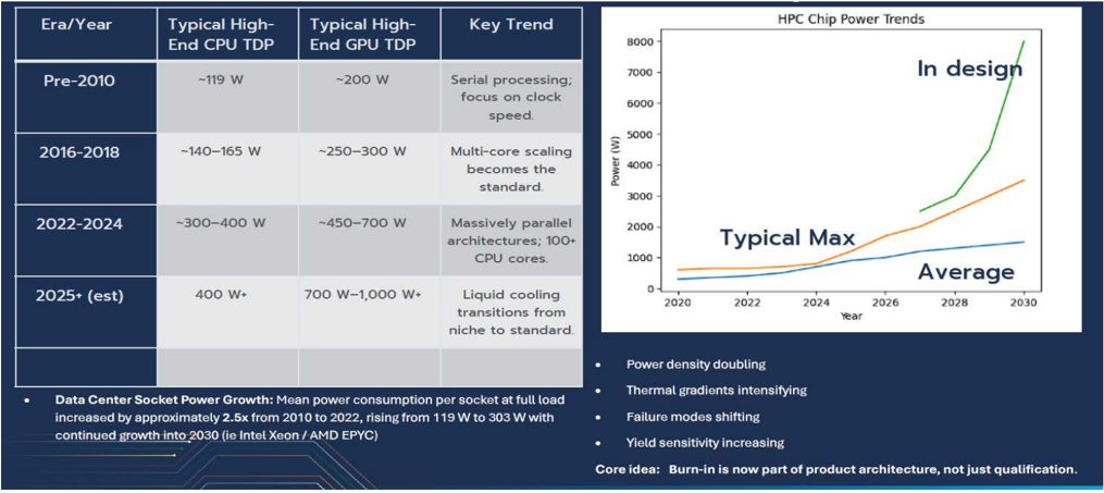
Average
2028
2030
Key Trend
2026
SLT Tester Site
Test
High Speed Interface
(USB, Ethernet, PCle)
Test Protocols
Test Time / Test Cost
Fig. 83: SLT acknowledges that software is part of the system, and recreates the end-use environment as closely as possible DRAM A
Test Site API
Program
Voltage Source
600-2000W package
Liquid cooled in field
Chiplet mesh fabric
Hyperscaler critical
PMIC
Chip Set
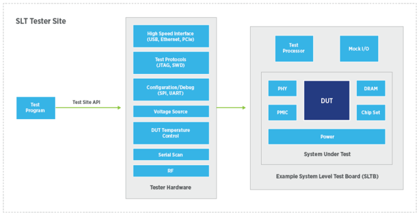
Source: Teradyne, Nomura research
Fig. 84: Decision matrix of testing process
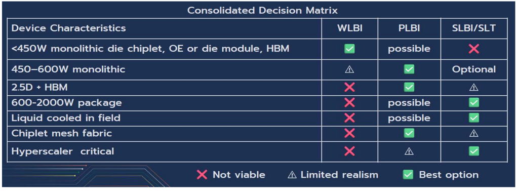
Source: ASEH, Nomura research
Fig. 85: Optimizing cost and quality when deciding testing process
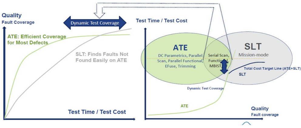
Source: TER, Nomura research
DUT
Consolidated Decision Matrix
WLBI
Test
Processor
Mock 1/0
ATE
X
PLBI
possible
SLT
Serial Scan,
Mission-mode
Functio
MBIST,
Dynamic Test Coverage
A Limited realism possible
Total Cost Target Line (ATÉ+SLT)
possible
SLT
Best option
Quality
Fault coverage
SLBI/SLT
Optional
Testing
Interposer Size
2026 TSMC, Ltd.
Cowos-s
CoWos-L/R
CoWos-s
1.5-reticie
4 HBM2
N16 SoC
'16
Adaptive
CoWos® Enables Al Compute Scaling
Functional Testing
(ATE)
CoWoS® Enables Al Compute Scaling
• World's largest 5.5-reticle size CoWo in production with >98% yield in 2026
• Continue scaling with larger interposer size for growing Al compute demand,
Product
Ship with 14-reticle (20xHBM) ready by 2028 and >14-reticle (24xHBM) by 2029
Fig. 86: Adaptive SLT could further reduce the overall cost (time) of test
A16 SoC/SoiC
212 HBM4E|
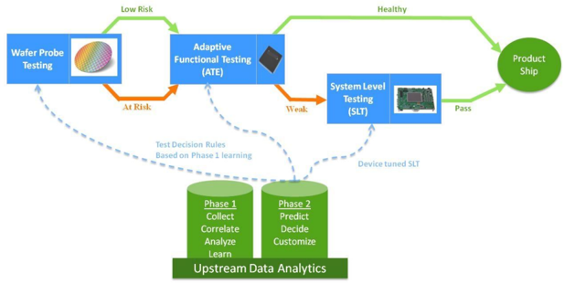
Source: AEM, Nomura research
Handlers are more than mechanical arms
While IC test handlers alone might initially seem like simple mechanical automation which is often oversimplified as mere robotic arms picking and placing devices under test, the reality under the hood is a sophisticated combination of high-precision micro-mechanics and solid knowledge in thermal physics.
We highlight that FT handlers could eventually undergo mechanical redesign and OSATs have to upgrade the tools if chip packages expand to a certain bar. Thus far, AI/HPC is the primary driver of package footprints. With logic dies already approaching a physical limit closer to the reticle size, nVidia and other AI accelerator makers understand incremental performance gains must come at the sub-system level rather than the chip level, and consequently are targeting to stack more logic dies and more HBM cubes onto interposers to construct a more powerful computing chip system. nVidia has moved from Ampere/Hopper (both 2x reticle-size interposer), to Blackwell in 2024 which houses two reticle-size compute complexes and eight HBM cubes on a 3.3x reticle-size interposer, and soon to Rubin in 2026E which houses two reticle-size compute complexes, two I/O dies, and eight HBM cubes on a 5x reticle-size interposer.
We believe the horizontal expansion of AI chip footprint is unlikely to halt as TSMC continues to unfold its CoWoS roadmap to introduce larger interposers (and therefore larger IC substrates underneath). According to TSMC, it is bringing 5.5x reticle size CoWoS into production in 2026 with a >98% yield. Previously TSMC suggested its 9.5x CoWoS-L with SoIC and 12 HBM stacks would enter production in 2027E (Fig. 87 ; Tech Symposium 2025 ), and during the symposium this year, the company extends the roadmap to 14x reticle size CoWoS (20 HBM stacks) production by 2028 and aims for >14x reticle size CoWoS (24 HBM stacks) in production by 2029 (Fig. 88 ).
Fig. 87: TSMC's CoWoS roadmap laid out in 2025 Technology Symposium
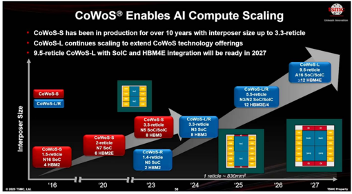
Source: TSMC, Nomura research
Fig. 88: TSMC updates its CoWoS roadmap
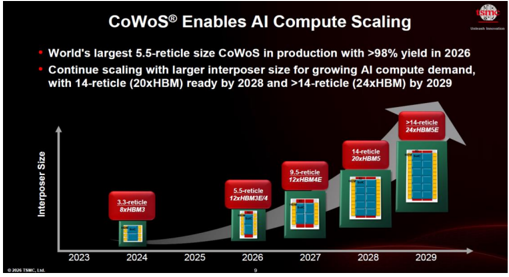
Source: TSMC, Nomura research
Healthy
2025
5.5-reticle
12xHBM3E/4
2026
9.5-reticle
12xHBM4E
2027
14-reticle
20xHBM5
2028
>14-reticle
2029
258x537.6mm and the right one measures to 380x387.6mm
L. SIDE
VIEW
We note 'the bar' is correlated to 'how many chip packages that a matrix tray can accommodate' during the FT stage. A matrix tray is a plastic carrier that holds IC packages in a rigid grid of rows and columns, and the robotic arm of a handler will move the vacuum suction nozzle over the input matrix tray, suctions up untested chips (DUT), and places DUT into the test socket. The dimension of the tray generally conforms to the standard proposed by the Joint Electron Device Engineering Council Solid State Technology Association (JEDEC in short). The current standard tray is specified at 135.9x322.6mm , but if a chip package measures 120x125mm, one standard tray can carry only two pieces of DUT. The JEDEC acknowledges the industry trend of moving toward larger package footprints (notably in recent years, propelled by AI/HPC), and has added two new types of tray (also known as 'mega tray') in recent issues: 258x537.6mm and 380x387.6mm . CH
Based on our understanding, Hon has progressed the development of large-package handlers based on the new JEDEC standards given its substantial exposure to AI/HPC applications (~80% of tool orders in 1Q26). The current planning is to begin shipments of tools capable of handling >120x150mm packages in 2H26E, and a handler solution for 250x250mm package in 2H27E, to position itself early for the next round of handler upgrades. Hon also targets to add more automation functionalities for better integration with unmanned factories (e.g. overhead hoist transfer [OHT] and autonomous mobile robot [AMR]) to boost throughputs. Our 'napkin math' indicates that a 120x150mm package could house an interposer sizing up to 10-11x reticle, which ties with TSMC's CoWoS roadmap in 2027-28, whereas our supply chain checks have not yet picked up such a large AI chip in the pipeline.
Fig. 89: IC matrix tray
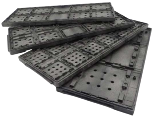
Source: Sunrise, Nomura research
Fig. 90: JEDEC adds two new types of tray to address larger package size
The left one is the current standard tray (135.9x322.6mm), and the one in the middle measures to 258x537.6mm and the right one measures to 380x387.6mm
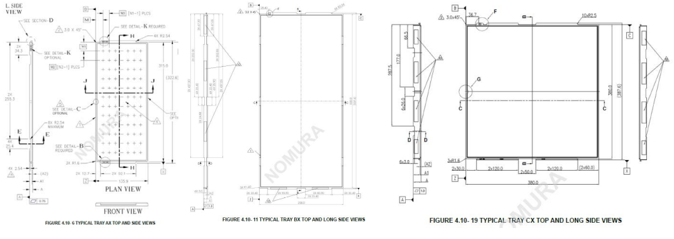
Source: JEDEC, Nomura research
Intel's EMIB might open a new window for large AI chip test demand. We believe some AI ASIC customers might have started evaluating Intel's EMIB-T (embedded multi-die interconnect bridge with TSV) as a logic+HBM integration alternative because of concerns about insufficient capacity support at TSMC. According to Intel, EMIB-T targets HBM4/4E and logic chiplet interconnectivity with the lowest possible cost, and the company's roadmap is to scale to the integration of >8x reticle size total top silicon area on a ~120x120mm substrate by 2026E and >12x reticle size top silicon area on a >120x180mm substrate by 2028E (Fig. 91 ). If successful, Intel's EMIB-T might open a new demand window for large AI chip testing.
We think Google's potential reliance on Intel's EMIB-T for the next-generation TPU v9 (partnering with MediaTek) could be a critical litmus test for Intel's advanced packaging capabilities. Based on our supply chain analysis, this signpost project will feature a substrate body size within 120x120mm (see the floorplan in our report ), not yet necessitating the transition to mega tray configuration.
B-1
A 3.0045 - 1
JIRLE
230.0.
24120.0
12-40 0)
FIGURE 4.10- 19 TYPICAL TRAY CX TOP AND LONG SIDE VIEWS
-4x
Reticle
Fig. 91: EMIB roadmap
8
12
-8x
-120x120
HBMs size
intelfoundry
EMIBs
Reticle size
Package size
12
HBMs
20
EMIBs
-12x
Reticle size
2028 +
-120*x180+
24
Package size
HBMs
38
EMIBS
40 x+
Reticle size
Future
-241x240
Package size
200+
EMIBS
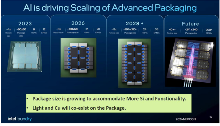
Source: Intel, Nomura research
Another driver of upgrades comes from AI/HPC customers' migration to more powerful ATC (greater cooling capacity), since the sub-system performance gain from more dies in a package comes at the cost of more stringent thermal requirements.
Using nVidia AI GPUs as an example, the maximum TDP of Blackwell Ultra (B300) is 1,400W, which can be supported by Hon's ATC3.5 (cooling capacity of up to 2,000W) during the FT stage. However, we think the TDP of Rubin (R100) may start from 1,800W, leaving little margin for ATC3.5 and likely initiating an upgrade to ATC3.6 (up to 3,000W). Admittedly, comparing TDP to ATC maximum cooling capacity is sometimes more biased than 'power density' (also better known as 'heat flux' in thermal physics), because TDP only tells us 'how much heat is generated' and power density/heat flux provides us 'how concentrated the hotspot is' and 'how fast the heat transfer is'.
nVidia will be more aggressive in chip specs by stacking a reticle-sized GPU die on top of another for the Feynman platform, the first-ever GPU-on-GPU SoIC stacking (report ), which would lead to higher computational power even with limited growth in interposer reticle stitching size (c.6x reticle, see footprint in Fig. 93 ; up from c.5x in Rubin). Such a practice theoretically exacerbates thermal dissipation challenges, and we expect it could trigger a migration to more powerful ATC3.7 . According to Hon, it has ATC with a max imum cooling capacity of up to 7,000-8,000W ready, and is working on engineering en route to >10kW (Fig. 94 ).
The similar rationale applies to SLT handler as well. We believe SLT handler upgrades are primarily driven by the tight coupling between the handler's mechanical and thermal interface and the physical design of each new AI chip platform. Unlike FT, which tests a packaged die in a relatively standardized form factor, SLT validates the chip at the full system or module level , indicating socket pin count, board layout, power delivery, and thermal load are all specific to that generation's module configurations. Altogether will further compound the changes for more challenging hand-in-hand engineering efforts by SLT handler makers with end customers.
Dummy
HBM4
HBM4
HBM4
Dual-temp
HBM4
(25~150°C)
Power Density
HBM4
XCD
(N2)
HBM4
Tri-temp
(-80~180°C)
HBM4
Fig. 92: Floorplan of AMD MI455 and cross section
(N2)
Reconstituted interposer (5.5x ret.)|
B series
R series
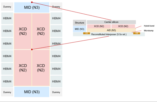
Source: Company data, Nomura research
SiC thermal plate to function as an intergrated silicon carrier (fill up the
1/O
HBM4E
HBM4E
1/0
Fig. 93: The floor plan and cross-section chart of nVidia's Feynman GPU
SiC thermal plate to function as an intergrated silicon carrier (fill up the height gap in between GPU and HBM) and thermal interface material (TIM)
HBM4E
Structure
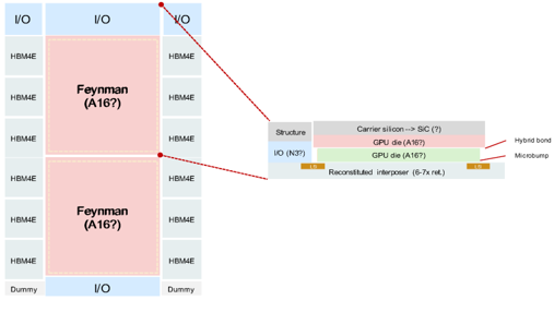
Source: Company data, Nomura estimates
Fig. 94: Hon's ATC roadmap to address greater TDP by AI/HPC chips
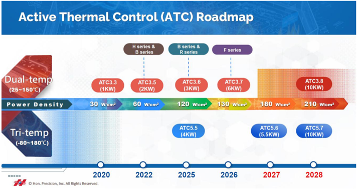
Source: Company data, Nomura research
Theoretically the tier-one ATE maker Advantest could have enjoyed a natural installed base advantage in test handlers sales since handlers are used along with tester, and Advantest has advanced technological capabilities in mechatronics to optimize the coordination of handlers and testers. This is particularly valid in memory testing, where the testing relies on extreme parallelism (i.e. high throughputs on fairly standardized interfaces). Advantest was able to build up a large handler market share in the past when it leveraged its memory tester installed base, before it gradually lost ground to emerging memory handler specialists like Techwing (089030 KS, Not rated).
Hon's ATC/handler business serves primarily logic semi (it only had 1-2% of tool orders from memory in 2025), where the inherent advantage of Advantest disappears entirely. Logic packages are of high varieties than commodity memory, featuring varying physical dimensions, ball counts/pitches, etc., and this requires deep, early-stage collaboration during the new product introduction (NPI) phase as well as close-knit communication with specialized test interfaces (load boards and sockets) to build bespoke mechanics inside handlers. Specialized handler makers such as Hon can thrive on engineering fluidity. By contrast, Advantest does not devote many resources to tailor handlers given that handlers are essentially 'sidekicks' (1-2% of total revenue) and IC testers are its core business lines. This may also explain why Teradyne does not have its own handler business units given a great exposure to logic testing.
Handler customization is especially important and necessary in the realm of AI/HPC and ASICs due to large die sizes, complex multi-die packaging (e.g. 2.5D/CoWoS) and ultra-
HBM4
Microbump
F series
Dummy
20
15
10
5
0
high pin counts, and Hon is an expert in these areas (72% of tool orders from AI/HPC and ASICs in 2025). Hon engages directly into the embryonic development phases of AI/HPC and ASICs through tight NPI collaborations with end customers backed by a robust IP portfolio of more than 600 patents filed globally across thermal control, high-throughput, and active optical inspection (AOI), and ships early configurations to end customers' R&D labs for engineering validation and joint developments. We summarize Hon's NPI status (data as of 2Q25) in Fig. 95 .
Furthermore, the handler is more than a sheer mechanical sorter in AI/HPC testing as the accompanying ATC becomes an active execution environment. Hon's dual-temp and tritemp ATC cover a broad spectrum of operating temperatures and cooling systems (liquidcooling, refrigerant-cooling, and air-cooling), and the company continues to move forward in capabilities with an extended roadmap to 7,000-8,000W readiness and >10kW in the engineering pipeline (Fig. 94 ). A clear visibility of ATC roadmap and well execution, in our view, puts Hon in a more favorable position for AI/HPC clients looking to initiate new chip development.
Fig. 95: Hon's NPI status by application and end-customer location
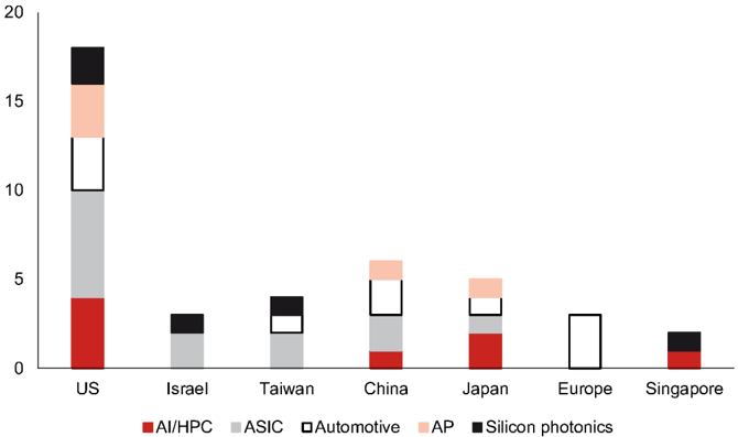
Note: Data as of 2Q25.
Source: Company data, Nomura research
Fig. 96: Comparison of major global tester and handler makers (ex-China)
| USD mn | Headquarter | Market cap | 2025 revenue | Revenue mix | Revenue mix | 2025 GM | 2025 OPM | 2025 net profit Tester | 2025 net profit Tester | Handler |
|---|---|---|---|---|---|---|---|---|---|---|
| USD mn | Headquarter | Market cap | 2025 revenue | Tester | Handler | 2025 GM | 2025 OPM | Handler | ||
| Hon. Precision (7769 TT) | Taiwan | 33,781.0 | 971.3 | n.a. | c.80% | 56.5% | 49.7% | 396.6 | n.a. | FT 70-80%, SLT 20-30% Mostly logic/analog |
| Chroma ATE (2360 TT) | Taiwan | 24,332.8 | 908.4 | 10-15% | 20-25% | 61.5% | 32.5% | 375.2 | Mature logic/analog | FT 30-40%, SLT 60-70% Mostly logic/analog |
| Advantest (6857 JP) | Japan | 123,945.2 | 6,902.1 | 82% | <5% | 62.4% | 39.7% | 1,927.8 | 80% Logic/Analog 20% Memory | FT, SLT Mostly memory |
| Kanematsu (8020 JP) | Japan | 2,157.8 | 7,062.3 | n.a. | <5% | 15.7% | 4.4% | 215.8 | n.a. | FT, SLT (from Seiko Epson) Mostly logic/analog |
| TESEC (6337 JP) | Japan | 75.5 | 37.6 | 45% | 36% | 37.8% | 5.7% | 2.0 | Mature logic/analog Discrete | FT (from Yokogawa) Mostly logic/analog |
| Cohu (COHU US) | US | 2,414.9 | 453.0 | ~40% | ~40% | 43.3% | 0.5% | (10.1) | Mature logic/analog | FT, SLT Mostly logic/analog |
| Teradyne (TER US) | US | 50,462.1 | 3,190 | 75% | 15% | 58.3% | 22.3% | 632.1 | 80% Logic/Analog 20% Memory | SLT Mostly logic/analog |
| Techwing (089030 KS) | South Korea | 1,222.7 | 112.0 | n.a. | 36% | 42.2% | 10.0% | 6.6 | n.a. | FT Mostly memory |
| SEMES (unlisted) | South Korea | n.a. | n.a. | n.a. | n.a. | n.a. | n.a. | n.a. | FT Mostly memory | |
| AEM (AEM SP) | Singapore | 2,137.2 | 305.6 | 30% | 25.7% | 5.9% | 13.0 | Mature logic/analog | FT, SLT Mostly logic |
Note: Market cap data as of July 17, 2026.
Source: Company data, Bloomberg Finance LP, Nomura research
Socket
Device Under Test (DUT)
The role and structure of testing sockets
Sockets are used in all three processes (FT, BIT, SLT), and a socket tends to combine electrical, mechanical, and thermal aspects into a single structure. The socket is an interface between the DUT and the test equipment, sitting between the DUT and the load board. A socket requires precise contact resistance and shielding effectiveness measurements to ensure reliability. The signal is transmitted from PCB (load board) to device and return to PCB. The DUT is aligned to the floating plate on the socket, and the floating plate aligns the springs to the center of the solder ball (BGA)/pads(LGA). A handler pushes the DUT into the socket.
Core components of a socket include:
Socket lid/clamshell/latch: usually necessary in burn-in sockets (when sockets are lidless, the handler's plunger will press the device down). The lid physically presses the IC package done into the contactors and ensures uniform force distribution across all pins.
Housing/socket body: the main structure of a socket, usually a precison-machined or molded insulating frame (using advanced engineering plastics). For coaxial test sockets, the housing is made of machined aluminum or brass. In some cases, ceramic or glassfilled composites are utilized.
Alignment plate/floating guide: to hold the DUT in place and keep the solder balls/pads aligned with the socket's contact pins.
Thermal features: Sockets sometimes incorporate a thermal control unit (TCU), directly pressing on DUT for heat dissipation.
Contact elements: the pins or elastomer that carry signals, a conductive pathway to bridge the chip to PCB.
Fig. 97: Typical socket construction
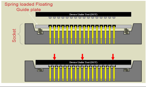
Source: PTSL, Nomura research
Different sockets are adopted in FT/SLT and BI processes
FT and SLT sockets are relatively similar, and thus market research institutions tend to combine the two types together when calculating market size, while leaving BI sockets as another category (see Socket market size relatively stable with shifting market share ).
Test sockets are used for relatively short-term testing cycles, and optimized for signal accuracy, high-frequency capacity, high insertion durability, and minimal contact resistance. On the other hand, given the longer testing time and tough testing environment, BI sockets need to bear extreme temperature and electrical stress physically and are equipped with thermal-management solutions. The BI process will test a substantial amount of chips at the same time (massive parallelism), thus BI sockets sacrifice speed/frequency and signal integrity, resulting in lower costs and a much simpler manufacturing process. SLT requires chips to run in a mimic environment as real use cases, thus the socket needs to run all required functions. As SLT testing time is also longer than for FT, parallel testing is also required to increase throughput, and thus more SLT opportunities benefits socket suppliers in terms of volume.
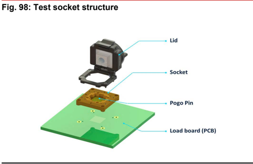
Source: DediProg, Nomura research
- Lid
• Socket
• Pogo Pin
- Load board (PCB)
After packaging
Fig. 99: Different types of sockets in different testing steps
Introduction
Products
SLT
Burn-in Test
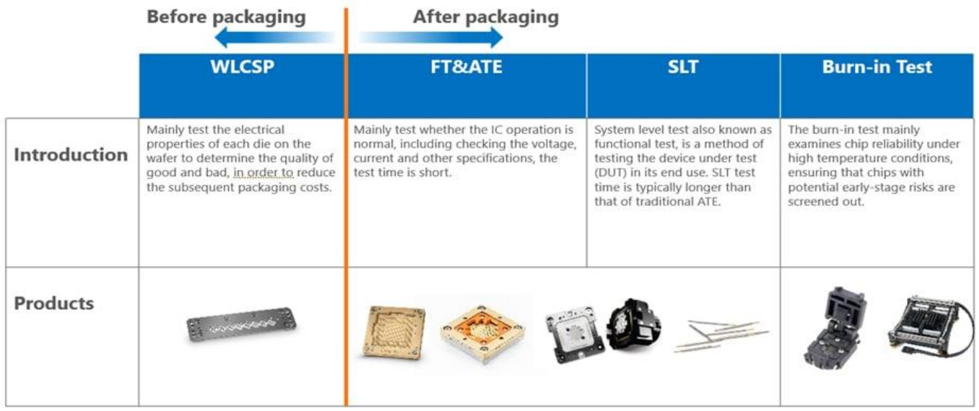
| Mainly test the electrical properties of each die on the | Mainly test whether the IC operation is normal, including checking the voltage, current and other specifications, the System level test also known as functional test, is a method of testing the device under test The burn-in test mainly examines chip reliability under high temperature conditions, | Mainly test whether the IC operation is normal, including checking the voltage, current and other specifications, the System level test also known as functional test, is a method of testing the device under test The burn-in test mainly examines chip reliability under high temperature conditions, | Mainly test whether the IC operation is normal, including checking the voltage, current and other specifications, the System level test also known as functional test, is a method of testing the device under test The burn-in test mainly examines chip reliability under high temperature conditions, |
|---|---|---|---|
| wafer to determine the quality of good and bad, in. order.to reduce the subsequent packaging costs. test time is short. | (DUT) in its end use. SLT test time is typically longer than that of traditional ATE. | ensuring that chips with potential early-stage risks are screened out. |
Source: Smiths Interconnect, Nomura research
Two major contact elements - spring probes and elastomer
The contact elements in a socket predominately indicate pogo pins and elastomer (silicone rubber), while cantilever pin sockets are used mostly for legacy product/memory testing (relatively rare).
Spring probe (or pogo pins) are the most common type of probes used for AI chips currently, and common base materials for spring probes include brass, bronze, copper, plated nickel silver, and gold. All components are gold finished for excellent electrical conductivity, durability, and corrosion protection. Spring probes are spring-loaded electrical contacts, due to inclusion of a spring. A constant normal force on target surfaces can enable consistent electrical performance during testing. A typical pogo pin consists of plunger, barrel, and spring (Fig. 100 - Fig. 101 ). When force is applied, the spring compresses and the plunger moves inside the barrel. Pogo pins have a longer lifespan, and individual probe replacement is possible, while the physical signal path is longer. The shape of the tip on a pogo pin is application-specific: crown/cup/concave tips are standard for BGA solder balls or WLCSP packaging, flat or round tips match LGA or QFN packaging, and pointed tips fit coarse pads or via/through-holes (Fig. 102 ).
Elastomer is another contact element alternative. It replaces mechanical springs with a composite material - non-conductive silicone rubber matrix embedded with conductive particles (rubber is an insulator). When the IC is pressed down, the particles contact each other, and creating a conductive vertical path. Elastomer causes near-zero mechanical damage due to its even distribution of stress, and creates a short signal path, also improving signal integrity for high-frequency/RF/mmWave testing. However, its lifespan is shorter, and replacement would have to be more frequent and less flexible (whole layer).
WinWay's proprietary HyperSocket is a mix of pure spring probe and elastomer solutions (we provide more details in the company section of this report).
Some common related tip type.
-A concave
-J round
-D spherical round
-E Conical
-F Flat
-V 4 - point crown
-H 9 - point crown
-T Pyramid
As little as 3 components. But some probes have 30+
BGA
Fig. 100: Spring probe is also known as pogo pin
• The plunger is the moving part that makes contact with the DUT thru the. It is biased to ensure contact
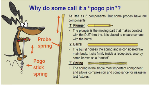
DUT side
DUT Side
DUT
Plunger
BGA
BGA
BGAS CBGA
Fig. 101: Spring probe introduction
Spring
PCB side
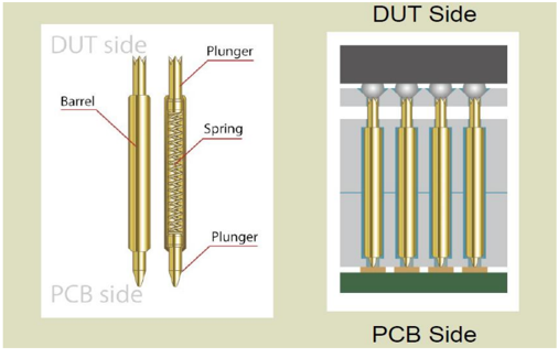
Source: Uyemura USA, Nomura research
Fig. 103: Pogo vs elastomer type of socket
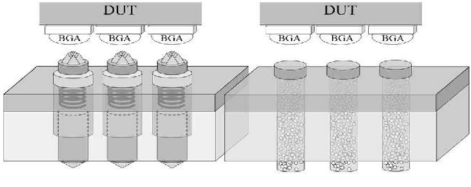
Source: Junyong Park, Modeling and measurement of high-bandwidth and high-density silicone rubber socket for 100Gbps transceiver IC test, Nomura research
Source: Junyong Park, Modeling and measurement of high-bandwidth and high-density silicone rubber socket for
Source: INGUN USA, Nomura research
Source: INGUN USA, Nomura research
Fig. 102: Different packaging methods suit different probe tips
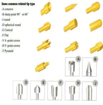
Source: SFENG, Nomura research
Coaxial sockets are now mainstream for advanced logic chips
A coaxial socket is actually a structure, not a type of contact element. In this architecture, each signal contact is enclosed in a dielectric insulator, and then runs inside a grounded metal shield. The structure prevents crosstalk and noise, and matches the required impedance. Major AI accelerators/CPUs now predominantly use coaxial socket architectures, given the better signal integrity, high-speed compatibility, high-frequency, high power-consumption logic and RF/networking chips (Fig. 104 - Fig. 105 ). Coaxial sockets utilize nearly 100% pogo pins (coaxial elastomer sockets exist, but are very uncommon).
Non-coaxial solutions use standard pogo pins or unshielded pins, and common elastomer sockets are non-coaxial, as the physical path is already short.
DUT
BGA
wiew.com (Smiths Intercorne
P G
Air gap
Dielectric
• Top howsing
Metal housing
GND pin
Fig. 104: Coaxial socket structure
Power and
Ime frequency pin
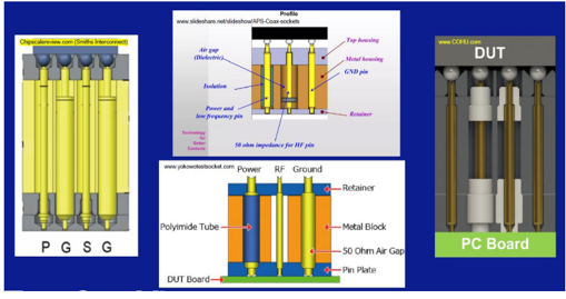
Source: Modus Test, Nomura research
Hidden heroes in testing process: test interface boards
All contact elements require a mounting surface - which necessitates the use of a Test Interface Board (TIB)
The terminology around Test Interface Board (TIB) is a frequent source of confusion. Specifically defined (by Technoprobe, Fig. 106 ), a Device Interface Board (DIB) is the load board used in the final testing of the packaged parts, while a Probe Card Interface Board (PCIB) is used to identify the sub-assembly of the probe card PCB (plus a spacetransformer substrate, whenever needed) before the probe head is mounted (see Probe card accounts for 40%+ of the test connectivity market for more details on probe card structure.)
A Probe Interface Board (PIB) , by contrast, is not a mandatory element of the signal chain: it is an optional adapter board inserted between the ATE tester head and the probe card under certain tester configurations - for example, to remap pogo-tower resources or bridge platform incompatibilities - and is absent entirely when the probe card is natively designed for the tester. However, "PIB" is now often used loosely on the wafer-test side to refer to the probe card PCB now (i.e., PCIB).
Recall that the signal path in CP and FT should be:
- For wafer-level-testing: ATE test head (pogo tower) - PIB (not always present) Probe card (probe card PCB + interposer + probe head) - wafer ·
- For packaging testing: DIB - socket - contact elements - chip ·
While DIBs have a relatively smaller value compared with probe cards and sockets, they accounted for ~17% of the total test connectivity market in 2024-2025, at USD900mn-USD1bn (Fig. 48 - Fig. 49 ), growing from USD500mn+ in 2020, according to TechInsights. Yole further projects a 4.9% revenue CAGR (2025-30E) for test interface boards, the lowest growth rate among all test interface categories (Fig. 47 ).
www.COHU.com
DUT
• DaVinci Gen V Socket Structure
IC Device
IMe Material
Fig. 105: Example of high-performance coaxial socket
Cartridge Top
Spring probes
Source: Smiths Interconnect, Nomura research mm
Best
4.70
mm
(Test)
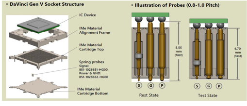
Source: Smiths Interconnect, Nomura research
• Illustration of Probes (0.8-1.0 Pitch)
Fig. 106: Test Interface Boards in testing process
Probe Cards & Tester Components
FINAL TESTING
Final Test Components
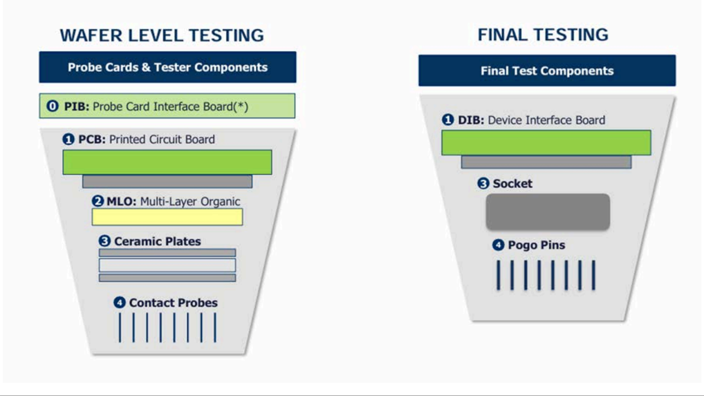
Source: Technoprobe, Nomura research
Probe card PCB, burn-in board (BIB), and DIB/load board are distinct components
Test Interface Boards (TIB)- including probe cards, load boards, and burn-in boards serve as the vital electrical bridges during qualification, and they differ radically from the conventional PCBs that host finished chips. The core reason is routing burden. A conventional product board routes one system's signals. A test board must route every tester channel - including thousands of signals, power, and ground connections for an AI accelerator- from a large tester footprint down to a die or socket footprint measuring just a few centimeters across, all impedance-controlled and length-matched. As a result, a chip's test board typically requires several times more layers than the final product in which that chip will be integrated.
Probe Card PCB: Operating at the wafer level, the PCB is the large round or square board onto which the probe head and stiffener are mounted; it fans out signals from the tester's pogo tower to the fine-pitch probe area. Since PCB fabrication alone cannot bridge from millimeter-scale board features to the fine pitches of devices, most advanced probe cards incorporate a space transformer - either a multi-layer ceramic (MLC) or multi-layer organic (MLO) substrate - positioned between the PCB and the probe head to complete the pitch translation.
Load Board / DIB: Also called a DUT board, it serves as the critical electrical interface between the ATE tester head and the handler/contactor socket holding the packaged IC. Used in the package-test flow at OSATs, the socket sits on top, while thousands of tester channels are routed underneath. For ICs with high-speed interfaces, load boards carry strict impedance and length-matching requirements so that signals are transferred with minimal distortion. Note that a DIB is delivered as an assembled, electrically verified unit populated with thousands of components rather than just a bare board.
Burn-in Board (BIB): The BIB serves as a robust mechanical and electrical fixture for reliability screening. Dozens of burn-in sockets are soldered onto a single large-format board - often spanning several hundred millimeters to maximize oven throughput which is then loaded into chambers and subjected to extreme high temperatures for hours or days to identify early-life failures. The critical requirement is not signal speed but rather the ability to withstand prolonged and repeated thermal stress.
Probe card PCBs and load boards use the same top-grade materials, but their challenges differ fundamentally. The probe card PCB's fine-pitch burden is absorbed
by the space transformer, so the board itself can use conventional through-hole, singlelamination construction. Its primary challenges are extreme layer count and flatness (tens of thousands of probes pressing down simultaneously, even surface deviations of a few tens of microns can cause contact failures, and the board must hold its shape on a heated chuck.) The load board has no such intermediary because socket contacts land directly on the board surface. Escape routing, GHz impedance control, heavy current delivery, and thousands of assembled components all compete for the same layer budget, often necessitating blind/buried vias and sequential lamination. Its acceptance criteria are electrical : impedance tolerance, signal loss, and channel calibration. The burn-in board carries slow signals, and modest layer counts; its challenge is neither electrical nor precision but rather heat endurance and cost - maintaining structures through days in ovens with temperatures of above 125°C, shipped in dozens to hundreds per program, and competing on durability and price.
Fig. 107: TIB comparison
Load board is the most complicated in terms of design
| Dimension | Probe card PCB | Load board (DIB) | Burn-in board (BIB) |
|---|---|---|---|
| Test stage | Wafer test (CP) | Final test (FT) | Burn-in screening |
| Core challenge | Pitch translation (µm- class), flatness | Signal integrity + heavy power delivery | Days of dimensional stability at 125-150°C |
| Layer count | 40-70+ | 30-60+ | ~6-20 |
| Material focus | Low-loss hybrid, extreme flatness | Low-loss hybrid + back- drilling | High-Tg FR4 / PI (heat first) |
| Signal speed | High | Highest (GHz at-speed) | Lowest (kHz) |
| Distinctive structures | Space transformer (MLC/MLO) | Heavy component assembly, pogo tower interface | Dozens of sockets, large format |
| Unit price | High | Highest (six figures at the top) | Lowest (volume-driven) |
| Key vendors | CHPT, Technoprobe/Harbor | AIS, CHPT, Keystone | TSE, Daeduck, Fastprint |
Source: Nomura research
Difference between common system-level PCB and TIB
The most fundamental difference between the two types of boards is decided at the design intent itself. A conventional PCB (system-level PCB or product board) is designed for production: its mission is to perform one fixed job reliably over the product's lifetime - soldered in, powered up, used for years - so the design goal is to minimize unit cost and maximize yield and throughput while meeting the product spec, with one design replicated hundreds of thousands to millions of times. A TIB is designed for test: it is not a product but a measurement instrument - its mission is to extend the tester's capability to the chip's pins without distortion, and to stay accurate through hundreds of thousands of insertions or hours to days of high-temperature baking. Its design goals are therefore prioritizing performance and precision first, rather than cost considerations, as one design is typically built only a handful of times (much less than mass production volume). Any excess loss, impedance deviation, or thermal warpage in the board itself would result in misjudgements (good chips being classified as bad, or passing bad chips).
Process-wide, TIB adopts subtractive lamination and mechanical drilling similar to traditional PCBs. However, for TIBs, the aspect-ratio requirement for drilling is much higher, and high-end TIBs usually require back-drilling. Material-wise, consumer electronic PCBs use standard FR4 given the lower cost, and high-end servers/switch boards use low-loss laminates (M6/7 series or above) for high-speed signals. Probe card PCBs and load boards adopt a hybrid structure combining low-loss and FR4 materials (uses premium materials only for high-speed layers). In contrast, for BIBs, speed does not matter, but as it has to withstand high temperatures, it usually adopts high Tg FR4 or polyimide (PI). Essentially, BIBs trade electrical performance for enhanced thermal features.
Layer count-wise, it is challenging for a TIB to shrink in size (to accommodate the tester's large footprint and provide mechanical strength), so it typically gains routing space by increasing thickness and layer count.
Common smartphone motherboards adopt 8-12 layers HDI, PC boards could be 6-10 layers, general server is 16-20 layers, while AI servers/switch could be further higher (2040+). A TIB must funnel thousands of tester channels down to the chip footprint, all impedance-controlled and length-matched; thus, a chip's test board typically contains several times more layers than the final product in which that chip will be integrated.
mechanical drilling / laser drilling
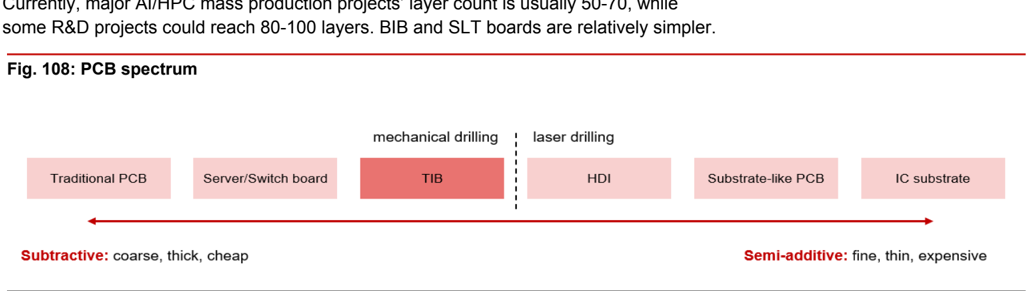
Source: Nomura research
Key players and dynamics in TIB market
Though TIB suppliers and volume board fabricators both belong to the PCB industry, their business models differ fundamentally. Volume fabs replicate one design millions of times, competing on yield and scale at 10-30% gross margins (depending on layer count and complexity); a TIB supplier runs a full cycle from design, fabrication, to assembly and calibration (while some players outsource manufacturing, operating a fabless-like business model). The vendor sells the engineering solution rather than the board itself, with gross margins commonly reaching 30-50%. Every device generation and package change requires a fresh board design, creating recurring procurement demand untethered from any single product's volumes.
Two major types of suppliers in the TIB market - captive and merchant
The captive camp - owned by ATE/probe giants: The test-equipment majors have pulled TIBs in-house in recent years: Advantest consolidated R&D Altanova (boards) and Essai (sockets) into its AIS segment, tied to its V93000 tester ecosystem and focused on flagship-processor load boards; Technoprobe (the probe card leader) acquired Harbor Electronics and Teradyne's former DIS board business, keeping probe card PCB flatness yield under its own control. The captive's niche is on co-design and customer lock-in: tester/probe head and board are developed as one, tuned for maximum performance, while keeping customers inside the parent's ecosystem. However, a customer running Teradyne testers may hesitate to buy boards from Advantest.
The merchant camp - independent specialists: Unaligned with any tester brand and open to any customer's silicon, merchant design takes a major share in the TIB design market, clustering along regional chip ecosystems. Notable vendors and projects include CHPT(supplying TIBs to top fabless and foundries), Keystone Microtech (6683 TT, Not rated; operating more like a fabless, mainly focusing on design services [outsourcing manufacturing], major customers are top fabless and foundries as well). The Korea memory chain is anchored by TSE and Daeduck (353200 KS, Not rated) in BIBs and memory test boards, tracking the HBM cycle; China's localization chain is led by Fastprint (002436 CH, Buy) across all board categories; in the other regions, Gorilla Circuits (unlisted) and Esa Electronics (unlisted) serve local customers in North America and SEA. The merchant camp has advantages such as neutrality and fast customization.
We also note that some conventional PCB players are seeking to join the TIB market; however, we think it should take around some time for them to enter, considering the technical challenges and fundamental differences in design goals. Even with the necessary technical capabilities in place, entering the supply chain ecosystem requires substantial additional effort, considering that each key fabless has established long-term partnerships with existing suppliers, and new entrants lack a track record, amid rapid generational transitions in chip technology.
IC substrate
Relative performance chart
EQUITY: OSAT
Price
(TWD)
7000-
6000-
5000-
40001
30001
20001
1000
-
300
-
250
-
200
-150
MPI Corporation 6223.TWO 6223 TT
EQUITY: OSAT
Churra. I CEC Namura
Accelerating growth; initiate with Buy
In-house MEMS needle driving value; serving nearly all AI chip customers with low concentration risks; CPO is next catalyst
Initiate coverage with Buy rating and TP of TWD8,000, implying 33% upside
We initiate coverage of MPI along with our Anchor Report, with a Buy rating. We expect MPI to be one of the key beneficiaries under the big umbrella of semiconductor testing that is getting more and more complicated, and test interfaces need to upgrade to deal with challenges such as fine-pitch, higher speed/frequency, and higher current, etc. We believe the complexity of advanced packaging methods will come in tandem with more difficult testing processes, from the perspective of additional test insertions beyond the current flow, or brand-new insertions that need to be figured out, such as CPO. Test interfaces need to upgraded as well, to avoid any defects in later stages (i.e., after sending to customers). MPI has a broad customer base spanning ASIC vendors, GPU vendors, foundries and OSATs (we estimate the top five customers only contribute 5-15% of revenue each), and we believe the company participates in most key AI chip projects. We also expect MPI has better negotiating power, and may enjoy some spillover effect from its overseas peers, amid a supply-constrained environment. We expect the probe card segment to continue to lead MPI's revenue growth over 2026-28F with a 91%+ revenue CAGR, along with CPO ramps. The improving profitability from increasing penetration of MEMS probe cards and wellcontrolled expenses will support a 95% EPS CAGR over 2026-28F, vs 55% in 2023-25, based on our estimates. We expect MPI's EPS to surge from TWD33 in 2025 to TWD227 in 2028F. Our TP of TWD8,000 is based on 45x average 2027-28F EPS. Major downside risks to our TP include: 1) weaker demand in the AI/HPC market or a slowdown in AI proliferation; 2) fierce competition in the test interface market and share loss; and 3) worse-than-expected CPO progress.
Accelerating probe card capacity target to meet demand; CPO is next catalyst
MPI has accelerated its capacity expansion since 2025, evidenced by a series of land and facilities acquisitions throughout 2025-26, and rising capex. We expect the aggressive capacity build-up will continue in 2027F as well (Fig. 112 ), considering its packed project pipeline. Among these, we believe MEMS probe card expansion will record the strongest growth and fuel MPI's business going forward. We expect MPI to grow its VPC/MEMS probe card needle capacity to 10mn units per month by the end of 2027F (above guidance of 89mn), from 5.5mn by the end of 2026F, to meet strong customer demand (Fig. 112 ). For CPO, MPI is working on Insertion 2 and 3 probers. We estimate sales contribution to start from 2H27F with single-digit contribution in 2028F for the time being.
| Year-end 31 Dec Currency (TWD) | FY25 Actual | Old | FY26F New | Old | FY27F New | Old | FY28F New |
|---|---|---|---|---|---|---|---|
| Revenue (mn) | 13,371 | 0 | 21,467 | 0 | 42,733 | 0 | 66,791 |
| Reported net profit (mn) | 3,177 | 0 | 5,848 | 0 | 12,553 | 0 | 22,256 |
| Normalised net profit (mn) | 3,177 | 0 | 5,848 | 0 | 12,553 | 0 | 22,256 |
| FD normalised EPS | 33.49 | 59.69 | 128.12 | 227.15 | |||
| FD norm. EPS growth (%) | 37.1 | 78.2 | 114.6 | 77.3 | |||
| FD normalised P/E (x) | 179.1 | - | 100.5 | - | 46.8 | - | 26.4 |
| EV/EBITDA (x) | 128.1 | - | 75.1 | - | 36.0 | - | 20.4 |
| Price/book (x) | 38.7 | - | 31.0 | - | 20.5 | - | 13.1 |
| Dividend yield (%) | 0.4 | - | 0.5 | - | 1.2 | - | 2.1 |
| ROE (%) | 26.6 | 35.7 | 54.8 | 63.1 | |||
| Net debt/equity (%) | net cash | 8.3 | net cash | net cash |
Source: Company data, Nomura estimates jul
Global Markets Research 24 July 2026
| Rating Starts at | Buy |
|---|---|
| Target price Starts at | TWD 8,000.00 |
| Closing price 22 July 2026 | TWD 6,000.00 |
| Implied upside | +33.3% |
| Market Cap (USD mn) | 18,184.5 |
| ADT (USD mn) | 219.7 |
Relative performance chart
Source: LSEG, Nomura
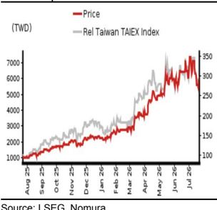
Research Analysts
Semiconductor
Aaron Jeng, CFA - NITB aaron.jeng@nomura.com +886(2) 21769962
Vivian Yang - NITB vivian.yang@nomura.com
+886(2) 21769970
Eric Chen, CFA - NITB
eric.chen@nomura.com +886(2) 21769965
Key data on MPI Corporation
Performance
| (%) | 1M | 3M | 12M | ||
|---|---|---|---|---|---|
| Absolute (TWD) | -6.6 | 24.4 | 474.2 | M cap (USDmn) | 18,184.5 |
| Absolute (USD) | -8.5 | 21 | 423.5 | Free float (%) | 75.9 |
| Rel to Taiwan TAIEX Index | -0.5 | 6 | 379.2 | 3-mth ADT (USDmn) | 219.7 |
Income statement (TWDmn)
| Year-end 31 Dec | FY24 | FY25 | FY26F | FY27F | FY28F |
|---|---|---|---|---|---|
| Revenue | 10,172 | 13,371 | 21,467 | 42,733 | 66,791 |
| Cost of goods sold | -4,611 | -5,943 | -8,935 | -16,974 | -25,769 |
| Gross profit | 5,561 | 7,428 | 12,532 | 25,759 | 41,022 |
| SG&A | -1,989 | -2,377 | -4,015 | -7,543 | -10,458 |
| Employee share expense | -1,089 | -1,276 | -1,726 | -2,991 | -3,409 |
| Operating profit | 2,483 | 3,775 | 6,791 | 15,225 | 27,155 |
| EBITDA | 3,039 | 4,566 | 7,851 | 16,302 | 28,264 |
| Depreciation | -474 | -655 | -898 | -954 | -1,018 |
| Amortisation | -83 | -136 | -162 | -123 | -91 |
| EBIT | 2,483 | 3,775 | 6,791 | 15,225 | 27,155 |
| Net interest expense | 9 | 4 | -4 | -12 | 82 |
| Associates & JCEs | |||||
| Other income | 303 | 66 | 472 | 362 | 381 |
| Earnings before tax | 2,795 | 3,844 | 7,259 | 15,574 | 27,618 |
| Income tax | -490 | -666 | -1,420 | -3,047 | -5,404 |
| Net profit after tax | 2,304 | 3,179 | 5,839 | 12,527 | 22,214 |
| Minority interests | 1 | 1 | 0 | 0 | 0 |
| Other items | -4 | -3 | 10 | 26 | 42 |
| Preferred dividends | |||||
| Normalised NPAT | 2,301 | 3,177 | 5,848 | 12,553 | 22,256 |
| Extraordinary items | |||||
| Reported NPAT | 2,301 | 3,177 | 5,848 | 12,553 | 22,256 |
| Dividends | -1,508 | -2,156 | -3,162 | -6,902 | -12,237 |
| Transfer to reserves | 794 | 1,021 | 2,686 | 5,651 | 10,019 |
| Valuations and ratios | |||||
| Reported P/E (x) | 245.7 | 179.1 | 100.5 | 46.8 | 26.4 |
| Normalised P/E (x) | 245.7 | 179.1 | 100.5 | 46.8 | 26.4 |
| FD normalised P/E (x) | 245.7 | 179.1 | 100.5 | 46.8 | 26.4 |
| Dividend yield (%) | 0.3 | 0.4 | 0.5 | 1.2 | 2.1 |
| Price/cashflow (x) | 201.7 | 160.5 | 449.0 | 84.7 | 32.7 |
| Price/book (x) | 60.8 | 38.7 | 31.0 | 20.5 | 13.1 |
| EV/EBITDA (x) | 192.9 | 128.1 | 75.1 | 36.0 | 20.4 |
| EV/EBIT (x) | 236.2 | 155.0 | 86.8 | 38.6 | 21.3 |
| Gross margin (%) | 54.7 | 55.6 | 58.4 | 60.3 | 61.4 |
| EBITDA margin (%) | 29.9 | 34.1 | 36.6 | 38.1 | 42.3 |
| EBIT margin (%) | 24.4 | 28.2 | 31.6 | 35.6 | 40.7 |
| Net margin (%) | 22.6 | 23.8 | 27.2 | 29.4 | 33.3 |
| Effective tax rate (%) | 17.5 | 17.3 | 19.6 | 19.6 | 19.6 |
| Dividend payout (%) | 65.5 | 67.9 | 54.1 | 55.0 | 55.0 |
| ROE (%) | - | 26.6 | 35.7 | 54.8 | 63.1 |
| ROA (pretax %) | - | 24.1 | 29.5 | 48.1 | 68.9 |
| Growth (%) | |||||
| Revenue | 31.5 | 60.5 | 99.1 | 56.3 | |
| EBITDA | 50.3 | 71.9 | 107.6 | 73.4 | |
| Normalised EPS | 37.1 | 78.2 | 114.6 | 77.3 | |
| Normalised FDEPS | 37.1 | 78.2 | 114.6 | 77.3 |
Source: Company data, Nomura estimates
Cashflow statement (TWDmn)
| Year-end 31 Dec | FY24 | FY25 | FY26F | FY27F | FY28F |
|---|---|---|---|---|---|
| EBITDA | 3,039 | 4,566 | 7,851 | 16,302 | 28,264 |
| Change in working capital | -1,235 | -682 | -5,806 | -6,686 | -5,371 |
| Other operating cashflow | 1,000 | -338 | -736 | -2,672 | -4,899 |
| Cashflow from operations | 2,804 | 3,546 | 1,309 | 6,944 | 17,994 |
| Capital expenditure | -1,229 | -3,881 | -2,690 | -1,709 | -1,670 |
| Free cashflow | 1,575 | -336 | -1,380 | 5,235 | 16,324 |
| Reduction in investments | -18 | -600 | -668 | 0 | 0 |
| Net acquisitions | |||||
| Dec in other LT assets | |||||
| Inc in other LT liabilities Adjustments | -97 | 406 | -14 | 0 | 0 |
| CF after investing acts | 1,461 | -530 | -2,063 | 5,235 | 16,324 |
| Cash dividends | -707 | -1,508 | -2,156 | -3,162 | -6,902 |
| Equity issue | 0 | -63 | 0 | 0 | 0 |
| Debt issue | 482 | 4,050 | 38 | 0 | 0 |
| Convertible debt issue | |||||
| Others | -125 | -208 | -24 | 0 | 0 |
| CF from financial acts | -350 | 2,272 | -2,142 | -3,162 | -6,902 |
| Net cashflow | 1,110 | 1,742 | -4,205 | 2,073 | 9,422 |
| Beginning cash | 2,585 | 3,695 | 5,437 | 1,233 | 3,306 |
| Ending cash | 3,695 | 5,437 | 1,233 | 3,306 | 12,728 |
| Ending net debt | -1,532 | -2,734 | 1,509 | -564 | -9,987 |
| Balance sheet (TWDmn) | |||||
| As at 31 Dec | FY24 | FY25 | FY26F | FY27F | FY28F |
| Cash & equivalents | 3,695 | 5,437 | 1,233 | 3,306 | 12,728 |
| Marketable securities | 0 | 0 | 0 | 0 | 0 |
| Accounts receivable | 2,050 | 2,411 | 4,519 | 7,706 | 7,753 |
| Inventories | 3,477 | 5,011 | 9,715 | 14,043 | 20,819 |
| Other current assets | 283 | 458 | 531 | 531 | 531 |
| Total current assets | 9,505 | 13,318 | 15,998 | 25,586 | 41,831 |
| LT investments Fixed assets | 336 | 702 | 1,293 | 1,293 12,268 | 1,293 12,920 |
| Goodwill | 6,074 | 9,867 | 11,513 | ||
| Other intangible assets | 318 | 581 | 474 | 351 | 260 |
| Other LT assets | 245 | -466 | -494 | -494 | -494 |
| Total assets | 16,479 | 24,003 | 28,784 | 39,004 | 55,810 |
| 858 | 881 | 881 | |||
| Short-term debt | 1,366 | 881 | 4,461 | ||
| Accounts payable | 766 | 1,342 | 2,180 | 3,009 | |
| Other current liabilities Total current liabilities | 4,050 | 4,862 | 5,102 8,163 | 5,102 8,992 | 5,102 10,444 |
| 5,673 | 7,569 | ||||
| Long-term debt | 1,305 | 1,337 | 1,861 | 1,861 | 1,861 |
| Convertible debt | |||||
| Other LT liabilities | 193 | 518 | 540 | 540 | 540 |
| Total liabilities | 7,172 | 9,424 | 10,563 | 11,392 | 12,844 |
| Minority interest | 4 | 0 | 0 | 0 | 0 |
| Preferred stock | 0 | 0 | 0 | 0 | 0 |
| Common stock | 2,687 | 6,145 | 6,145 | 6,145 | 6,145 |
| Retained earnings | 5,511 | 6,947 | 10,640 | 20,031 | 35,385 |
| Other equity and | |||||
| Proposed dividends reserves | 1,105 | 1,486 | 1,436 | 1,436 | 1,436 |
| Total shareholders' equity | 9,303 | 14,579 | 18,221 | 27,612 | 42,966 |
| Total equity & liabilities | 16,479 | 24,003 | 28,784 | 39,004 | 55,810 |
| Liquidity (x) | |||||
| Current ratio | 1.68 | 1.76 | 1.96 | 2.85 | 4.01 |
| Interest cover Leverage | - | - | 1,712.1 | 1,260.9 | - |
| Net debt/EBITDA (x) (%) | net cash | net cash | 0.19 8.3 | net cash net cash | net cash |
| Net debt/equity | net cash | net cash | net cash | ||
| 24.42 | |||||
| Per share | |||||
| Reported EPS (TWD) | 33.49 | 59.69 | 128.12 | 227.15 | |
| Norm EPS (TWD) (TWD) | 24.42 | 33.49 | 59.69 | 128.12 | 227.15 |
| FD norm EPS BVPS (TWD) | 24.42 98.72 | 33.49 154.84 | 59.69 193.53 | 128.12 293.27 | 227.15 456.35 |
| DPS (TWD) | 15.99 | 22.00 | 32.27 | 70.44 | 124.89 |
| Activity (days) | |||||
| Days receivable | 73.8 | 60.9 | 58.9 | 52.2 | 42.4 |
| Days inventory | 246.6 | 260.7 | 300.8 | 255.4 | 247.6 |
| Days payable | 60.8 | 64.7 | 71.9 | 55.8 | 53.1 |
| Cash cycle | 259.6 | 256.8 | 287.8 | 251.9 | 236.9 |
Source: Company data, Nomura estimates
Company profile
Established in 1995 in Hsinchu, MPI started its business with cantilever probe cards, and subsequently expanded into vertical probe cards (VPC), MEMS probe cards, LED/photonics test and sorting equipment, engineering probers and thermal systems.
Valuation Methodology
Our TP of TWD8,000 is based on 45x 2027-28F average EPS. 45x is at its high end of historical range. The benchmark is TAIEX.
Risks that may impede the achievement of the target price
Major downside risks to our TP include: 1) weaker demand in the AI/HPC market or slowdown of AI proliferation, 2) fierce competition in the test interface market and share loss, and 3) worse-than-expected progress of CPO.
ESG
MPI runs an ESG Committee chaired by the president, which sets short- to long-term sustainability targets and reports to the board at least annually. Environmental priorities cover GHG, water, waste, and hazardous substance management under group-wide carbon reduction plans, disclosed in a sustainability report published since 2023.
Insertion 2
Insertion 3
At the center of CPO testing flow
A key candidate of high-value-added CPO insertions
Silicon Photonics (Siph) / Co-Packaged Optics (CPO) is one of the rising trends in semiconductor manufacturing. We have detailed our understanding of testing flows in CPO testing in our Anchor Report and in Fig. 109 . Our understanding of CPO testing insertion is as follows: Insertion 1 is PIC and EIC single-sided wafer-level test; Insertion 2 is doublesided wafer-level test after hybrid bonding; Insertion 3 may include two optical engine (OE)level testing steps after singulation - before and after packaging (attach FAUs [fiber array units]/receptacle/ structural reinforcements), and Insertion 4 is the module-level test after the optical engine is mounted on the substrate. Silicon
Insertion 4
Silicon
Substrate
While final testing flows and vendor selection could vary by different customers, we expect MPI to leverage its expertise and experience in the PA/LED (Photonics Automation) and AST (Advanced Semiconductor Test) segments, leading to more opportunities to address Insertion 2 - where EPIC wafer is tested (double-sided), and part of Insertion 3 - focusing on die-level-testing, before packaging, given its competency in wafer probing. We believe MPI has commenced small volume Insertion 3 equipment shipments in 2H26, as industry players are still determining the testing flow and will have to carry out many trials before volume production. Insertion 2 is the most critical and complicated part in the process, in our view, and we believe many suppliers are now actively developing suitable equipment for the stage, and MPI also participates.
Our view on the CPO timeline now largely aligns with nVidia's (NVDA US, Not rated) product roadmap - for scale-out switch to ramp in 2H26F along with the Rubin platform (see 2026 GTC note ). However, given that there are many technical challenges for the brand-new architecture, we expect any large volume to come in 2027F and beyond, and the TAM will likely expand further after CPO penetrates into scale-up (likely in Feynman). However, many fabless companies beyond nVidia, such as Marvell (MRVL US, Not rated)/Broadcom (AVGO US, Not rated), as well as foundries such as GlobalFoundries (GFS US, Not rated) and Tower Semi (TSEM US, Not rated), are also developing their own CPO roadmap - not necessarily aligning with TSMC's (2330 TT, Buy) COUPE platform creating substantial future opportunities for supply chain vendors once CPO proliferates.
Fig. 109: CPO insertion flow
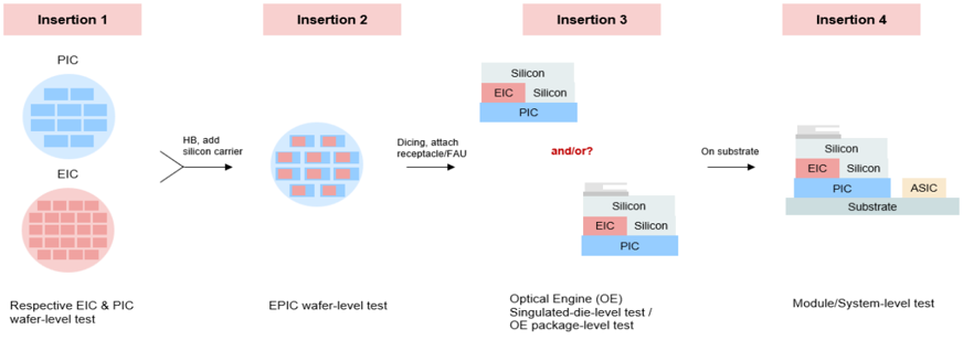
Note: This is a conceptual illustration, not specific to any company or project.
Source: Nomura research
Fig. 110: CPO insertion flow and potential suppliers
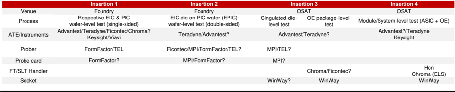
| Insertion 1 | Insertion 2 | Insertion 3 | Insertion 3 | Insertion 4 | |
|---|---|---|---|---|---|
| Venue | Foundry | Foundry | OSAT | OSAT | OSAT |
| Process | Respective EIC & PIC wafer-level test (single-sided) | EIC die on PIC wafer (EPIC) wafer-level test (double-sided) | Singulated-die- level test | OE package-level test | Module/System-level test (ASIC + OE) |
| ATE/Instruments | Advantest/Teradyne/Ficontec/Chroma? Keysight/Viavi | Teradyne/Advantest? | Advantest/Teradyne? | Advantest/Teradyne? | Advantest?/Teradyne Keysight |
| Prober | FormFactor/TEL | Ficontec/MPI/FormFactor/TEL? | MPI/TEL? | ||
| Probe card | FormFactor? | MPI/FormFactor? | MPI? | ||
| FT/SLT Handler | Chroma/Ficontec? | Hon Chroma (ELS) | |||
| Socket | WinWay? | WinWay | WinWay |
Source: Nomura research
ASIC
Unabated probe card demand across the board
Probe card to record 91% revenue CAGR over 2026-28F; MEMS's penetration continues to increase
MPI is one of the leading probe card vendors globally - it ranked No.4 in the total ownmake IC probe card market in 2025, according to Yole, mainly providing cantilever probe cards for display driver ICs (DDIC) and vertical probe cards for high-end logic products. We have described the technology trend of a probe card and requirements to migrate to MEMS-type (Micro-Electro-Mechanical Systems) probe cards in our Anchor Report, and fine pitch is one key factor for adoption of MEMS. While there is no precise boundary, conventionally manufactured probes cannot deliver the required positional accuracy after a certain level of pitch (we believe 50-70 µm; see Fig. 113: Typical pitch regimes and corresponding test interface solutions ). Currently, advanced smartphone application processor has a bump pitch of around 80 µm, and HPC/AI chips' pitch is around 100 µm, and hence, vertical probe cards are still widely adopted, though the trend is moving toward MEMS.
MPI is proactively expanding its MEMS capacity to catch up with testing requirements for AI chips, and to compete with overseas suppliers. Considering that MEMS pin's content value could be higher than cobra pins, we expect more projects migrating to MEMS probe card to fuel MPI's probe card segment. MPI is also building its own PCB fab and expects to enter the production stage in 2027E to shorten production lead times (mitigate supply chain bottlenecks), while the company will continue with its dual-source strategy of both in-house manufacturing and external procurement. We expect the probe card segment to show the strongest revenue growth over 2026-28F (91% CAGR), and MEMS penetration to rise continuously.
Probe card value content to surge along with higher testing requirements
Every dimension of advanced silicon is simultaneously raising the bar for probe cards and leading to higher content value
Larger die and package sizes expand the probe array's physical footprint, demanding tighter planarity control across a wider area, since the tolerance for total height deviation does not scale with size. Higher pin counts push arrays into the tens of thousands of probes, multiplying both the precision-manufacturing content and the routing burden on the PCB and space transformer beneath. We believe AI ASIC's pin count would rise from 20-25k to 30-40k+, after migration from cobra to MEMS. Higher current-carrying capacity (CCC) requirements (driven by kilowatt-class power delivery) force redesigned probe geometries with larger cross-sections and thermally robust materials, working directly against the simultaneous demand for fine pitch, where probes must shrink to serve sub-100 µm interfaces. High-speed signals (112G/224G SerDes) impose strict impedance and inductance budgets on contact design, while low contact force becomes mandatory as probes touch fragile low-k pads and micro-bumps that cannot tolerate conventional scrub. Furthermore, the wide temperature operation requires the entire card assembly to hold alignment and planarity across thermal expansion cycles. We believe all these stringent requirements are driving more sophisticated and expensive probe cards.
Advanced packaging's multiplier effect on probe cards
The chiplet architecture actually creates more probe card demand, as separated dies/tiles are integrated on one interposer, meaning that a single end-product no longer maps to a single probe card. The final module integrates multiple components from different wafers and process nodes (e.g., GPU/compute dies, I/O dies, HBM stacks, and a silicon interposer), and each demands its own dedicated probe card for wafer test. A highpin-count, high-current MEMS vertical card for the logic die; memory-class cards with repair flows for HBM; and specialized open/short test solutions for the interposer's fine micro-bumps and TSVs. Beyond the per-die dimension, the test flow adds cards by stage: separate hot and room-temperature insertions may require different thermalcompensation designs, and wafer-level burn-in (WLBI) uses full-wafer contactors built on an entirely different design philosophy from CP cards. Finally, the intermediate test at the CoW stage probes the reconstituted wafer after die attach, whose pad layout differs completely from native wafers and therefore mandates another freshly designed card. In total, a single CoWoS module can be supported by 3-5+ distinct probe card designs, spread across different suppliers and ecosystems. Every additional die in the package,
50,000
40,000
30,000
20,000
10,000
vve eoullale ayylessive expallolol piallo lui Melo Il 4uz0-<0r rich langes die malcalive, bourualles betweell dujacent lech blogles die tans ton zones whele solutions ovellap
Cantilever (peripheral pad)
140%
120%
and every additional assembly step, multiplies the variety and count of probe cards required. 80% 10,000
60%
8,000
wafer-level (probe card)
6,000
4,000
2,000
Fig. 112: MPI - Probe capacity expansion trend We estimate aggressive expansion plans for MEMS in 2026-28F
WLCSP
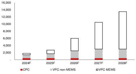
Note: Year-end capacity; kpm
Source: Company data, Nomura estimates
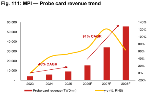
Source: Company data, Nomura estimates
Fig. 113: Typical pitch regimes and corresponding test interface solutions
Pitch ranges are indicative; boundaries between adjacent technologies are transition zones where solutions overlap
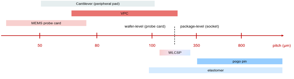
Note: This is a conceptual illustration, not specific to any company or project. Source: Nomura research
Overflowing pipeline of new projects
Dominant share in US ASIC vendors; packed pipeline of new projects
MPI is major supplier to key US ASIC providers as it specializes in high-speed and highfrequency probe cards, which are most suitable for networking products. Along with the AI boom, we believe these ASIC vendors take critical share of top-4 hyperscalers' ASICs projects, and thus MPI is one of the key beneficiaries under the trend. As probe card shipments usually commence before chip volume ramping (Fig. 114 ), we could already see MPI generating revenue from key ASICs projects starting from end 2025 to early 2026, preparing for those projects expected to ramp in 2H26.
Dynamics between ASICs and test interface suppliers
The decision-making process for test interface procurement is being redrawn in the AI era. In the traditional model, the chip designer largely dictated the choice of test interface vendor: the fabless company or IDM owned the test program and qualified the suppliers, and the rest of the chain followed. The AI chip era has fractured that simplicity. An AI accelerator now passes through the fabless/design service partner defining the test strategy, hyperscalers/end customers whose reliability requirements reach backward into the supply chain, and other supply chain partners may also provide opinions. The result is that no single party fully controls test interface selection. Yet, complexity also provides entry points, since a supplier locked out at the fabless level may still win the project through end customer or manufacturing partners. In addition, chiplet architecture creates demand for multiple probe card designs for a single project, and they could potentially be allocated to different probe card vendors, depending on each probe card's requirements. We believe the trend opens the door to suppliers with technology expertise such as MPI.
16,000
1ool Tlaruware lo
-12m olureu volure a uillp o mlaso viuuucllul!
Full range of products for the applications sufficient coverage solutions to IC markets
Not a bystander in key GPU leader's supply chain
production shipment
Along with MPI's in-house manufacturing capability and scale, as well as broad coverage of probes (Fig. 115 ), we believe the company stands in a favorable position to participate in different vendors' projects. Also, given the unprecedented CPU demand from Agentic AI, we believe MPI is enjoying some spillover orders from overseas leading probe card vendors. discussion R&D sample shipment Multimedia
Fig. 114: Timeline of testing equipment and interface preparation
Test hardware is shipped before a chip's mass production
COF / COG
Wire-Bond
Soldering Bumps
Cu-Pillar Bumps
COWOs
MPICORPORATION
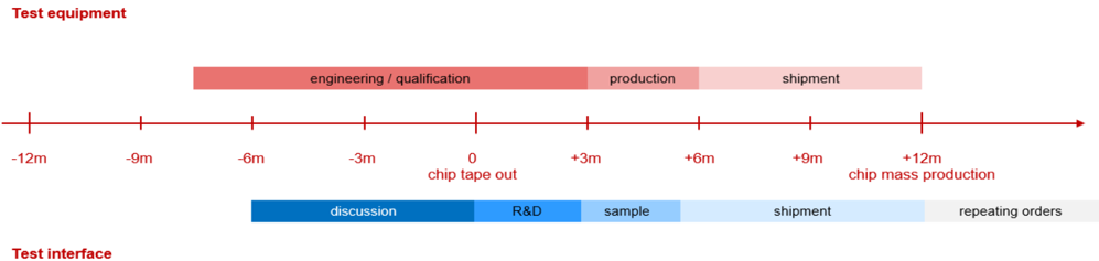
Note: This is a conceptual illustration, not specific to any company or project. Source: Nomura research
Fig. 115: MPI provides a broad range of probes
Different types of probes suit different applications and device pitch
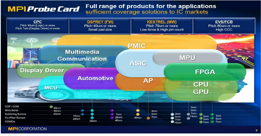
Source: Company data, Nomura research
MPU
FPGA
EVS/FCB
Pitch 80um or more
High CCC
+12m chip mass production
repeating orders
Steady growth from other business
Other than probe cards (which accounted for 70+% of total revenue in 1Q26), MPI still has revenue streams from its equipment business, spanning Photonics Automation (LED/PA; ~5% of total revenue), Advanced Semi Test (AST; 10-15% of total revenue), Thermal Test (TS; ~5% of total revenue). Since 2026, MPI has combines its PA (LED) and AST segments, partially because CPO actually utilizes both segments' technology. Among all the equipment segments, we believe PA/AST will show obvious growth once CPO ramps.
Photonics Automation (LED/PA; ~5% of total revenue): mainly serves wafer probing stages, for LEDs and optoelectronic devices, including testers, material handlers, and inspection systems, serving applications such as LEDs, photodetectors, and lasers. The latest technologies such as VCSEL (Vertical-Cavity Surface-Emitting Laser) and Micro LED are now major revenue contributors within the segment.
Advanced Semi Test (AST; 10-15% of total revenue): this segment is more like an extension of the probe card business, in which MPI supplies some testing equipment (probing systems) to IC design houses/foundries for the purpose of detecting failures of sample wafers inside their fabs (not in OSATs). Its silicon photonics test solutions feature flexible-configuration high-precision fiber alignment (single fibers or fiber arrays with one or two positioners), safety mechanisms including fiber-to-wafer distance monitoring and collision avoidance, a broad test temperature range from -50°C to 200°C, and a compact system design integrating silicon photonics control instruments, paired with SENTIO software. The company has also signed an MoU with Lightium AG (unlisted) and Axiomatic_AI (unlisted) to jointly develop an AI-driven Intelligent, Autonomous, and Integrated Test Solution (IAITS) for PIC devices (press release ).
Thermal Test (TS; ~5% of total revenue): MPI supplies thermal systems for chips (after packaging) that will be used in extreme temperature environments, such as autos, satellites, fiber optics, sensing and telecommunication-related (5G/RF) applications. MPI's thermal system can cover temperate range from -100°C to 300°C, and we may also see some growth for the segment due to the rising TDP (thermal design power) of AI/HPC chips, with MPI having a competitive advantage in power saving.
The rest of business: MPI acquired Celadon Systems in 2021. Celadon is a global leader in engineering probe cards for parametric test, wafer-level reliability (WLR), characterization, cryogenic, and high-power applications, known for ultra-highperformance cards that thrive in extreme temperatures. MPI stated the acquisition would strengthen its leading position in test and enable more comprehensive products and services in which Celadon's cards are integrated into MPI's automated probe systems (synergy with AST segment), making high-density, multi-site, high-temperature WLR testing easy and versatile. Besides, MPI has low-single-digit revenue contribution from its overseas subsidiaries for distribution services and after-sales support.
8,000
1,000
7,000
800
6,000
5,000
600
4,000
400
3,000
2,000
200
1,000
vIll
Share price recap
1,600,000
2,000,000
1,800,000
1,400,000
1,600,000
1,200,000
1,400,000
400,000
MPI's share price was relatively stable before 2023 (TWD79 at the beginning of 2020, and TWD113 at end-2022, benefiting from remote working [WFH] demand during COVID but undergoing an inventory correction afterwards). Since then, due to the AI boom (from end-2022), MPI's share price has risen on the AI trend (TWD118 at the beginning of 2023, reaching the TWD6,000-7,000 level in 2Q26), up 60x since 2023 vs TAIEX up 200%+. 1,000,000 600,000 Macro: 1,200,000 800,000 600,000
Along with the company's capacity expansion plans and major clients' project ramp-ups (both graphics and ASICs), MPI's revenue scale also expanded from the TWD500-600mn level in 2023 to TWD1,200-1,400mn in 2025, and exceeded the TWD1,800mn level in May-Jun 2026 (on a monthly basis). Fundamental strength (as shown in monthly revenue) remains one key factor behind its share price uptrend. Despite some correction from time to time, either due to (likely) phased profit taking or macro headwinds, the stock has remained on an upward trajectory over the past few years. 200,000 400,000 200,000
Further, from late 2025 to early 2026, there was increasing market discussion about optical communications/CPO, triggering a share price uptrend, as we believe MPI is participating in the CPO testing process (see At the center of CPO testing flow ). The successful launch of Gemini 3 in Nov-25 jointly ignited the large rally, in our view. Since 2Q26, there has been increasing visibility on MPI's probe card business, and we see continuous upward revisions to capacity expansion plans and capex. We also expect the company to have better pricing power, and some share gain opportunities amid a supply-constrained environment, all leading to share price momentum.
Fig. 116: MPI share price events vs monthly sales, 2023-24
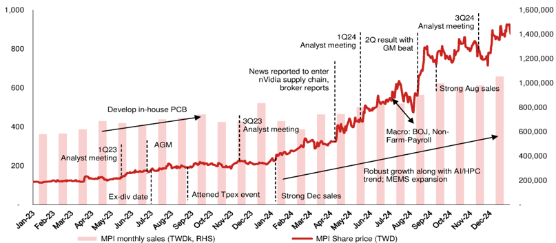
Source: TEJ, company data, Nomura research
Fig. 117: MPI's share price event chart vs monthly sales, 2025-26YTD
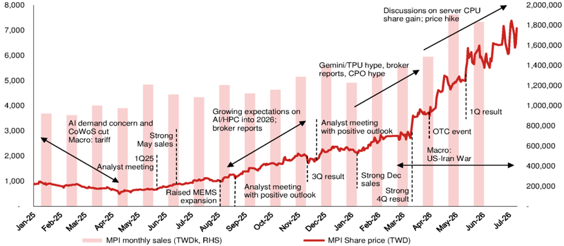
Source: TEJ, company data, Nomura research
Discussions on server CPU
share gain; price hike
3Q24|
Analyst meeting
1024 ÷ 20 result with
Analyst meeting
GM beat
Financial analysis and forecasts
76% revenue CAGR over 2026-28F; probe card business to lead growth
We believe MPI has a broad customer base covering ASIC vendors/GPU vendors, for both AI and non-AI applications, and that its in-house manufacturing capability (especially, MEMS probes) will support the company's growth along with stringent requirements for probe cards and the necessity of using MEMS probes. We model a 76% total revenue CAGR over 2026-28F, vs 28% in 2023-25 (Fig. 119 ). Within the segments, we expect the probe card segment to lead the revenue momentum alongside CPO equipment.
Gross margin solid; increasing MEMS penetration to fuel profitability
We detailed the difficulty for probe card design in the above section to cope with advanced chip spec such as larger package size, fine-pitch, and to satisfy higher speed and frequency requirements. Along with complex design, we believe pricing will reflect the company's value. Besides, we also expect the migration to MEMS will result in ASP and margin upside. We expect MPI's GM to improve from 55%+ in 2025 to 61% in 2028F, and coupled with well-controlled expenses, we model EPS to surge from TWD33 in 2025 to TWD227 in 2028F (Fig. 122 ).
Fig. 118: MPI - key financial figures
| 2023 | 2024 | 2025 | 2026F | 2027F | 2028F | 2026-28F CAGR | 2023-25 CAGR | |
|---|---|---|---|---|---|---|---|---|
| Key financial numbers (TWD mn) | Key financial numbers (TWD mn) | Key financial numbers (TWD mn) | Key financial numbers (TWD mn) | Key financial numbers (TWD mn) | Key financial numbers (TWD mn) | Key financial numbers (TWD mn) | Key financial numbers (TWD mn) | Key financial numbers (TWD mn) |
| Net revenue | 8,147 | 10,172 | 13,371 | 21,467 | 42,733 | 66,791 | 76% | 28% |
| y-y (%) | 10% | 25% | 31% | 61% | 99% | 56% | ||
| Gross profit | 3,897 | 5,561 | 7,428 | 12,532 | 25,759 | 41,022 | 81% | 38% |
| y-y (%) | 14% | 43% | 34% | 69% | 106% | 59% | ||
| GM (%) | 48% | 55% | 56% | 58% | 60% | 61% | ||
| Operating profit | 1,471 | 2,483 | 3,775 | 6,791 | 15,225 | 27,155 | 100% | 60% |
| y-y (%) | 18% | 69% | 52% | 80% | 124% | 78% | ||
| OpM (%) | 18% | 24% | 28% | 32% | 36% | 41% | ||
| Net profit | 1,312 | 2,301 | 3,177 | 5,848 | 12,553 | 22,256 | 95% | 56% |
| y-y (%) | 8% | 75% | 38% | 84% | 115% | 77% | ||
| EPS (TWD) | 13.92 | 24.42 | 33.49 | 59.69 | 128.12 | 227.15 | 95% | 55% |
| y-y (%) | 8% | 75% | 37% | 78% | 115% | 77% | ||
| Revenue mix (TWD mn) | Revenue mix (TWD mn) | Revenue mix (TWD mn) | Revenue mix (TWD mn) | Revenue mix (TWD mn) | Revenue mix (TWD mn) | Revenue mix (TWD mn) | Revenue mix (TWD mn) | Revenue mix (TWD mn) |
| Probe card | 4,125 | 5,930 | 9,069 | 15,352 | 34,067 | 55,735 | 91% | 48% |
| PA/AST | 2,220 | 2,283 | 2,006 | 2,144 | 4,272 | 6,409 | 73% | -5% |
| Thermal Test | 399 | 508 | 552 | 652 | 736 | 778 | 9% | 18% |
| Others | 1,402 | 1,452 | 1,744 | 3,319 | 3,658 | 3,869 | 8% | 12% |
| Total | 8,147 | 10,172 | 13,371 | 21,467 | 42,733 | 66,791 | 76% | 28% |
| Revenue mix (%) | Revenue mix (%) | Revenue mix (%) | Revenue mix (%) | Revenue mix (%) | Revenue mix (%) | Revenue mix (%) | Revenue mix (%) | Revenue mix (%) |
| Probe card | 51% | 58% | 68% | 72% | 80% | 83% | ||
| PA/AST | 27% | 22% | 15% | 10% | 10% | 10% | ||
| Thermal Test | 5% | 5% | 4% | 3% | 2% | 1% | ||
| Others | 17% | 14% | 13% | 15% | 9% | 6% | ||
| Total | 100% | 100% | 100% | 100% | 100% | 100% |
Source: Company data, Nomura estimates
70,000
25,000
60,000
60,000
20,000
50,000
50,000
40,000
40,000
15,000
30,000
30,000
10,000
20,000
20,000
5,000
10,000
10,000
-
50%
120%
40%
250
45,000
100%
90%
40,000
200
35,000
80%
30,000
25,000
20,000
15,000
10,000
5,000
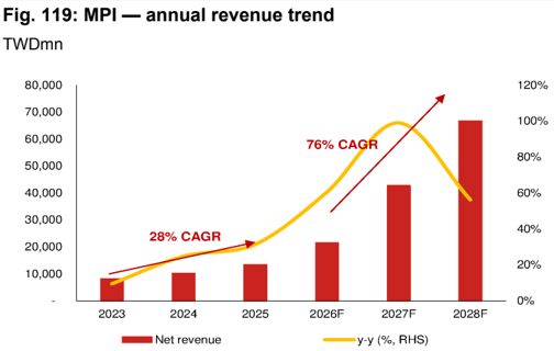
Source: Company data, Nomura estimates
Fig. 121: MPI - annual operating profit trend
TWDmn
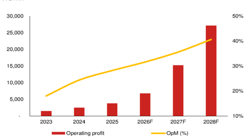
Source: Company data, Nomura estimates
Fig. 123: MPI's annual product mix
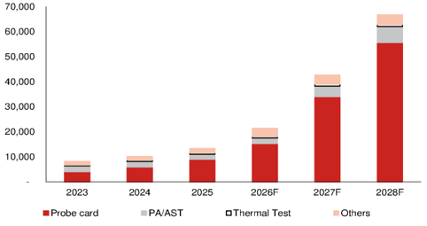
Source: Company data, Nomura estimates
120%
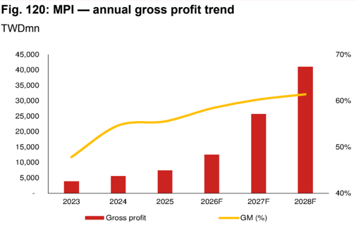
Source: Company data, Nomura estimates
Fig. 122: MPI - annual EPS trend
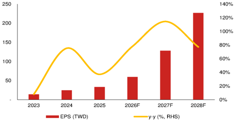
Source: Company data, Nomura estimates
Fig. 124: MPI's annual product mix
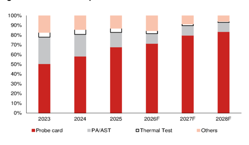
Source: Company data, Nomura estimates
Fig. 125: MPI P&L
| (TWD mn) | 1Q25 | 2Q25 | 3Q25 | 4Q25 | 1Q26 | 2Q26F | 3Q26F | 4Q26F | 1Q27F | 2Q27F | 3Q27F | 4Q27F | 2025 | 2026F | 2027F | 2028F |
|---|---|---|---|---|---|---|---|---|---|---|---|---|---|---|---|---|
| Net revenue | 2,829 | 3,293 | 3,414 | 3,836 | 3,933 | 5,226 | 5,662 | 6,646 | 7,987 | 9,709 | 12,194 | 12,843 | 13,371 | 21,467 | 42,733 | 66,791 |
| Gross profit | 1,623 | 1,919 | 1,822 | 2,063 | 2,338 | 2,968 | 3,306 | 3,921 | 4,738 | 5,814 | 7,379 | 7,828 | 7,428 | 12,532 | 25,759 | 41,022 |
| - OPEX | (783) | (840) | (927) | (1,104) | (1,065) | (1,385) | (1,511) | (1,779) | (1,964) | (2,392) | (3,009) | (3,169) | (3,653) | (5,741) | (10,534) | (13,867) |
| Operating profit | 840 | 1,079 | 896 | 959 | 1,273 | 1,583 | 1,795 | 2,141 | 2,774 | 3,422 | 4,370 | 4,659 | 3,775 | 6,791 | 15,225 | 27,155 |
| Net profit | 724 | 628 | 877 | 948 | 1,227 | 1,287 | 1,529 | 1,805 | 2,302 | 2,824 | 3,603 | 3,824 | 3,177 | 5,848 | 12,553 | 22,256 |
| EPS (TWD) | 7.68 | 6.67 | 9.30 | 9.99 | 12.53 | 13.13 | 15.60 | 18.42 | 23.50 | 28.82 | 36.77 | 39.03 | 33.49 | 59.69 | 128.12 | 227.15 |
| Profitability | 1Q25 | 2Q25 | 3Q25 | 4Q25 | 1Q26 | 2Q26F | 3Q26F | 4Q26F | 1Q27F | 2Q27F | 3Q27F | 4Q27F | 2025 | 2026F | 2027F | 2028F |
| Gross margin | 57.4% | 58.3% | 53.4% | 53.8% | 59.4% | 56.8% | 58.4% | 59.0% | 59.3% | 59.9% | 60.5% | 60.9% | 55.6% | 58.4% | 60.3% | 61.4% |
| - OPEX ratio | (27.7%) | (25.5%) | (27.1%) | (28.8%) | (27.1%) | (26.5%) | (26.7%) | (26.8%) | (24.6%) | (24.6%) | (24.7%) | (24.7%) | (27.3%) | (26.7%) | (24.7%) | (20.8%) |
| Operating margin | 29.7% | 32.8% | 26.2% | 25.0% | 32.4% | 30.3% | 31.7% | 32.2% | 34.7% | 35.2% | 35.8% | 36.3% | 28.2% | 31.6% | 35.6% | 40.7% |
| Net margin | 25.6% | 19.1% | 25.7% | 24.7% | 31.2% | 24.6% | 27.0% | 27.2% | 28.8% | 29.1% | 29.5% | 29.8% | 23.8% | 27.2% | 29.4% | 33.3% |
| Q-Q | 1Q25 | 2Q25 | 3Q25 | 4Q25 | 1Q26 | 2Q26F | 3Q26F | 4Q26F | 1Q27F | 2Q27F | 3Q27F | 4Q27F | 2025 | 2026F | 2027F | 2028F |
| Net revenue | (5.8%) | 16.4% | 3.7% | 12.4% | 2.5% | 32.9% | 8.3% | 17.4% | 20.2% | 21.6% | 25.6% | 5.3% | ||||
| Gross profit | (3.8%) | 18.2% | (5.0%) | 13.2% | 13.3% | 26.9% | 11.4% | 18.6% | 20.9% | 22.7% | 26.9% | 6.1% | ||||
| - OPEX | (16.2%) | 7.3% | 10.3% | 19.1% | (3.5%) | 30.1% | 9.1% | 17.7% | 10.4% | 21.8% | 25.8% | 5.3% | ||||
| Operating profit | 11.6% | 28.4% | (17.0%) | 7.1% | 32.7% | 24.3% | 13.4% | 19.3% | 29.5% | 23.4% | 27.7% | 6.6% | ||||
| Net profit | 1.2% | (13.2%) | 39.5% | 8.1% | 29.5% | 4.8% | 18.8% | 18.1% | 27.5% | 22.6% | 27.6% | 6.1% | ||||
| Y-Y | 1Q25 | 2Q25 | 3Q25 | 4Q25 | 1Q26 | 2Q26F | 3Q26F | 4Q26F | 1Q27F | 2Q27F | 3Q27F | 4Q27F | 2025 | 2026F | 2027F | 2028F |
| Net revenue | 38.2% | 37.6% | 25.1% | 27.7% | 39.0% | 58.7% | 65.9% | 73.2% | 103.1% | 85.8% | 115.4% | 93.3% | 31.5% | 60.5% | 99.1% | 56.3% |
| Gross profit | 58.2% | 47.6% | 17.8% | 22.2% | 44.0% | 54.6% | 81.4% | 90.1% | 102.7% | 95.9% | 123.2% | 99.7% | 33.6% | 68.7% | 105.5% | 59.3% |
| - OPEX | 22.5% | 19.6% | 15.5% | 18.1% | 36.0% | 64.9% | 63.1% | 61.2% | 84.4% | 72.7% | 99.1% | 78.1% | 18.7% | 57.1% | 83.5% | 31.6% |
| Operating profit | 117.3% | 80.6% | 20.2% | 27.4% | 51.5% | 46.7% | 100.3% | 123.2% | 117.9% | 116.2% | 143.5% | 117.6% | 52.0% | 79.9% | 124.2% | 78.4% |
| Net profit | 83.8% | 15.8% | 34.9% | 32.5% | 69.6% | 104.8% | 74.4% | 90.5% | 87.6% | 119.4% | 135.7% | 111.8% | 38.0% | 84.1% | 114.6% | 77.3% |
Source: Company data, Nomura estimates
Fig. 126: Nomura forecasts vs Bloomberg consensus estimates for 2026-28
| 2026F | 2026F | 2026F | 2027F | 2027F | 2027F | 2028F | 2028F | 2028F | |
|---|---|---|---|---|---|---|---|---|---|
| (TWD mn) | NMR | BBG | Diff (%) | NMR | BBG | Diff (%) | NMR | BBG | Diff (%) |
| Net sales | 21,467 | 23,191 | (7.4) | 42,733 | 46,202 | (7.5) | 66,791 | 72,018 | (7.3) |
| Gross profit | 12,532 | 14,123 | (11.3) | 25,759 | 28,969 | (11.1) | 41,022 | 45,731 | (10.3) |
| Operating profit | 6,791 | 7,986 | (15.0) | 15,225 | 17,556 | (13.3) | 27,155 | 29,113 | (6.7) |
| Net profit | 5,848 | 6,772 | (13.6) | 12,553 | 14,733 | (14.8) | 22,256 | 24,329 | (8.5) |
| EPS (TWD) | 59.69 | 64.95 | (8.1) | 128.12 | 124.02 | 3.3 | 227.15 | 257.50 | (11.8) |
| Margin | NMR | BBG | Diff (%) | NMR | BBG | Diff (%) | NMR | BBG | Diff (%) |
| Gross margin (%) | 58.4 | 60.9 | (2.5) | 60.3 | 62.7 | (2.4) | 61.4 | 63.5 | (2.1) |
| Operating margin (%) | 31.6 | 34.4 | (2.8) | 35.6 | 38.0 | (2.4) | 40.7 | 40.4 | 0.2 |
| Net margin (%) | 27.2 | 29.2 | (2.0) | 29.4 | 31.9 | (2.5) | 33.3 | 33.8 | (0.5) |
Source: Company data, Bloomberg Finance L.P., Nomura estimates
90
300
80
250
70
60
50
200
40
150
30
20
100
10
50
0
Jul-23
0
35
30
8,000
7,000
Valuation methodology and risks
Our TP of TWD8,000 is based on 45x 2027-28F average EPS. 45x is at a high end of its historical range (Fig. 127 ). MPI's historical trading range was15-30x in 2H23 to 1H25, before surging to as high as 80x in May 2026. Considering 76%/95% revenue/EPS CAGRs over 2026-28F (vs 28%/55% over 2023-25), we think a multiple slightly geared to the upper end is justified, given its in-house MEMS probe fabrication capability, less concentration risks due to a broad customer base, and key role in CPO testing, not to mention a P/E peak of 80x+ owing to the hype surrounding AI.
Risks to our call
- 2025E EPS
2026E EPS
Major downside risks to MPI include: 1) weaker demand in the AI/HPC market or a slowdown of AI proliferation; 2) fierce competition in the test interface market and share loss; and 3) worse-than-expected CPO progress.
Fig. 127: MPI's consensus 1BF P/E
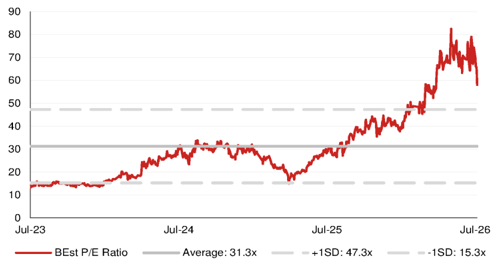
Source: Bloomberg Finance L.P., Nomura research
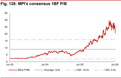
Source: Bloomberg Finance L.P., Nomura research
Fig. 129: MPI's share price vs Bloomberg consensus EPS estimate revisions
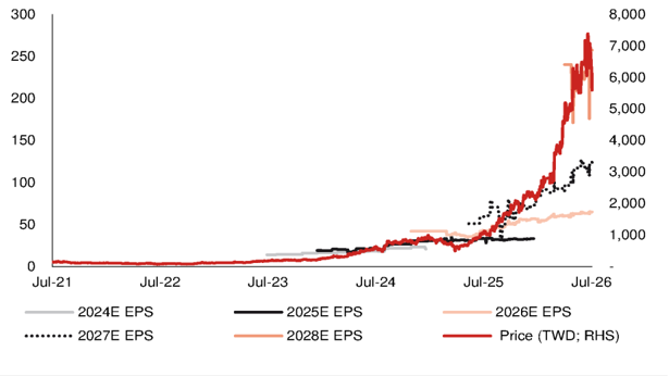
Source: Bloomberg Finance L.P., Nomura research
Jul-25
+1SD: 16.0x
Jul-26
-
- 1SD: 2.0x
40
30
20
10
0
Jan-21
Company profile
8,000
7,000
6,000
5,000
Established in 1995 in Hsinchu, MPI started its business with cantilever probe cards, and subsequently expanded into vertical probe cards (VPC), MEMS probe cards, LED/photonics test and sorting equipment, engineering probers and thermal systems through some M&A activities. MPI was officially listed on the TPEx in 2003, the first probe card company listed in Taiwan. Currently, its major business operations comprise Probe Card, Photonics Automation (PA)/Advanced Semi Test (AST), and Thermal Test divisions.
MPI designs and manufactures probe cards in-house, and can cover broad-based products including logic IC, RF, power/analog IC, CIS, and compound semiconductor/LED devices; its VPC and MEMS probe cards address AI/HPC wafer sort demand. For capacity allocation, manufacturing is mainly based in Hsinchu (MPI further announced that it would purchase land in Hukou in Apr-26), with ongoing capacity expansion for advanced probe cards. By product, probe cards accounted for 71% of the company's 1Q26 revenue, equipment was at 27%, and others at ~2%.
Fig. 130: MPI board of directors
| Title | Name | Term (years) | Shareholding (%) | Experience |
|---|---|---|---|---|
| Director | Green, Chang-Lin* | 3 | 1.9 | Electronics Research & Service Organization, Industrial Technology Research Institute |
| Director | Steve Chen* | 3 | 0.24 | Material and Chemical Research Laboratories, Industrial Technology Research Institute |
| Director | Tsai, Chang-Shou | 3 | 0.02 | Bureau of Accounting & Statistics, Provincial Government of Taiwan |
| Director | Scott Kuo* | 3 | 0.4 | Mechanical and Systems Research Laboratories, Industrial Technology Research Institute |
| Director | Li, Tu-Cheng | 3 | 0.42 | Chain-Logic International Corp. |
| Director | Liu, Fang-Sheng | 3 | 0.25 | Taipei City Hospital |
| Independent Director | Hsu, Mei-Fang | 3 | 0.13 | Baker Tilly Clock & CO |
| Independent Director | Kao, Chin-Cheng | 3 | 0.16 | Hui Lin Law Office |
| Independent Director | Liao, Da-Ying | 3 | 0 | Professor, Department of Law, National Chung Hsing University |
Note: *Representative of MPI Investment Co., Ltd. Data as of Apr 2026. Source: Company data, TEJ, Nomura research
Fig. 131: MPI's share price vs FINI holdings
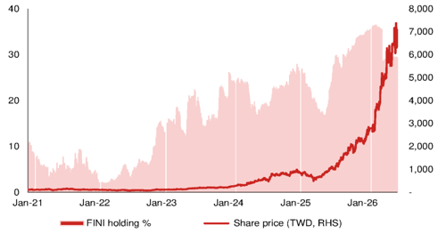
Source: TEJ, Nomura research
Fig. 132: MPI's top 10 shareholders
| Top 10 shareholders | % |
|---|---|
| MPI Investment Co., Ltd. | 8.51 |
| Labor pension fund under the new system | 8.49 |
| Allianz Global Investors Taiwan Technology Fund | 3.67 |
| Labor pension fund under the old system | 2.57 |
| Allianz Global Investors Taiwan Fund | 2.03 |
| Public Service Pension Fund | 1.98 |
| Citibank manages investment accounts at the Norwegian Central Bank | 1.68 |
| MPI Corporation's employee stock ownership trust property account in custody of Bank Sinopac | 1.65 |
| Standard Chartered Bank (custodian for Mizuho Securities Co., Ltd.) | 1.6 |
| Chang Hwa Commercial Bank, Ltd., is entrusted with the custody of the segregated account for the Uni-President Taiwan Growth Active ETF securities investment trust fund | 1.52 |
Note: Data as of 30 Apr-26
Source: Company data, Nomura research
Relative performance chart
EQUITY: OSAT
Price
(TWD)
10000
7500-
5000-
2500-
-
• 600
-
500
-
400|
-300
WinWay Technology 6515.TW 6515 TT
EQUITY: OSAT
Churra. I CEC Namura
Attractive valuation; initiate coverage at Buy
Ties with key AI chips to drive growth in probe card and socket businesses; improving risk-reward
Initiate coverage with a Buy rating and a TP of TWD8,315, implying 28% upside
We initiate coverage of WinWay with a Buy rating along with our Anchor Report. Our positive outlook for the company is premised on: 1) strong revenue growth prospects for its probe card segment, driven by AI, high-end graphics and networking products; 2) several upcoming new projects in the socket business, with WinWay enjoying a dominant share within leading GPU vendors, alongside share gains in the system-level-test (SLT) business; the upcoming TPU project likely to augment growth as well; 3) more testing insertions such as burn-in (BI) and SLT being added to the latest AI/HPC chips, and new testing processes such as functional burn-in being under consideration; 4) higher product value content led by requriements to address high pin count, larger package size, higher speed/frequency, and heat density, etc (Fig. 133 ); 5) WinWay's innovative solutions such as HyperSocket potentially taking off in 2028F (Fig. 137 ); and 6) WinWay engaging in high-profile CPO testing insertions, with opportunities for Insertion 3 and Insertion 4 (Fig. 141 Fig. 145 ), in our view. We expect revenues from the probe card and coaxial socket segments (already accounted for a combined 70% of total revenue in 1Q26) to record 67% and 86% CAGRs over 2026-28F, respectively. In terms of new business, we assume HyperSocket would account for ~5% of total revenue in 2028F (Fig. 137 ). Many of the developments discussed here are still at a nascent stage, but their directions are clear, i.e. most are anchored to structural forces and are difficult to reverse, in our view. Our TP of TWD8,315 is based on 32x 2027-28F average EPS. The 32x target multiple is in the middle of its historical trading range. Key risks include: 1) weaker demand in the AI/HPC market or a slowdown of AI proliferation, 2) fierce competition in the test interface market and share loss, and 3) worse-than-expected profitability.
Near-term share price weakness could provide attractive entry opportunity
WinWay's share price has corrected by 27% since July (vs. TAIEX down 5%), as rising macro risks and overall sentiment on AI has taken a slight turn amid concerns about New York's moratorium on data center development and Meta's (META US, Not rated) initiatives around Meta Compute . Its share price also reacted to company-specific issues, in our view, after the release of June earnings. We estimate 2QFY26F GM at 39.7%, considering the preliminary June results. While more clarity will emerge after its 2Q26 earnings release, an increase in revenue contribution from MEMS probe cards, as well as unfavorable product mix (more consumer electronics) are potential drivers for the likely narrowed 2Q26F GM. We expect the impact to be temporary, and GM to gradually trend up in 2H26F. We see short-term share price weakness as buying opportunities.
| Year-end 31 Dec Currency (TWD) | FY25 Actual | Old | FY26F New | Old | FY27F New | Old | FY28F New |
|---|---|---|---|---|---|---|---|
| Revenue (mn) | 7,857 | 0 | 14,458 | 0 | 24,959 | 0 | 41,219 |
| Reported net profit (mn) | 1,673 | 0 | 3,157 | 0 | 6,641 | 0 | 11,935 |
| Normalised net profit (mn) | 1,673 | 0 | 3,157 | 0 | 6,641 | 0 | 11,935 |
| FD normalised EPS | 46.93 | 88.32 | 185.76 | 333.86 | |||
| FD norm. EPS growth (%) | 36.8 | 88.2 | 110.3 | 79.7 | |||
| FD normalised P/E (x) | 138.5 | - | 73.6 | - | 35.0 | - | 19.5 |
| EV/EBITDA (x) | 100.6 | - | 59.0 | - | 27.6 | - | 15.2 |
| Price/book (x) | 36.3 | - | 32.7 | - | 20.6 | - | 12.8 |
| Dividend yield (%) | 0.8 | - | 1.0 | - | 2.2 | - | 3.9 |
| ROE (%) | 27.9 | 46.4 | 71.6 | 80.4 | |||
| Net debt/equity (%) | net cash | 9.5 | 20.8 | net cash |
Source: Company data, Nomura estimates jul
Global Markets Research 24 July 2026
| Rating Starts at | Buy |
|---|---|
| Target price Starts at | TWD 8,315.00 |
| Closing price 22 July 2026 | TWD 6,500.00 |
| Implied upside | +27.9% |
| Market Cap (USD mn) | 7,245.7 |
| ADT (USD mn) | 117.4 |
Relative performance chart
Source: LSEG, Nomura
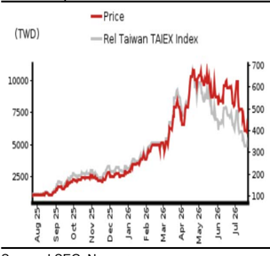
Research Analysts
Semiconductor
Vivian Yang - NITB vivian.yang@nomura.com +886(2) 21769970
Aaron Jeng, CFA - NITB
aaron.jeng@nomura.com +886(2) 21769962
Eric Chen, CFA - NITB
eric.chen@nomura.com +886(2) 21769965
Key data on WinWay Technology
Performance
| (%) | 1M | 3M | 12M | ||
|---|---|---|---|---|---|
| Absolute (TWD) | -31.3 | -39.4 | 550 | M cap (USDmn) | 7,245.7 |
| Absolute (USD) | -32.7 | -41.1 | 492.7 | Free float (%) | 74.9 |
| Rel to Taiwan TAIEX Index | -25.2 | -57.8 | 455 | 3-mth ADT (USDmn) | 117.4 |
Income statement (TWDmn)
| Year-end 31 Dec | FY24 | FY25 | FY26F | FY27F | FY28F |
|---|---|---|---|---|---|
| Revenue | 5,798 | 7,857 | 14,458 | 24,959 | 41,219 |
| Cost of goods sold | -3,265 | -4,301 | -8,533 | -14,083 | -22,809 |
| Gross profit | 2,534 | 3,556 | 5,925 | 10,876 | 18,409 |
| SG&A | -1,165 | -1,487 | -2,224 | -2,774 | -3,710 |
| Employee share expense | |||||
| Operating profit | 1,368 | 2,070 | 3,700 | 8,101 | 14,700 |
| EBITDA | 1,577 | 2,303 | 3,983 | 8,588 | 15,387 |
| Depreciation | -222 | -245 | -294 | -495 | -694 |
| Amortisation | 13 | 12 | 12 | 9 | 6 |
| EBIT | 1,368 | 2,070 | 3,700 | 8,101 | 14,700 |
| Net interest expense | 9 | 44 | 71 | 55 | 79 |
| Associates & JCEs | |||||
| Other income | 58 | -52 | 179 | 153 | 154 |
| Earnings before tax | 1,435 | 2,061 | 3,950 | 8,309 | 14,933 |
| Income tax | -249 | -388 | -793 | -1,668 | -2,998 |
| Net profit after tax | 1,186 | 1,673 | 3,157 | 6,641 | 11,935 |
| Minority interests | 0 | 0 | 0 | 0 | |
| Other items | |||||
| Preferred dividends | |||||
| Normalised NPAT | 1,186 | 1,673 | 3,157 | 6,641 | 11,935 |
| Extraordinary items | |||||
| Reported NPAT | 1,186 | 1,673 | 3,157 | 6,641 | 11,935 |
| Dividends | -890 | -1,787 | -2,422 | -5,034 | -9,005 |
| Transfer to reserves | 296 | -115 | 736 | 1,607 | 2,930 |
| Valuations and ratios | |||||
| Reported P/E (x) | 189.5 | 138.5 | 73.6 | 35.0 | 19.5 |
| Normalised P/E (x) | 189.5 | 138.5 | 73.6 | 35.0 | 19.5 |
| FD normalised P/E (x) | 189.5 | 138.5 | 73.6 | 35.0 | 19.5 |
| Dividend yield (%) | 0.4 | 0.8 | 1.0 | 2.2 | 3.9 |
| Price/cashflow (x) | 214.2 | 128.5 | 126.6 | 56.3 | 22.0 |
| Price/book (x) | 41.1 | 36.3 | 32.7 | 20.6 | 12.8 |
| EV/EBITDA (x) | 147.9 | 100.6 | 59.0 | 27.6 | 15.2 |
| EV/EBIT (x) | 170.5 | 111.9 | 63.5 | 29.2 | 15.9 |
| Gross margin (%) | 43.7 | 45.3 | 41.0 | 43.6 | 44.7 |
| EBITDA margin (%) | 27.2 | 29.3 | 27.5 | 34.4 | 37.3 |
| EBIT margin (%) | 23.6 | 26.3 | 25.6 | 32.5 | 35.7 |
| Net margin (%) | 20.5 | 21.3 | 21.8 | 26.6 | 29.0 |
| Effective tax rate (%) | 17.3 | 18.8 | 20.1 | 20.1 | 20.1 |
| Dividend payout (%) | 75.1 | 106.8 | 76.7 | 75.8 | 75.4 |
| ROE (%) | 26.3 | 27.9 | 46.4 | 71.6 | 80.4 |
| ROA (pretax %) | 25.6 | 32.1 | 37.4 | 47.8 | 64.3 |
| Growth (%) | |||||
| Revenue | 57.5 | 35.5 | 84.0 | 72.6 | 65.1 |
| EBITDA | 139.1 | 46.0 | 72.9 | 115.6 | 79.2 |
| Normalised EPS | 153.7 | 36.8 | 88.2 | 110.3 | 79.7 |
| Normalised FDEPS | 153.7 | 36.8 | 88.2 | 110.3 | 79.7 |
Source: Company data, Nomura estimates
Cashflow statement (TWDmn)
| Year-end 31 Dec | FY24 | FY25 | FY26F | FY27F | FY28F |
|---|---|---|---|---|---|
| EBITDA | 1,577 | 2,303 | 3,983 | 8,588 | 15,387 |
| Change in working capital | -491 | -182 | 174 | -3,015 | -2,074 |
| Other operating cashflow | -38 | -318 | -2,321 | -1,443 | -2,751 |
| Cashflow from operations | 1,049 | 1,803 | 1,835 | 4,130 | 10,562 |
| Capital expenditure | -299 | -280 | -1,253 | -3,391 | -2,061 |
| Free cashflow | 750 | 1,523 | 582 | 739 | 8,501 |
| Reduction in investments | -834 | 1,009 | -3,139 | 0 | 0 |
| Net acquisitions | |||||
| Dec in other LT assets liabilities | |||||
| Inc in other LT Adjustments | 48 | -7 | -1 | 0 | 0 |
| CF after investing acts | -35 | 2,525 | -2,558 | 739 | 8,501 |
| Cash dividends | -378 | -890 | -1,787 | -2,422 | -5,034 |
| Equity issue | 0 | 0 | 0 | 0 | 0 |
| Debt issue | 909 | -151 | 3,896 | 0 | 0 |
| Convertible debt | |||||
| issue Others | -11 | -14 | 2 | 0 | 0 |
| CF from financial acts | 520 | -1,055 | 2,110 | -2,422 | -5,034 |
| Net cashflow | 485 | 1,470 | -448 | -1,682 | 3,467 |
| Beginning cash | 639 | 1,124 | 2,594 | 2,146 | 464 |
| Ending cash | 1,124 | 2,594 | 2,146 | 464 | 3,930 |
| Ending net debt | -946 | -2,594 | 681 | 2,363 | -1,104 |
| Balance sheet (TWDmn) | |||||
| As at 31 Dec | FY24 | FY25 | FY26F | FY27F | FY28F |
| Cash & equivalents | 1,124 | 2,594 | 2,146 | 464 | 3,930 |
| Marketable securities | 1,094 | 80 | 3,180 | 3,180 | 3,180 |
| Accounts receivable | 1,835 | 2,151 | 4,064 | 7,351 | 9,576 |
| Inventories | 757 | 842 | 1,421 | 2,464 | 3,438 |
| Other current assets | 235 | 760 | 997 | 997 | 997 |
| 5,045 | 14,455 | 21,121 | |||
| Total current assets investments | 0 | 6,426 | 11,807 | 76 | 76 |
| LT Fixed assets | 2,340 | 5 2,290 | 76 3,056 | 5,952 | 7,319 |
| Goodwill | |||||
| Other intangible assets | 38 | 51 | 38 | 29 | 22 |
| Other LT assets | 157 | 272 | 524 | 524 | 524 |
| Total assets | 7,580 | 9,044 | 15,501 | 21,036 | 29,061 |
| Short-term debt | 31 | 0 | 0 | 0 | 0 |
| Accounts payable | 762 | 1,099 | 1,791 | 3,106 | 4,231 |
| Other current liabilities | 1,020 | 1,425 | 3,635 | 3,635 | 3,635 |
| liabilities | 2,524 | 5,426 | 6,742 | 7,866 | |
| Total current | 1,812 | 2,827 | |||
| Long-term debt | 147 | 0 | 2,827 | 2,827 | |
| Convertible debt Other LT liabilities | 81 | 75 | 80 | 80 9,649 | 80 10,773 |
| Total liabilities | 2,040 | 2,599 | 8,333 | 0 | |
| Minority interest | 0 | 0 | 0 | 0 | |
| Preferred stock | 0 | 0 | 0 | 0 | 0 |
| Common stock | 358 | 360 | 360 | 360 | 360 |
| Retained earnings | 1,774 | 2,438 | 2,915 | 7,134 | 14,035 |
| Proposed dividends | |||||
| Liquidity (x) | 15,501 | ||||
| Other equity and | 3,407 | 3,646 | 3,893 | 3,893 | 3,893 |
| reserves Total shareholders' equity | 5,540 | 6,445 | 7,168 | 11,387 | 18,288 |
| Total equity & liabilities | 7,580 | 9,044 | 21,036 | 29,061 | |
| Current ratio | 2.78 | 2.55 | 2.18 | 2.14 | 2.69 |
| Interest cover | - | - | - | - | - |
| Leverage Net debt/EBITDA (x) | net cash | net cash | 0.17 | 0.28 | net cash |
| Net debt/equity (%) | net cash | net cash | 9.5 | 20.8 | net cash |
| Per share | |||||
| Reported EPS (TWD) | 34.31 | 46.93 | 88.32 | 185.76 | 333.86 |
| Norm EPS (TWD) | 34.31 | 46.93 | 88.32 | 185.76 | 333.86 |
| FD norm EPS (TWD) | 34.31 | 46.93 | 88.32 | 185.76 | 333.86 |
| BVPS (TWD) | 158.22 | 178.83 | 198.88 | 315.94 | 507.41 |
| DPS (TWD) | 24.98 | 50.00 | 67.74 | 140.82 | 251.89 |
| Activity (days) | |||||
| Days receivable | 85.1 | 92.6 | 78.4 | 83.5 | 75.2 |
| Days inventory | 74.7 | 67.9 | 48.4 | 50.3 | 47.4 |
| Days payable Cash cycle | 66.6 93.1 | 78.9 81.5 | 61.8 65.0 | 63.5 70.3 | 58.9 63.6 |
Source: Company data, Nomura estimates
Company profile
Established in 2001 in Kaohsiung, WinWay started its business with test fixtures for optoelectronic products, and subsequently expanded into highend test sockets for logic ICs, later adding probe cards and thermal control solutions.
Valuation Methodology
Our TP of TWD8,315 is based on 32x average 2027-28F EPS, which is the mid end of its historical range. The benchmark index is TAIEX.
Risks that may impede the achievement of the target price
Major downside risks to WinWay include 1) weaker demand in AI/HPC market or slowdown of AI proliferation, 2) fierce competition in test interface market and share loss, and 3) worse-than-expected profitability
ESG
WinWay's ESG efforts center on operational resource efficiency - in 2023 it cut water usage by 28.9% and sourced 15% of electricity from green energy, alongside ISO 14001/45001 certifications. As a TWSE-listed company it publishes an annual sustainability report, though it has no public RE100 or net-zero commitment, reflecting earlier-stage ESG maturity versus larger peers.
Probe cards to lead next wave of sales growth
Probe cards to contribute 25-30%+ of sales in 2026-28F; MEMS a notable new driver
WinWay's probe card business is highly correlated to nVidia's (NVDA US, Not rated) gaming graphics. Before the AI boom, its probe card revenue largely followed nVidia's two-year graphics launch cadence (the segment showed signifiant revenue growth in 2018/2020/2022).
The company's probe card business grew nearly four-fold in 2025 vs. 2024, primarily driven by high-end graphics and initial volumes of new GPU platform/networking products. Mass production volume (for test interface) of the new GPU platforms (including CPUs) has started since early-2026. Networking products will also sustain their revenue momentum along with new platform ramp-up, in our view. Notably, starting from Vera CPU, nVidia has adopted MEMS technology (vs. Grace CPU that uses cobra pins). We believe WinWay participates in these key projects. As noted in our Asia AI Semi and Server report , we see unprecedented CPU demand driven by agentic AI, and in the same report we specifically acknowledge nVidia CEO and founder Jensen Huang's comment: 'We have visibility to nearly USD20 billion in total CPU revenue this year'. The comment and the demand direction are particularly positive for WinWay, in our view. WinWay's probe card market position has risen significantly - its ranking in non-memory probe card improved from No.19 in 2021 to No.5 in 2025, according to Yole (see our Anchor Report for more illustrations of the probe card market).
ASICs are also gradually migrating to MEMS probes, depending on fabless vendors. We estimate that about 90% of WinWay's probe card business in 2025 came from cobra probe cards (driven by high-end graphics), while the portion of MEMS probe cards will likely reverse and account for 80%+ of the company's probe card business in 2026F, a significant increase, by our estimate. Despite MEMS probe card GM remaining lower than that of cobra probe card, due to its much higher ASP, we expect MEMS probe card revenue to grow significantly into 2026-28F. We also expect new high-end graphic projects to record volume ramp-up in 2027F, together contributing to the probe card segment growth. We estimate probe card segment revenue to grow by 81%/75%/60% in 2026/27F/28F, accounting for 25-30% of total sales.
To cooperate with TPI for MEMS pins to address the demand for most advanced AI chips
WinWay's MEMS probe card shipments commenced in 2024, and its MEMS pins were procured from Technoprobe (TPI; TPRO IM, Not rated). In Phase I of the cooperation, the relatively small scale and the outsourcing business model impacted WinWay's GM for a short period (42-43% in 3Q25-1Q26 vs. 49% in 1H25). In Phase 2, announced in Dec2025 , TPI will grant WinWay the right to use its technology for a five-year period. The cooperation is aimed at addressing demand from most high-end probe cards, as advanced packaging technologies will continue driving the adoption of MEMS probe cards. We believe the business terms of phase 2 are likely to be realtively friendly for WinWay in terms of profitability, despite being still less favorable than non-MEMS probe cards. In our view, the cooperation with TPI provides WinWay opportunities to enter the high-end MEMS probe card segment without substantial upfront investments, and WinWay could assist more onsite services that are complementary to overseas vendors such as TPI, as well as superior customer relationships and broad customer base, given that the agreement is not exclusive to a specific customer.
Test socket business growth trajectory remains intact; further penetrating into key customer's SLT supply chain
Sockets remain WinWay's major business with 60-70% revenue contribution in 2025-28F, and the strong growth trajectory remains intact, supported by: 1) higher test socket content along with packaging complexity; 2) existing customers' market share gains as well as the rollout of new projects; 3) WinWay's share gains in key customers or key projects; and 4) opportunities in BI/SLT segments.
Advanced packaging to drive socket content value
The transition to complex advanced packaging dramatically escalates both the engineering rigor and the commercial value of test sockets, with socket content per device scaling almost directly with package complexity. The exponential rise in pin counts translates one-to-one into more contact elements per socket, while shrinking contact pitch demands ultra-fine, metallurgically advanced probe pins that endure thousands of compression cycles while maintaining microscopic alignment. Expanding package sizes compounds the challenge: large organic substrates are highly susceptible to thermal warpage, so sockets must integrate sophisticated mechanical architectures to guarantee uniform coplanarity across the full array without cracking the silicon, in our view. Besides, power densities above 1,000W for AI accelerators force the integration of active thermal control (ATC), from air-cooled lids to full liquid-cooling solutions. Simultaneously, extreme signal speeds (112G/224G SerDes) and mmWave frequencies push socket design toward electrical limits: pins must be engineered with ultra-short signal paths (coaxial or elastomer structures) and low-dielectric housing materials to contain insertion loss, impedance mismatch, and crosstalk. Overcoming these intersecting mechanical, thermal, and electrical hurdles transforms the test socket from a simple mechanical fixture into a highly customized, high-margin precision instrument.
Depending on specs, we believe the common high performance socket ASP could reach 2-5x that of legacy specs, and because each new project requires device-specific customization on ever-shorter product cycles, this content upgrade trend is continuing, structurally elevating the strategic value of top-tier test interface suppliers across each silicon generation.
Application mix optimization ongoing; HPC/AI exceeded 60% of mix since 4Q25
Consumer electronics contributed about 50-60% of WinWay's total sales before 2023, and the ratio dropped to ~30% in 2025, with the gradual take-off of AI/HPC (28% of total revenue in 2022, and rose to 48% in 2025). We believe MediaTek (2454 TT, Buy), Apple (AAPL US, Not rated) and HiSilicon (unlisted) were notable customers for mobile (AP/modem), with HiSilicon once accounting for higher than 20% of total revenue in 2019 (dropped to none in 2021). However, due to the pandemic, and decoupling of the tech supply chain (along with export control/US sanctions), further fuelled by the booming of AI/HPC, WinWay's customer base has gradually shifted from consumer-electronic focused OEM/OSATs to AI/HPC relevant fabless. That said, WinWay still supplies sockets to key smartphone projects.
For flagship smartphones, socket pin count is around 2-3k. The pin count could be 6-7k for server applications, and further grows to around 10k or more pins for the most advanced AI chips. Therefore, the more AI/HPC application exposure (usually along with higher socket technical requirements thus higher content), the better for overall content value for WinWay. From a product mix perspective, WinWay's RF&plastic sockets are mainly for mobile applications (AP/modem/PA), and AI/HPC applications are largely using coaxial sockets currently. We detail different sockets and probe selection factors in our Anchor Report. The proportion of RF and plastic sockets in WinWay's total revenue declined from 41% in 2019 to 9% in 2025, while that of coaxial socket grew from 29% to 43%.
We believe that the two largest merchant GPU vendors are WinWay's major customers. Currently, based on our industry checks, WinWay supports most of nVidia's FT sockets, and has some market share in AMD's (AMD US, Not rated) sockets. We also expect WinWay to participate in some upcoming TPU projects, as well as Axion CPUs. As sockets will likely be ready at least in 1-2 quarters before chip mass production (Fig. 135 ), we expect socket volumes for these key projects to contribute from 1H26F. Note that other than AI GPUs/ASICs, server CPU is witnessing significant demand growth along
HESM
High Pin Count
High-Speed Testing with agentic AI boom and that bodes well for WinWay as well.
>224Gbps
Besides test sockets, WinWay has ~10% of revenue coming from contact elements. Usually, customers do not replace an entire socket, but would replace pins with issues. A socket's useful life depends on application, but high current is one important factor.
Penetrating into key customer's SLT socket supply chain; functional BI under discussions Warpage
Testing insertions beyond pure final-test (FT) is gaining more traction to avoid defects (the failure costs are higher than that for legacy chips due to the adoption of advanced nodes and packaging technologies, inclusion of expensive external silicon content such as HBM, and the finished products value are also much higher). Not only do suppliers want to detect problems earlier (thus the trend of 'shift-left' and tendency to spend more budgets on chip probing), additional testing process such as burn-in and SLT are increasingly common within final test.
Contact Resistance random fail
New business opportunities have emerged for WinWay; notably, we observe that the company has successfully penetrated into key GPU vendor's SLT sockets supply chain (vs. previously mainly served FT sockets), gaining share from oversea vendors, likely due to their performance issues. Given that SLT testing has features such as longer testing time, and thus strong parallelism (to test lots of chips simultaneously to increase units per hour [UPH]), SLT will drive substantial volume demand of test sockets, in our view.
Another nascent trend is functional burn-in. Recall that burn-in socket is actually a GM dragger for WinWay (its complexity and signal integrity requirement is lower than that for FT/SLT sockets, and thus a lower ASP), and WinWay's exposure to burn-in sockets has always stayed at or below 10% of total sales. However, also due to chip complexity (notably, heat issues and extreme usage environment such as AI/HPC), there are more problems to handle during burn-in test. The new term functional burn-in aims to test more functionality vs. conventional BI (mass production BI), spanning pressure, temperature, humidity, and reliability. The process is likely to conduct system-level-test and burn-in test at the same time, with the objective to lengthen chips' useful lives. Under the new term, socket ASP and GM would be much better than legacy burn-in sockets (stringent requirements for material proprieties and electrical performance). Adding test insertions requires cooperation and coordination between ATE/equipment vendors, OSATs, and test interface suppliers; most importantly, customers need additional efforts for innovative testing programs, thus rigorous technical assessment, and cost/benefits need to be closely evaluated. We believe the actual adoption rate of functional burn-in is another development to watch out for in the coming years, and once production rampsup, it may become another revenue driver for WinWay.
Fig. 133: Challenges of advanced package test solutions
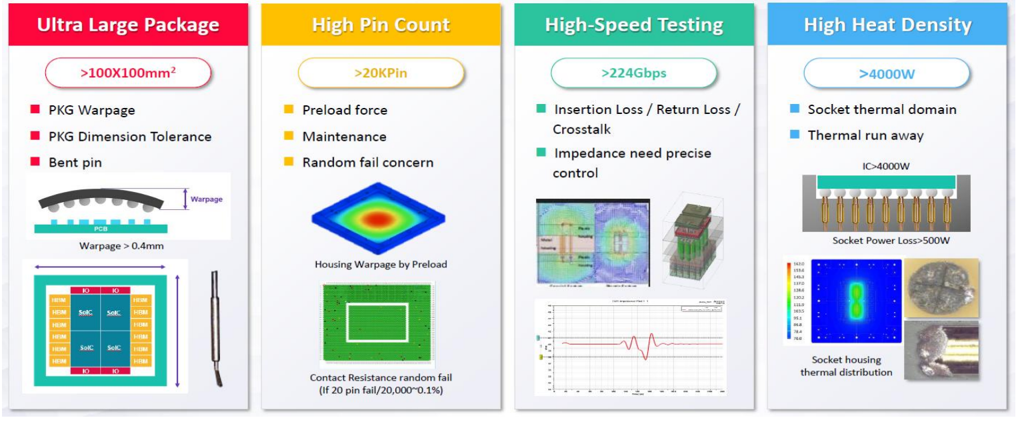
Source: Company data, Nomura research
High Heat Density
>4000W
Socket thermal domain
• Thermal run away
IC>4000W
Socket Power Loss>500W
....
Socket housing thermal distribution
"hultlanyoo are mulcauve, bounuareo
Nelweell aujavell leutmolgleo are tanomuon curleo whlere oorutorlo ovellay
Teot Haluwale ale ohlppeu velule ullp mlass pluuucllul
Cantilever (peripheral pad)
Fig. 134: Typical pitch regimes and corresponding test interface solutions
shipment
Pitch ranges are indicative; boundaries between adjacent technologies are transition zones where solutions overlap
+
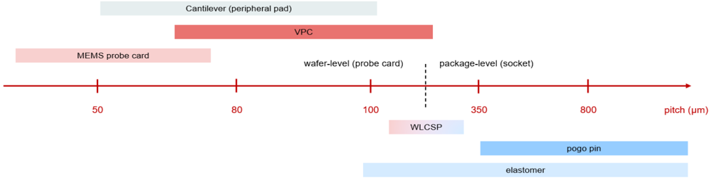
-12m
Test interface
Note: This is a conceptual illustration, not specific to any company or project. Source: Nomura research
Fig. 135: Timeline of testing equipment and interface preparation
Test hardware are shipped before chip mass production

Note: This is a conceptual illustration, not specific to any company or project. Source: Nomura research
+
+
10,000
9,000
8,000
7,000
6,000
5,000
4,000
3,000
2,000
1,000
ve coumate tmay leaul Jo ul tular levellue 1l 40401
6%
HyperSocket to bear fruit beyond 2027F
HyperSocket combines pogo pins and elastomer together to address larger and more complicated chip packages
HyperSocket is WinWay's next-generation test socket platform designed for ultra-large package, high-frequency and high-speed applications, targeting AI and HPC devices built on 2.5D/3D advanced packaging. The patented structure was developed to meet sensitive contact-resistance test requirements: it provides a soft contact interface that avoids damage to solder balls, and maximizes production efficiency. 2026F
Conventional elastomer sockets are constrained by film thickness, which limit vertical stroke/compliance (a growing problem as ultra-large AI packages suffer from warpage). Spring probe (pogo pin) sockets offer good compliance but limited contact quality (as a standard crown tip provides only 4-9 contact points per pin, which do not touch the solder ball simultaneously and potentially cap the achievable contact resistance and currentcarrying capability [CCC].) HyperSocket resolves this trade-off by using spring probes to provide stroke/compliance and an elastomer layer to provide surfacearea contact against the solder ball, delivering both low, stable contact resistance and tolerance for large-package warpage ; the platform also extends to dual-layer (upper/lower, e.g. HyperSocket-Dual Film) and liquid-cooled configurations.
Capacity constraint to cap revenue upside
WinWay sees strong demand from customers for HyperSocket to be adopted in mass production volume, and it gave large order projections as early as 2025. However, the current bottleneck mainly falls in elastomer capacity, as this has not been WinWay's focus in the past. Costs will likely be another consideration for customers, as the HyperSocket solution carries a higher initial investment than conventional sockets (HyperSocket ASP is 30% higher), and the elastomer layer also becomes a consumable, requiring periodic replacement.
However, we believe HyperSocket design would be more widely adopted when the package size exceeds 100100mm/120120mm, especially when pin count exceeds 10k20k, while current mainstream GPUs/ASICs substrate size has not yet exceeded the threshold (Fig. 136 ); thus pogo pins are still dominant solutions. We observe some nextgen chips roadmap is approaching the limit (such as upcoming AMD MI455 or TPUv9 series beyond 2027F). Larger package size is an unavoidable trend, and we expect HyperSocket penetration to gradually increase. Note that during 1H26 earnings call, WinWay management set 5% as the high-end segment revenue target for HyperSocket in 2027E. We believe a suitable timeframe to expect a meaningful revenue contribution (say 5% of total revenue) from HyperSocket could be in 2028-29F (considering less than 1% of total revenue contribution in 2025F, still in low-single digit in 2026F, and less than 5% in 2027F, on our estimates, Fig. 137 ).
Fig. 136: Key GPUs substrate size is growing We tentatively assume 80x115mm substrate size for Feynman
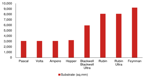
Source: Company data, Nomura estimates
Fig. 137: HyperSocket revenue contribution We estimate it may reach ~5% of total revenue in 2028F
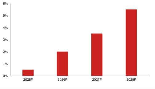
Source: Nomura estimates
2027F
2028F
Hyper-UF
Fig. 138: Comparison of different contact elements
CRS (Top)
Top
Housing
| Elastomer | Spring Probe | HyperSocketTM | |
|---|---|---|---|
| Travel (mm) | 0.2 ~ 0.3 | 0.6 ~ 1.0 | 0.6 ~ 1.0 |
| Contact Resistance (mΩ) @Recom. Travel | < 50 | < 60 | 25%↓ |
| Contact Resistance (mΩ) @0.15mm | < 50 | < 70 | 50%↓ |
| Force (g) @Recom. Travel | 40 ~ 85 | 10 ~ 35 | 10 ~ 35 |
| Current Capacity (A) | 2.4 | 3 ~ 3.5 | 5 ~ 6 |
| Applicable pitch range : 0.4~1.27mm | Applicable pitch range : 0.4~1.27mm | Applicable pitch range : 0.4~1.27mm | Applicable pitch range : 0.4~1.27mm |
Source: Company data, Nomura research
Fig. 140: Requirements for HyperSocket
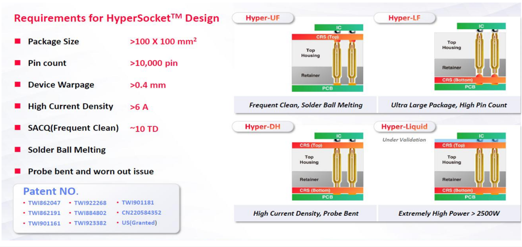
Source: Company data, Nomura research
Hyper-LF
Fig. 139: Illustration of HyperSocket
Retainer
Hyper-Liquid
Under Validation
Extremely High Power > 2500W
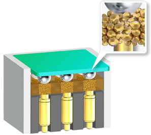
Source: Company data, Nomura research
Insertion 2
Insertion 3
Industry CPO progress worth tracking
Silicon Photonics (Siph)/CPO is another rising trend in semiconductor manufacturing. We have detailed our understanding of testing flows in CPO testing in our Anchor Report and in Fig. 141 . In May-2026, WinWay hosted a forum to discuss 'The Evolution of CoPackaged Optics (CPO) - Advanced Testing Methodologies for Silicon Photonics', in which it presented the reasons to adopt CPO, different approaches from various industry vendors, testing insertions flows, and WinWay's solutions. EIC Silicon
PIC
Our understanding of CPO testing insertion is as follows: Insertion 1 is PIC and EIC single-sided wafer-level test; Insertion 2 is double-sided wafer-level test after hybrid bonding; Insertion 3 may include two optical engine (OE)-level testing steps after singulation - before and after packaging (attach FAU [fiber array unit]/receptacle/structural reinforcements), and Insertion 4 is the module-level test after the optical engine is mounted on the substrate. WinWay showcased its WLCSP pitch probe head for EIC/PIC wafer/die testing, double-sided probing system, as well as optical engine (OE) test socket and HyperSocket.
While final testing flows and vendor selection could vary by customer, we expect WinWay to have more niche on socket opportunities in Insertion 3 and Insertion 4, namely after singulation, and more likely after packaging, as packaging-level-test has long been its core competency.
Our view on the CPO timeline now largely aligns with nVidia's product roadmap - for scale-out switch to ramp up in 2H26 along with Rubin platform (see 2026 GTC note ). However, given there are a lot of technical challenges for the brand-new architecture, we expect any large volume to come in 2027F and beyond, and the TAM will likely be further enlarged after CPO penetrates into scale-up (likely in Feynman).
Fig. 141: CPO insertion flow
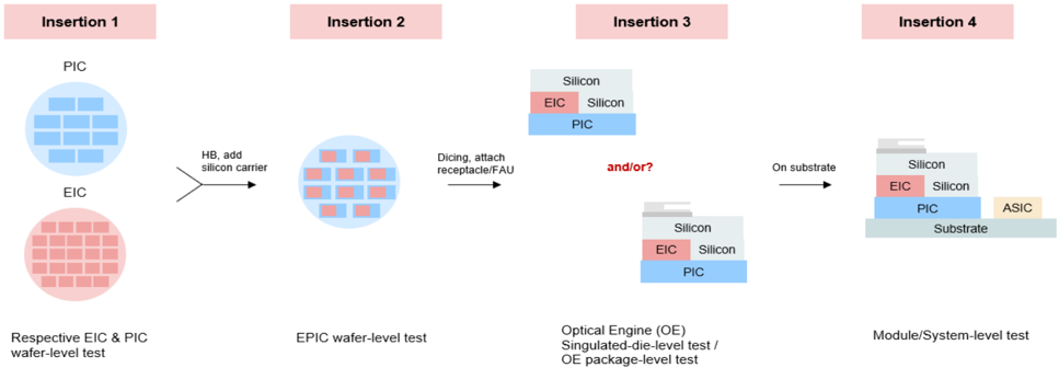
Note: This is a conceptual illustration, not specific to any company or project. Source: Nomura research
Fig. 142: CPO insertion flow and potential suppliers
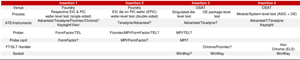
| Insertion 1 | Insertion 2 | Insertion 3 | Insertion 3 | Insertion 4 | |
|---|---|---|---|---|---|
| Venue | Foundry | Foundry | OSAT | OSAT | OSAT |
| Process | Respective EIC & PIC wafer-level test (single-sided) | EIC die on PIC wafer (EPIC) wafer-level test (double-sided) | Singulated-die- level test | OE package-level test | Module/System-level test (ASIC + OE) |
| ATE/Instruments | Advantest/Teradyne/Ficontec/Chroma? Keysight/Viavi | Teradyne/Advantest? | Advantest/Teradyne? | Advantest/Teradyne? | Advantest?/Teradyne Keysight |
| Prober | FormFactor/TEL | Ficontec/MPI/FormFactor/TEL? | MPI/TEL? | ||
| Probe card | FormFactor? | MPI/FormFactor? | MPI? | ||
| FT/SLT Handler | Chroma/Ficontec? | Hon Chroma (ELS) | |||
| Socket | WinWay? | WinWay | WinWay |
Source: Nomura research
Insertion 4
Silicon
EIC Silicon
PIC
ASIC
Substrate
Module/System-level test
More through sockel (not via prosing system, " our view)
'inWay
Package Level Test
Fig. 143: CPO test flow and WinWay's offerings
4007m
KIC
EIC/PIC
Die
CPC / CPO
LGA Side
Substrate
WLCSP Fine Pitch Probe Head
(EIC/PIC Wafer test)
Double Sided Probing System
Source: Company data, Nomura research nKCAN
Engine
CPO Substrate
CPO Module
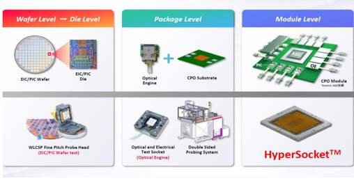
Source: Company data, Nomura research
Fig. 145: WinWay should play a role in package-level test
More through socket (not via probing system, in our view)
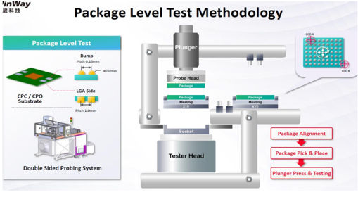
Source: Company data, Nomura research
Prond Hanc
Module Level
Twray
1 15
4 **
Module Level Test Methodology
Module Test
Die Level Test
Die Level Test Methodology
Test Requirement Test speed, Alignment, Mechanism Design.
Test Requirement Optical at TOP / Electrical at BTM.
Fig. 144: WinWay's probe card solution for die-level test
Fic/eio
EIC/PIC Wafer
WLCSP Fine Pitch Probe Head
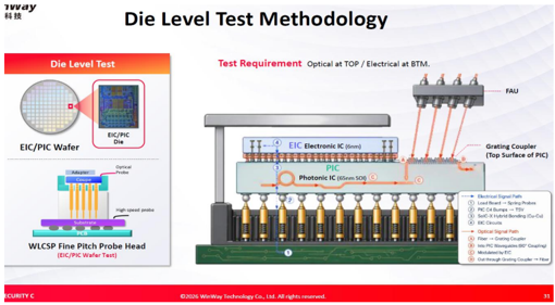
(EIC/PIC Wafer Test)
HyperSocket™
Source: Company data, Nomura research
Fig. 146: WinWay proposes HyperSocket for CPO module test
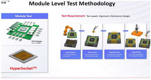
Source: Company data, Nomura research
1,300
1,100
900
700
500
300
Share price recap
B100 cancellation and GB push out
Farm-Payroll
Macro: BOJ, Non-
WinWay was listed in January 2021, but the share price was under pressure initially due to the US imposing restrictions on Huawei (unlisted), and thus it lost some business opportunities. Other than smartphone, PC/gaming was also a major part of its business. As the smartphone business gradually weakened, WinWay shifted gears to AI/HPC step by step. While WinWay's 2022 operating results showed a significant leap vs. 2021, the share price did not perform much due to overall peaking of the semiconductor cycle and macro headwinds. Finally, along with AI's emergence from end-2022, its share price started to climb. Despite the continued strong performance of AI/HPC into 2023, consumer electronics went through a severe inventory correction in 2023 (before bottoming out in 1Q24). That said, WinWay's share price still doubled from ~TWD400 from early-2023 to ~TWD800 at end-2023, benefiting from AI megatrend (vs. the TAIEX which rose 27% in 2023).
The AI/HPC socket business ramp-up brought its average monthly sales to ~TWD500mn in 2024 from ~TWD300mn in 2023. The probe card business further drove strong growth in 2025. Following its solid revenue expansion in 1Q25, the share price rose substantially (up 148% vs. the TAIEX up 26% in 2025). In 1H26, the share price rose sharply on increased expectations and enhanced visibility on upcoming key project ramp-up. It then started to decline from TWD9,000 in early July to TWD6,500 as of 22 July 2026, as rising macro risks and overall sentiment on AI has taken a slight turn amid concerns about New York's moratorium on data center de velopment and Meta's (META US, Not rated) initiatives around Meta Compute . We also note the recent share price pullback is potentially reacting to company-specific issues after the release of June quarter earnings, for which we observe likely worse-than-expected profitability.
Fig. 147: WinWay's share price events vs. monthly sales, 2023-24
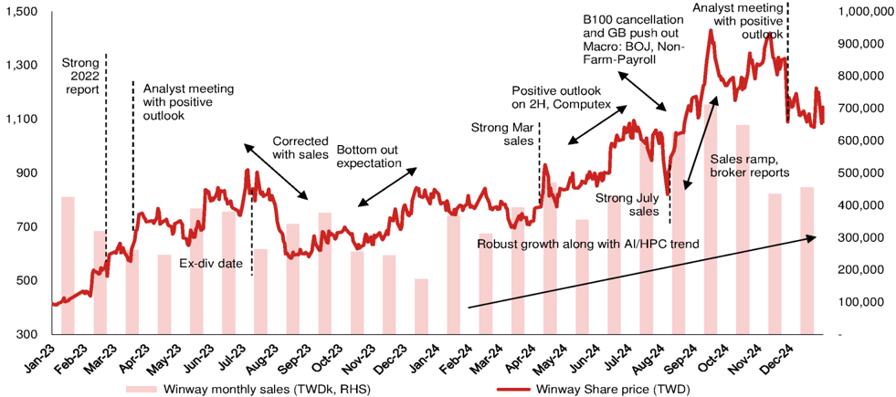
Source: TEJ, company data, Nomura research
Analyst meeting i with positive !
outlook
Sales ramp, broker reports
900,000
800,000
700,000
600,000
500,000
400,000
300,000
200,000
100,000
10,000
8,000
6,000
4,000
Fig. 148: WinWay's share price events vs. monthly sales, 2025-26 YTD
and CoWoS cut
Macro: tariff
Jan salesi
2,000
Jan-25
- visibility on Al projects,
Discussions on price hike
1,400,000
1,200,000
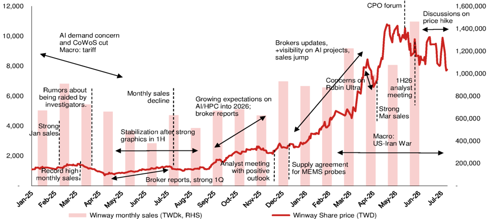
Source: TEJ, company data, Nomura research
Brokers updates, sales jump
CPO forum
Financial analysis and risks
We estimate a 69% revenue CAGR over 2026-28F
We expect the two largest segments - probe card and socket - to drive WinWay's revenue expansion in the next 2-3 years, as more and more AI/HPC projects are being added to the pipeline every day, driving higher volume demand and content value, with greater opportunities from additional test insertions such as BI/SLT and the emergence of CPO, and as WinWay itself also gains share from existing suppliers. Currently, due to the packed project pipeline, the largest revenue bottleneck is capacity. We believe WinWay will stay fully-utilized into 2027F (the company's capacity expansion plan is shown in Fig. 164 ), and pricing power could also improve amid the supply-constrained environment. We model WinWay's total revenue to grow by 84%/73%/65% in 2026F/27F/28F, at a 69% CAGR over 2026-28F, vs. 46% over 2023-25.
Temporary profitability headwinds; well-controlled opex to partly offset GM pressure
We estimate that the strong order momentum for MEMS probe card will temporarily temper WinWay's GM, and expect its GM to drop toward the low end of the 40-45% range in 2026F, vs. 45% in 2025. However, we expect that along with product mix improvement (more AI/HPC mix), better business value proposition, improving pricing power, and higher in-sourcing ratio, its GM will gradually get closer to 2025 levels in 2027-28F. We also expect operating leverage to materialize continuously in the forecast period, partially offsetting any GM pressure. We estimate a 94% EPS CAGR over 2026-28F, vs. 86% in 2023-25.
Fig. 149: WinWay's key financial figures
| 2023 | 2024 | 2025 | 2026F | 2027F | 2028F | 2026-28F CAGR | 2023-25 CAGR | |
|---|---|---|---|---|---|---|---|---|
| Key financial numbers (TWD mn) | Key financial numbers (TWD mn) | Key financial numbers (TWD mn) | Key financial numbers (TWD mn) | Key financial numbers (TWD mn) | Key financial numbers (TWD mn) | Key financial numbers (TWD mn) | Key financial numbers (TWD mn) | Key financial numbers (TWD mn) |
| Net revenue | 3,682 | 5,798 | 7,857 | 14,458 | 24,959 | 41,219 | 69% | 46% |
| y-y (%) | -28% | 57% | 36% | 84% | 73% | 65% | ||
| Gross profit | 1,365 | 2,534 | 3,556 | 5,925 | 10,876 | 18,409 | 76% | 61% |
| y-y (%) | -41% | 86% | 40% | 67% | 84% | 69% | ||
| GM (%) | 37% | 44% | 45% | 41% | 44% | 45% | ||
| Operating profit | 557 | 1,368 | 2,070 | 3,700 | 8,101 | 14,700 | 99% | 93% |
| y-y (%) | -59% | 146% | 51% | 79% | 119% | 81% | ||
| OpM (%) | 15% | 24% | 26% | 26% | 32% | 36% | ||
| Net profit | 464 | 1,186 | 1,673 | 3,157 | 6,641 | 11,935 | 94% | 90% |
| y-y (%) | -58% | 156% | 41% | 89% | 110% | 80% | ||
| EPS (TWD) | 13.52 | 34.31 | 46.93 | 88.32 | 185.76 | 333.86 | 94% | 86% |
| y-y (%) | -58% | 154% | 37% | 88% | 110% | 80% | ||
| Revenue mix (TWD mn) | Revenue mix (TWD mn) | Revenue mix (TWD mn) | Revenue mix (TWD mn) | Revenue mix (TWD mn) | Revenue mix (TWD mn) | Revenue mix (TWD mn) | Revenue mix (TWD mn) | Revenue mix (TWD mn) |
| Probe card | 251 | 641 | 2,308 | 4,176 | 7,323 | 11,705 | 67% | 203% |
| Contact element | 523 | 643 | 818 | 938 | 1,140 | 1,385 | 22% | 25% |
| Coaxial Socket | 1,485 | 2,632 | 3,386 | 6,606 | 12,754 | 22,937 | 86% | 51% |
| RF& Plastic socket | 806 | 1,199 | 721 | 2,232 | 3,117 | 4,398 | 40% | -5% |
| Burn-in socket | 387 | 267 | 293 | 146 | 187 | 261 | 34% | -13% |
| Others | 230 | 417 | 331 | 360 | 437 | 531 | 22% | 20% |
| Total | 3,682 | 5,798 | 7,857 | 14,458 | 24,959 | 41,219 | 69% | 46% |
| Revenue mix (%) | Revenue mix (%) | Revenue mix (%) | Revenue mix (%) | Revenue mix (%) | Revenue mix (%) | Revenue mix (%) | Revenue mix (%) | Revenue mix (%) |
| Probe card | 7% | 11% | 29% | 29% | 29% | 28% | ||
| Contact element | 14% | 11% | 10% | 6% | 5% | 3% | ||
| Coaxial Socket | 40% | 45% | 43% | 46% | 51% | 56% | ||
| RF& Plastic socket | 22% | 21% | 9% | 15% | 12% | 11% | ||
| Burn-in socket | 11% | 5% | 4% | 1% | 1% | 1% | ||
| Others | 6% | 7% | 4% | 2% | 2% | 1% | ||
| Total | 100% | 100% | 100% | 100% | 100% | 100% |
Source: Company data, Nomura estimates
40,000
14,000
40,000
35,000
35,000
12,000
30,000
10,000
30,000
25,000
25,000
20,000
20,000
8,000
6,000
15,000
15,000
4,000
10,000
10,000
2,000
5,000
5,000
Probe card +
coaxial socket:
20,000
400
100%
90%
18,000
350
16,000
300
60%
10,000
4,000
2,000
0%
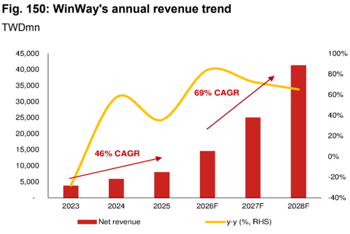
Source: Company data, Nomura estimates
Fig. 152: WinWay's annual operating profit trend
TWDmn
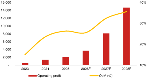
Source: Company data, Nomura estimates
Fig. 154: WinWay's annual product mix
TWDmn
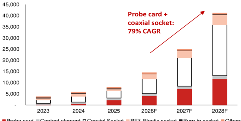
Source: Company data, Nomura estimates
40%
/0
150%
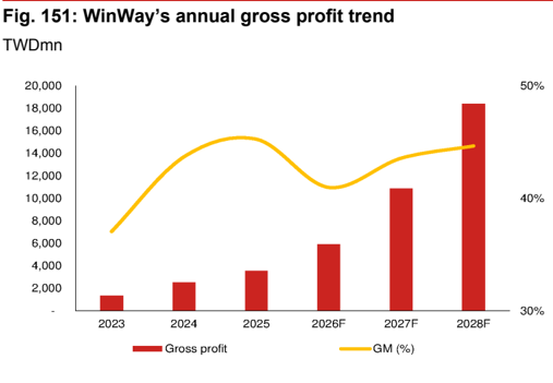
Source: Company data, Nomura estimates
Fig. 153: WinWay's annual EPS trend
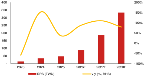
Source: Company data, Nomura estimates
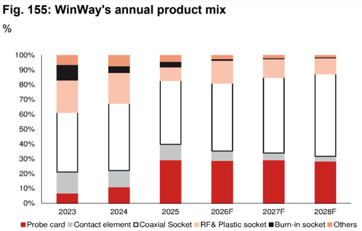
Source: Company data, Nomura estimates
Fig. 156: WinWay's P&L
| (TWD mn) | 1Q25 | 2Q25 | 3Q25 | 4Q25 | 1Q26 | 2Q26F | 3Q26F | 4Q26F | 1Q27F | 2Q27F | 3Q27F | 4Q27F | 2025 | 2026F | 2027F | 2028F |
|---|---|---|---|---|---|---|---|---|---|---|---|---|---|---|---|---|
| Net revenue | 2,297 | 1,522 | 1,804 | 2,234 | 2,980 | 3,523 | 3,881 | 4,073 | 5,098 | 5,911 | 6,582 | 7,367 | 7,857 | 14,458 | 24,959 | 41,219 |
| Gross profit | 1,120 | 746 | 759 | 931 | 1,282 | 1,398 | 1,560 | 1,684 | 2,206 | 2,564 | 2,881 | 3,224 | 3,556 | 5,925 | 10,876 | 18,409 |
| - OPEX | (393) | (286) | (352) | (457) | (505) | (528) | (581) | (610) | (612) | (709) | (790) | (663) | (1,487) | (2,224) | (2,774) | (3,710) |
| Operating profit | 728 | 460 | 407 | 475 | 777 | 870 | 979 | 1,074 | 1,594 | 1,855 | 2,092 | 2,561 | 2,070 | 3,700 | 8,101 | 14,700 |
| Net profit | 613 | 205 | 372 | 483 | 699 | 711 | 839 | 908 | 1,320 | 1,521 | 1,718 | 2,082 | 1,673 | 3,157 | 6,641 | 11,935 |
| EPS (TWD) | 17.21 | 5.76 | 10.43 | 13.56 | 19.54 | 19.90 | 23.47 | 25.41 | 36.93 | 42.55 | 48.05 | 58.23 | 46.93 | 88.32 | 185.76 | 333.86 |
| Profitability | 1Q25 | 2Q25 | 3Q25 | 4Q25 | 1Q26 | 2Q26F | 3Q26F | 4Q26F | 1Q27F | 2Q27F | 3Q27F | 4Q27F | 2025 | 2026F | 2027F | 2028F |
| Gross margin | 48.8% | 49.0% | 42.1% | 41.7% | 43.0% | 39.7% | 40.2% | 41.4% | 43.3% | 43.4% | 43.8% | 43.8% | 45.3% | 41.0% | 43.6% | 44.7% |
| Operating margin | 31.7% | 30.2% | 22.6% | 21.3% | 26.1% | 24.7% | 25.2% | 26.4% | 31.3% | 31.4% | 31.8% | 34.8% | 26.3% | 25.6% | 32.5% | 35.7% |
| Net margin | 26.7% | 13.5% | 20.6% | 21.6% | 23.4% | 20.2% | 21.6% | 22.3% | 25.9% | 25.7% | 26.1% | 28.3% | 21.3% | 21.8% | 26.6% | 29.0% |
| Q-Q | 1Q25 | 2Q25 | 3Q25 | 4Q25 | 1Q26 | 2Q26F | 3Q26F | 4Q26F | 1Q27F | 2Q27F | 3Q27F | 4Q27F | 2025 | 2026F | 2027F | 2028F |
| Net revenue | 49.3% | (33.7%) | 18.5% | 23.8% | 33.4% | 18.2% | 10.2% | 4.9% | 25.2% | 15.9% | 11.4% | 11.9% | ||||
| Gross profit | 52.5% | (33.5%) | 1.8% | 22.7% | 37.6% | 9.1% | 11.6% | 7.9% | 31.0% | 16.2% | 12.4% | 11.9% | ||||
| - OPEX | 15.9% | (27.3%) | 23.2% | 29.9% | 10.6% | 4.5% | 10.2% | 4.9% | 0.3% | 15.9% | 11.4% | (16.1%) | ||||
| Operating profit | 83.7% | (36.8%) | (11.4%) | 16.5% | 63.6% | 12.1% | 12.5% | 9.7% | 48.4% | 16.3% | 12.8% | 22.4% | ||||
| Net profit | 71.3% | (66.6%) | 81.4% | 30.0% | 44.5% | 1.8% | 17.9% | 8.3% | 45.3% | 15.2% | 12.9% | 21.2% | ||||
| Y-Y | 1Q25 | 2Q25 | 3Q25 | 4Q25 | 1Q26 | 2Q26F | 3Q26F | 4Q26F | 1Q27F | 2Q27F | 3Q27F | 4Q27F | 2025 | 2026F | 2027F | 2028F |
| Net revenue | 114.1% | 21.2% | (6.5%) | 45.1% | 29.7% | 131.4% | 115.2% | 82.3% | 71.1% | 67.8% | 69.6% | 80.9% | 35.5% | 84.0% | 72.6% | 65.1% |
| Gross profit | 140.9% | 38.2% | (4.4%) | 26.7% | 14.4% | 87.5% | 105.6% | 80.8% | 72.1% | 83.4% | 84.7% | 91.4% | 40.4% | 66.6% | 83.6% | 69.3% |
| - OPEX | 61.7% | 3.2% | 14.6% | 34.8% | 28.6% | 84.8% | 65.3% | 33.6% | 21.1% | 34.4% | 35.9% | 8.7% | 27.6% | 49.6% | 24.7% | 33.7% |
| Operating profit | 227.4% | 75.0% | (16.4%) | 19.9% | 6.8% | 89.2% | 140.3% | 126.3% | 105.3% | 113.1% | 113.7% | 138.4% | 51.3% | 78.8% | 118.9% | 81.4% |
| Net profit | 206.8% | (8.6%) | (8.0%) | 35.1% | 14.0% | 247.1% | 125.6% | 88.0% | 89.0% | 113.8% | 104.8% | 129.1% | 41.1% | 88.7% | 110.3% | 79.7% |
Source: Company data, Nomura estimates
Fig. 157: Nomura forecasts vs Bloomberg consensus estimates for 2026-28F
| 2026F | 2026F | 2026F | 2027F | 2027F | 2027F | 2028F | 2028F | 2028F | |
|---|---|---|---|---|---|---|---|---|---|
| (TWD mn) | NMR | BBG | Diff (%) | NMR | BBG | Diff (%) | NMR | BBG | Diff (%) |
| Net sales | 14,458 | 13,956 | 3.6 | 24,959 | 24,146 | 3.4 | 41,219 | 33,748 | 22.1 |
| Gross profit | 5,925 | 6,160 | (3.8) | 10,876 | 11,389 | (4.5) | 18,409 | 16,544 | 11.3 |
| Operating profit | 3,700 | 3,981 | (7.0) | 8,101 | 8,427 | (3.9) | 14,700 | 14,556 | 1.0 |
| Net profit | 3,157 | 3,399 | (7.1) | 6,641 | 6,778 | (2.0) | 11,935 | 11,712 | 1.9 |
| EPS (TWD) | 88.32 | 96.06 | (8.1) | 185.76 | 192.07 | (3.3) | 333.86 | 328.91 | 1.5 |
| Margin | NMR | BBG | Diff (%) | NMR | BBG | Diff (%) | NMR | BBG | Diff (%) |
| Gross margin (%) | 41.0 | 44.1 | (3.2) | 43.6 | 47.2 | (3.6) | 44.7 | 49.0 | (4.4) |
| Operating margin (%) | 25.6 | 28.5 | (2.9) | 32.5 | 34.9 | (2.4) | 35.7 | 43.1 | (7.5) |
| Net margin (%) | 21.8 | 24.4 | (2.5) | 26.6 | 28.1 | (1.5) | 29.0 | 34.7 | (5.7) |
Source: Company data, Bloomberg Finance L.P., Nomura estimates
100
400
350
80
300
60
250
200
40
150
20
100
0
Jul-22
50
0
40
12,000
Valuation methodology and risks
Our TP of TWD8,315 is based on 32x average 2027-28F EPS. Our 32x target multiple is in the middle of the stock's historical trading range over the past five years. The company traded between 14x and 40x during 2H22-1H25, before rising to 80-90x around May 2026. We believe the recent share price underperformance has improved the overall riskreward profile, and expect the company to be a major beneficiary of the ongoing AI trend given its business exposure to top GUPs and ASICs. We thus initiate coverage of the stock with a Buy rating, and view recent share price weakness as a good buying opportunity. · 2025E EPS 2026E EPS
Risks to our call
- 2028E EPS
Price (TWD; RHS)
Major downside risks to WinWay include: 1) weaker demand in AI/HPC market or slowdown of AI proliferation; 2) fierce competition in test interface market and share loss; and 3) worse-than-expected profitability
Fig. 158: WinWay's consensus 1BF P/E band
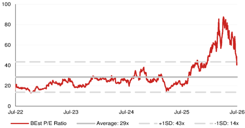
Source: Bloomberg Finance L.P., Nomura research
Fig. 159: WinWay's consensus 1BF P/B band
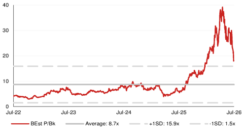
Source: Bloomberg Finance L.P., Nomura research
Fig. 160: WinWay's share price vs Bloomberg consensus EPS revisions
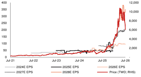
Source: Bloomberg Finance L.P., Nomura research
Jul-24
Jul-25
+1SD: 15.9x
Jul-26
- -1SD: 1.5x
Company profile
WinWay is one of the world's leading semiconductor test interface suppliers; it was ranked No.2 in the test socket market in 2025, according to Yole. Established in 2001 in Kaohsiung, WinWay started its business with test fixtures for optoelectronic products, and subsequently expanded into high-end test sockets for logic ICs, later adding probe cards and thermal control solutions. Currently, its major business operations include test sockets, probe cards, contact elements (probe pins), forming a one-stop test interface solution. WinWay was officially listed on the TWSE in 2021.
WinWay's products support broad-based applications including HPC/AI accelerators, CPU/GPU, mobile SoC, networking and automotive ICs, with particular strength in largesize, high-power advanced packaging devices. For capacity allocation, socket production is concentrated at its Kaohsiung headquarters (with new fab expansion underway), probe card production capacity is in Hsinchu, supplemented by service and engineering sites across the US, Europe, Japan, Korea, Singapore and China.
Fig. 161: WinWay board of directors
| Title | Name | Term (years) | Shareholding (%) | Experience |
|---|---|---|---|---|
| Mark Wang* | 3 | 13.33 | Chung Yuan Christian University, Department of Mechanical Engineering Manager, Manufacturing Department, ASE Test Engineer, Chunghwa Picture Tubes | |
| Cliff Liu | 3 | 3.09 | Master of Electrical Engineering, Rutgers University President, Premier Technology Political Science, National Taiwan University | |
| JQ Lee | 3 | 3.79 | Manager, Trust Department, China Development Industrial Bank CFO, Amtek SEMICONDUCTORS Consultant, Industrial Technology Research Institute | |
| Director | Jason Chen | 3 | 0.68 | Electronics, Lunghwa University of Science and Technology Sales Director, AzureWave Technologies Chief of Product Engineering, VIA Technologies IC Design Engineer, Syntek Semiconductor |
| CHIANG HOCK WOO | 3 | 0 | Bachelor of Science for Electrical, Engineering, University of Texas at Austin MBA, Sloan Fellow, Sloan School of Management, Massachusetts Institute of Technology Senior Vice President- Worldwide Sales & Service ,COHU, INC Director - Asia SOC Marketing & New Business Development, TERADYNE (ASIA) PTE LTD Managing Director, TERADYNE SHANGHAI | |
| Hsiu Yi Hung | 3 | 0 | Master of Law, National Chengchi University District court judge in Yunlin and Chiayi, Taiwan Public defender at the district courts of Penghu, Kaohsiung, Yunlin, and Pingtung, Taiwan | |
| Independent Director | Ted Lee | 3 | 0 | Business Administration, National Taiwan University President and General Manager, AzureWave Technologies Vice President, VIA Technologies Inc. |
| Wilson Wang | 3 | 0 | Department of Industrial Management, National Taiwan University of Science and Technology General Manager, LUMENTUM TAIWAN Co., Ltd. (Taiwan Branch) Yangzhou Yangjie Electronic Technology Co., Ltd. CEO | |
| Dennis Chang | 3 | 0 | Department of Accounting, Chung Yuan Christian University Senior Manager, Tax Department, Deloitte & Touche |
Note: *Representative of Hewei Investment Co., Ltd. Data as of Apr 2026.
Source: Company data, TEJ, Nomura research
vve collale lulal ovunel lavaully to uvuvie Ill CULOr
30
9
8
7
20
6
5
10
4
3
0
2
Jan-21
1
Fig. 162: WinWay's share price vs FINI holdings
2025
12,000
10,000
8,000
6,000
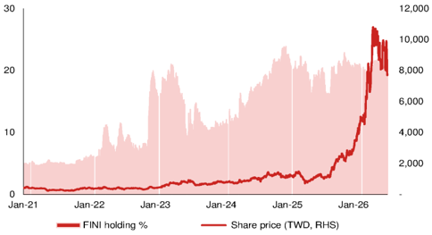
Source: TEJ, Nomura research
Fig. 164: WinWay's socket capacity
We estimate total socket capacity to double in 2026F
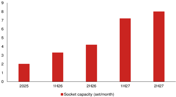
Note: 5,000-pin equivalent sockets
Source: Company data, Nomura estimates
Fig. 163: WinWay's top 10 shareholders
| Top 10 shareholders | % |
|---|---|
| Hewei Investment Co., Ltd. | 9.71 |
| JP Morgan investment account 2024 1st discretionary investment mandate for the New Labor Pension Fund | 8.3 |
| Hua Nan Commercial Bank as the custodian of the dedicated account of Allianz Tech Investors Taiwan Fund | 4.64 |
| JQ Lee | 3.79 |
| Liqin Investment | 3.22 |
| Cliff Liu | 3.09 |
| Citibank (Taiwan) Limited in custody of Norges Bank Investment Fund - JP MAME investment account managed by external managers | 3.01 |
| Liben International | 2.92 |
| Liquan Industrial | 2.92 |
| Mega International Commercial Bank as the custodian of the dedicated account of Allianz Global Investors Taiwan Fund | 2.43 |
Note: Data as of 18 Apr 2026.
Source: Company data, Nomura research
Relative performance chart
EQUITY: TECHNOLOGY
Price
(TWD)
8000-
7000-
6000-
5000
40001
3000
20001
-250
Ir-22s
-200
-175
-150
Hon. Precision, Inc. 7769.TW 7769 TT
EQUITY: TECHNOLOGY
Courna: | CEC Namiiral
Honing the edge of advanced silicon test
Beneficiary of structural AI/HPC testing growth and enabler of new technologies; initiate at Buy
Initiate coverage at Buy with TP of TWD11,100, implying ~73% upside
We initiate coverage of Hon. Precision (Hon) with a Buy rating and a target price of TWD11,100, based on 40x average 2027-28F EPS of TWD277. Our target P/E multiple is at the high end of Hon's historical trading band of 19-52x since its IPO, which we consider undemanding given a 58% net earnings CAGR through 2026-28F. The stock is currently trading at 29x 2027F EPS of TWD219, compared with semiconductor-backend equipment and test interface vendors (2027E Bloomberg consensus average P/E 37x). Hon is an equipment manufacturer focusing on IC test handlers and active thermal control systems (ATC) used in the final test (FT) or system level test (SLT), and AI/HPC/ASIC make up c.80% of its tool orders. We expect Hon to capitalize on an extended testing time for AI/HPC chips due to increased chip design complexity and larger package footprints, and increasing testing capex by AI OSATs and semiconductor manufacturing reshoring in the US indicate potential upside to Hon's ATC/handlers. We estimate Hon to record a revenue CAGR of 59% and model EPS at TWD134/TWD219/TWD336 for 2026-28F. A major downside risk to our view is CoWoS and backend testing capacity expansion slowdown.
Clear ATC upgrades down the road could boost ASP; handler upgrades in sight with new technologies on the horizon
A clear visibility of ATC roadmap and well execution, in our view, put Hon in a more favorable position for AI/HPC clients looking to initiate new chip development. We believe Hon should enjoy an ASP uptrend from AI/HPC customers' migration to more powerful ATC in view of increasingly stringent thermal requirements, and GPU-on-GPU SoIC stack for a leading AI GPU customer's 2028E platform could make such advancement more imperative. We also think OSATs may have to upgrade the handlers beyond 2027-28F for internal mechanics to support large packages (e.g., 10-11x reticle-size interposers, CoPoS, embedded multi-die interconnect bridge [EMIB]), and the emergence of copackaged optics (CPO) test insertions and micro-channel lids (MCL) could also drive new purchases of dedicated handlers. In addition to AI/HPC, we observe growing testing contents in mobile application processors (APs) and CPUs as well thanks to advanced packaging or multi-die layouts, and believe Hon should be a key beneficiary of a strong FT handler foothold in these areas.
| Year-end 31 Dec Currency (TWD) | FY25 Actual | Old | FY26F New | Old | FY27F New | Old | FY28F New |
|---|---|---|---|---|---|---|---|
| Revenue (mn) | 30,271 | 0 | 57,406 | 0 | 94,295 | 0 | 145,102 |
| Reported net profit (mn) | 12,362 | 0 | 24,182 | 0 | 39,375 | 0 | 60,563 |
| Normalised net profit (mn) | 12,362 | 0 | 24,182 | 0 | 39,375 | 0 | 60,563 |
| FD normalised EPS | 75.69 | 134.40 | 218.84 | 336.59 | |||
| FD norm. EPS growth (%) | 129.8 | 77.6 | 62.8 | 53.8 | |||
| FD normalised P/E (x) | 84.6 | - | 47.7 | - | 29.3 | - | 19.0 |
| EV/EBITDA (x) | 72.7 | - | 37.8 | - | 22.6 | - | 14.3 |
| Price/book (x) | 19.9 | - | 16.3 | - | 12.4 | - | 9.1 |
| Dividend yield (%) | 1.0 | - | 1.5 | - | 2.4 | - | 3.7 |
| ROE (%) | 34.5 | 37.6 | 48.1 | 55.3 | |||
| Net debt/equity (%) | net cash | net cash | net cash | net cash |
Source: Company data, Nomura estimates jul
Global Markets Research 24 July 2026
| Rating Starts at | Buy |
|---|---|
| Target price Starts at | TWD 11,100.00 |
| Closing price 22 July 2026 | TWD 6,405.00 |
| Implied upside | +73.3% |
| Market Cap (USD mn) ADT (USD mn) | 35,647.6 |
| 188.9 |
Relative performance chart
Source: LSEG, Nomura
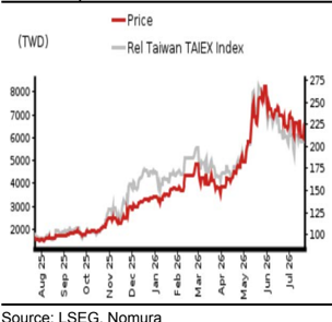
Research Analysts
Semiconductor
Eric Chen, CFA - NITB eric.chen@nomura.com +886(2) 21769965
Aaron Jeng, CFA - NITB
aaron.jeng@nomura.com +886(2) 21769962
Vivian Yang - NITB
vivian.yang@nomura.com +886(2) 21769970
Key data on Hon. Precision, Inc.
Performance
| (%) | 1M | 3M | 12M | ||
|---|---|---|---|---|---|
| Absolute (TWD) | -7.4 | 35 | 305.4 | M cap (USDmn) | 35,647.6 |
| Absolute (USD) | -9.3 | 31.4 | 269.6 | Free float (%) | 46.7 |
| Rel to Taiwan TAIEX Index | -1.3 | 16.6 | 210.4 | 3-mth ADT (USDmn) | 188.9 |
Income statement (TWDmn)
| Year-end 31 Dec | FY24 | FY25 | FY26F | FY27F | FY28F |
|---|---|---|---|---|---|
| Revenue | 13,992 | 30,271 | 57,406 | 94,295 | 145,102 |
| Cost of goods sold | -6,293 | -13,157 | -24,835 | -40,624 | -62,610 |
| Gross profit | 7,700 | 17,114 | 32,571 | 53,671 | 82,492 |
| SG&A | -1,415 | -2,068 | -3,613 | -5,752 | -8,416 |
| Employee share expense | 0 | 0 | 0 | 0 | 0 |
| Operating profit | 6,285 | 15,046 | 28,958 | 47,919 | 74,076 |
| EBITDA | 6,330 | 15,114 | 29,076 | 48,108 | 74,380 |
| Depreciation | -46 | -69 | -118 | -189 | -304 |
| Amortisation | 0 | 0 | 0 | 0 | 0 |
| EBIT | 6,285 | 15,046 | 28,958 | 47,919 | 74,076 |
| Net interest expense | 160 | 306 | 1,108 | 1,300 | 1,627 |
| Associates & JCEs | 0 | 0 | 0 | 0 | 0 |
| Other income | 239 | 232 | 179 | 0 | 0 |
| Earnings before tax | 6,683 | 15,584 | 30,245 | 49,219 | 75,703 |
| Income tax | -1,397 | -3,222 | -6,063 | -9,844 | -15,141 |
| Net profit after tax | 5,286 | 12,362 | 24,182 | 39,375 | 60,563 |
| Minority interests | 0 | 0 | 0 | 0 | 0 |
| Other items | 0 | 0 | 0 | 0 | 0 |
| Preferred dividends | 0 | 0 | 0 | 0 | 0 |
| Normalised NPAT | 5,286 | 12,362 | 24,182 | 39,375 | 60,563 |
| Extraordinary items | 0 | 0 | 0 | 0 | 0 |
| Reported NPAT | 5,286 | 12,362 | 24,182 | 39,375 | 60,563 |
| Dividends | -3,636 | -11,694 | -16,927 | -27,563 | -42,394 |
| Transfer to reserves | 1,650 | 668 | 7,255 | 11,813 | 18,169 |
| Valuations and ratios | |||||
| Reported P/E (x) | 194.4 | 84.6 | 47.7 | 29.3 | 19.0 |
| Normalised P/E (x) | 194.4 | 84.6 | 47.7 | 29.3 | 19.0 |
| FD normalised P/E (x) | 194.4 | 84.6 | 47.7 | 29.3 | 19.0 |
| Dividend yield (%) | 0.4 | 1.0 | 1.5 | 2.4 | 3.7 |
| Price/cashflow (x) | 445.3 | 64.6 | 56.5 | 34.5 | 22.7 |
| Price/book (x) | 75.4 | 19.9 | 16.3 | 12.4 | 9.1 |
| EV/EBITDA (x) | 181.1 | 72.7 | 37.8 | 22.6 | 14.3 |
| EV/EBIT (x) | 182.4 | 73.0 | 38.0 | 22.6 | 14.4 |
| Gross margin (%) | 55.0 | 56.5 | 56.7 | 56.9 | 56.9 |
| EBITDA margin (%) | 45.2 | 49.9 | 50.7 | 51.0 | 51.3 |
| EBIT margin (%) | 44.9 | 49.7 | 50.4 | 50.8 | 51.1 |
| Net margin (%) | 37.8 | 40.8 | 42.1 | 41.8 | 41.7 |
| Effective tax rate (%) | 20.9 | 20.7 | 20.0 | 20.0 | 20.0 |
| Dividend payout (%) | 68.8 | 94.6 | 70.0 | 70.0 | 70.0 |
| ROE (%) | 40.6 | 34.5 | 37.6 | 48.1 | 55.3 |
| ROA (pretax %) | 52.5 | 84.3 | 88.8 | 85.9 | 89.6 |
| Growth (%) | |||||
| Revenue | 47.5 | 116.3 | 89.6 | 64.3 | 53.9 |
| EBITDA | 66.6 | 138.8 | 92.4 | 65.5 | 54.6 |
| Normalised EPS | 72.3 | 129.8 | 77.6 | 62.8 | 53.8 |
| Normalised FDEPS | 72.3 | 129.8 | 77.6 | 62.8 | 53.8 |
Source: Company data, Nomura estimates
Cashflow statement (TWDmn)
| Year-end 31 Dec | FY24 | FY25 | FY26F | FY27F | FY28F |
|---|---|---|---|---|---|
| EBITDA | 6,330 | 15,114 | 29,076 -3,944 | 48,108 -6,161 | 74,380 -10,023 |
| Change in working capital Other operating cashflow | -3,509 -513 | 2,681 -1,610 | -4,734 | -8,544 | -13,513 |
| Cashflow from operations | 2,308 | 16,186 | 20,399 | 33,404 | 50,844 |
| Capital expenditure | -114 | -285 | -1,537 | -2,399 | -3,662 |
| Free cashflow | 2,193 | 15,901 | 18,862 | 31,005 | 47,182 |
| Reduction in investments | -1,196 | 1,218 | -7,847 | 0 | 0 |
| Net acquisitions | 0 | 0 | |||
| Dec in other LT | 0 | 0 | 0 | 0 | 0 |
| assets Inc in other LT liabilities | 0 0 | 0 0 | 0 0 | 0 | 0 |
| Adjustments | -11 | -364 | 331 | 0 | 0 |
| CF after investing acts | 986 | 31,005 | |||
| 16,754 | 11,346 | 47,182 | |||
| Cash dividends | -4,800 | -3,636 | -11,694 | -16,927 | -27,563 |
| Equity issue | 894 | 34,466 | 0 | 0 | 0 |
| Debt issue | 156 | -152 | 0 | 0 | 0 |
| Convertible debt issue | 0 | 0 | 0 | 0 | 0 |
| Others | -31 | 1 | 0 | 0 | |
| CF from financial acts | -5 -3,755 | 30,648 | -11,692 | -16,927 | -27,563 |
| Net cashflow | -2,769 | 47,402 | -346 | 14,077 | 19,619 |
| Beginning cash | 8,794 | 6,025 | 53,427 | 53,081 | 67,159 |
| Ending cash | 6,025 | ||||
| 53,427 | 53,081 | 67,159 | 86,778 | ||
| Ending net debt | -5,868 | -53,427 | -53,081 | -67,159 | -86,778 |
| Balance sheet (TWDmn) | |||||
| As at 31 Dec | FY24 | FY25 | FY26F | FY27F | FY28F |
| Cash & equivalents | 6,025 | 53,427 | 53,081 | 67,159 | 86,778 |
| Marketable securities | 2,020 | 801 | 8,652 | 8,652 | 8,652 |
| Accounts receivable | 2,913 | 2,935 | 7,438 | 11,760 | 18,614 |
| Inventories | 8,444 | 12,641 | 24,597 | 38,825 | 61,643 |
| Other current assets | 135 | 391 | 424 | 424 | 424 |
| Total current assets | 19,537 | 70,195 | 94,191 | 126,820 | 176,110 |
| LT investments | 81 | 174 | 212 | 212 | 212 |
| Fixed assets | 1,888 | 2,106 | 3,427 | 5,637 | 8,995 |
| Goodwill | 0 | 0 | 0 | 0 | 0 |
| Other intangible assets | 0 | 0 | 0 | 0 | 0 |
| Other LT assets | 360 | 795 | 624 | 624 | 624 |
| Total assets | 21,866 | 73,270 | 98,454 | 133,292 | 185,940 |
| Short-term debt | 157 | 0 | 0 | 0 | 0 |
| Accounts payable | 3,181 | 3,402 | 9,484 | 14,970 | 23,768 |
| Other current liabilities | 4,691 | 11,626 | 18,092 | 24,996 | 35,846 |
| Total current liabilities | 8,028 | 15,028 | 27,576 | 39,966 | 59,614 |
| Long-term debt | 0 | 0 | 0 | 0 | 0 |
| Convertible debt | 0 | 0 | 0 | 0 | 0 |
| Other LT liabilities | 106 | 211 | 296 | 296 | 296 |
| Total liabilities | 8,134 | 15,239 | 27,872 | 40,262 | 59,910 |
| Minority interest | 0 | 0 | 0 | 0 | 0 |
| Preferred stock | 0 | 0 | 0 | 0 | 0 |
| Common stock | 2,494 | 37,979 | 37,979 | 37,979 | 37,979 |
| Retained earnings | 11,182 | 19,908 | 32,398 | 54,846 | 87,845 |
| Proposed dividends | 0 | 0 | 0 | 0 | 0 |
| Other equity and reserves | 55 | 144 | 205 | 205 | 205 |
| Total shareholders' equity | 13,732 | 58,031 73,270 | 70,582 | 93,030 | 126,030 |
| Total equity & liabilities | 21,866 | 98,454 | 133,292 | 185,940 | |
| Liquidity (x) | |||||
| Current ratio | 2.43 | 4.67 | 3.42 | 3.17 | 2.95 |
| Interest cover Leverage | - | - | - | - | - |
| Net debt/EBITDA (x) | net cash | net cash | net cash | net cash | net cash |
| Net debt/equity (%) | net cash | net cash | net cash | net cash | net cash |
| Per share | |||||
| Reported EPS (TWD) | 32.95 | 75.71 | 134.42 | 218.87 | 336.64 |
| Norm EPS (TWD) | 32.95 | 75.71 | 134.42 | 218.87 | 336.64 |
| FD norm EPS (TWD) | 32.95 | 75.69 | 134.40 | 218.84 | 336.59 |
| BVPS (TWD) | 84.97 | 322.57 | 392.33 | 517.11 | 700.54 |
| DPS (TWD) | 22.50 | 65.00 | 94.09 | 153.21 | |
| Activity | 235.65 | ||||
| (days) Days receivable | 76.0 | 35.3 | 33.0 | 37.2 | 38.3 |
| Days inventory | 489.8 | 292.5 | 273.6 | 284.9 | 293.7 |
| Days payable | 184.5 | 91.3 | 94.7 | 109.9 | 113.2 |
| Cash cycle | 381.3 | 236.4 | 211.9 | 212.2 | 218.7 |
Source: Company data, Nomura estimates
Company profile
Founded in 1999, Hon. Precision (Hon) is a dedicated semiconductor equipment manufacturer focusing on IC test handlers and active thermal control systems (ATC) for IC backend testing. Hon's client base spans across major IC design houses, outsourced semiconductor assembly and test vendors (OSATs), and integrated device manufacturers (IDMs) worldwide.
Valuation Methodology
Our TP of TWD11,100 is derived from 40x average 2027-28F EPS, at the higher end of historical trading band (19-52x) since IPO. The benchmark of this stock is TAIEX.
Risks that may impede the achievement of the target price
Downside risks to our call include: 1) CoWoS and backend testing capacity expansion slowdown; 2) slower-than-expected product refresh, platform performance upgrade, or ramp-up by the AI chip end customers; 3) fiercer-than-expected market competition in test handlers; and 4) weaker-thanexpected end-market demand, particularly AI servers.
ESG
Hon. Precision has built its sustainability framework around three pillars: environmental protection based on the TCFD framework to assess energy/greenhouse gas management and water source risks, a "happy workplace" for employees, and social participation. All of these are overseen by a dedicated sustainable development unit that coordinates ESG risk responses and reports regularly to the Board of Directors.
Industry Supply Chain
(Final Test)
FT and SLT are Hon's equipment addressable markets Package FT IC
The semiconductor backend processes are punctuated by a few test insertions that sort out defective silicon as early as possible, serving as a gate to ensure output quality chip probe (CP), final test (FT), burn-in test (BIT), and system-level test (SLT) , and the entire backend flows start with CP at the wafer level before the individual dies are cut out of the wafer and undergo subsequent assembly (Fig. 165 ). A detailed description of the IC backend testing process is elaborated in our Anchor Report, and here we only focus on FT and SLT, which are Hon's addressable segments.
Fig. 165: An illustration of semiconductor manufacturing and backend testing flows
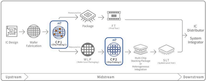
Source: CHPT, Nomura research
FT is a mandatory procedure , and depending on IC customers' configurations, there could be two or more FT steps during the manufacturing cycle (e.g., nVidia's [NVDA US, Not rated] AI GPUs require two FT steps, one before BIT and the other after BIT). FT is carried out after IC assembly (on substrates, lead frames, or wire bond) and chip packages are capable of accommodating larger input voltages or electric current than bare dies. FT measures electrical properties of chips given pre-programmed inputs to identify product functionality ('pass or fail' is the terminology) and sort functional products by grade (also known as 'binning'), all within the shortest possible time frame (usually hundreds or thousands of seconds) , as chip vendors may want to control test charges (measured by 'hourly rates') which are amortized expenses of costly testers.
There are three primary parameters that form a sequential filtering system in FT for logic circuits, and the focuses are on whether outputs are 'correct'. By contrast, analog/mixedsignal IC testing places more emphasis on the 'measurement accuracy' of select parameters (e.g. linearity and signal-to-noise ratio).
- Direct current (DC) test: The DC test is the first phase in FT and consumes the least time amongst the three phases. It measures the steady-state electrical characteristics of a chip using direct current and ensures the physical silicon structure is intact. The DC test does not validate logic or speed, however. The primary metrics measured during this phase include: 1) Open/Short test which verifies all pins are properly connected to the internal circuitry (no 'open') and that no pins are accidentally welded together (no 'short'); 2) Leakage current which ensures a pin does not 'bleed' excessive current into the substrate when it is given a specific voltage level; 3) Power consumption which detects electric current drain inefficiency; and 4) Output voltage level which confirms the chip can drive signals out at the correct voltage thresholds required to communicate with other components. 1.
- Function test: The subsequent function test is to check whether logic operation works properly. During the function test, the tester floods the chip with preprogrammed binary inputs (i.e., test vectors) and records the outputs generated by the chip to compare the results against the expected mathematical truth table. Function tests are typically executed at a nominal, conservative clock speed to isolate 2.
SLT Tester Site
Test
Program
High Speed Interface pure logical errors from high-speed timing anomalies.
Mock 1/0
- Alternating current (AC) test: The AC test introduces the critical dimension of 'time', evaluating how the chip performs under dynamic, high-frequency AC conditions and checking the output signals' 'waveform', because a chip might have perfect structure and flawless logic responses at slow speeds. AC test pushes the silicon to its physical limits by measuring sub-nanosecond timing parameters to ensure signals propagate cleanly across the die without corruption. Major test items include propagation delay, setup and hold times, rise and fall times, and maximum frequency. The AC test is also the foundation of 'binning' , sorting out the best-performing chips and lower-tiered ones. 3. Tester Hardware
On the other hand, SLT is an optional procedure , during which a chip is inserted into a system test board designated by a chip vendor to simulate how it works in the real-world scenario. The test board is a modified version of the actual commercial motherboard that eventually houses the silicon and is equipped with other components such as memory and peripherals. The SLT boots a full operating system like Linux or Android and runs heavy, asynchronous software workloads to replicate genuine user environments (Fig. 166 ). Throughout the process, SLT measures functional and behavioral metrics rather than raw structural data, including system stability, workload execution throughput, thermal throttling thresholds, and high-speed interface bit error rates (BER).
SLT has gained traction industry-wide because it exposes defect classes that the preceding stages structurally cannot (Fig. 167 ). DC test, Function test, and AC test are largely deterministic and exercise the device in isolation, at fixed patterns and controlled conditions. They are effective at catching hard, static failures but are poorly suited to intermittent, workload-dependent or interaction-level defects - issues only manifest when multiple IP blocks operate concurrently under realistic power, thermal, and timing stress, or under specific software-induced corner cases. As chip complexity has grown with heterogeneous integration, multi-core coherency, and higher-speed interfaces, these system-level 'test escapes' could result in a larger share of field returns, which has steered SLT from a niche practice in automotive/mobile applications toward broader adoption across compute, AI accelerator, and networking chips, where the cost of a return merchandise authorization (RMA) far outweighs the cost of additional test screening.
Fig. 166: SLT acknowledges that software is part of the system, and recreates the enduse environment as closely as possible
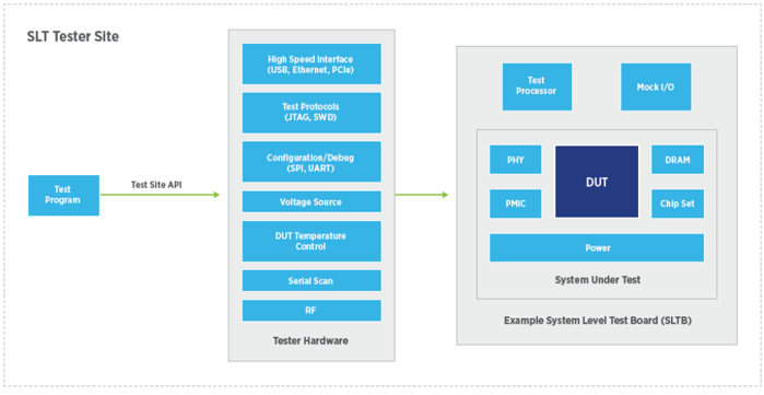
Source: Teradyne, Nomura research
FAB
ATE
Testing
Good Devices
Bad Devices
Assemble
ATE
System Level
SLT
Fig. 167: Traditional test coverage becomes more challenging, and SLT's strategic importance is emerging
At Risk
Weak
Healthy
System Level
Testing
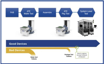
Source: Teradyne, Nomura research
The SLT phase is less expensive than FT given no usage of multi-million-dollar testers, but it is very time-consuming and could take minutes or even hours to execute per device. At high volumes, the throughput mismatch could become the binding constraint on SLT adoption, since running every unit through hours of system-level workloads is economically impractical for most product lines. As such, the industry leans toward parallel testing inside automated SLT handlers, and potentially the integration of adaptive testing backed by machine learning algorithm which selectively routes only silicons at risk to extended SLT screening while the bulk of the chips proceed through a shortened or standard flow (Fig. 168 ). This 'smart SLT' approach preserves most of the defectscreening benefit while containing the test time and cost overhead, and is emerging as a key differentiator among OSATs and IDMs competing on both quality (defined by defective parts per million, or DPPM) and test cost per unit.
Fig. 168: Adaptive SLT could further reduce the overall cost (time) of test
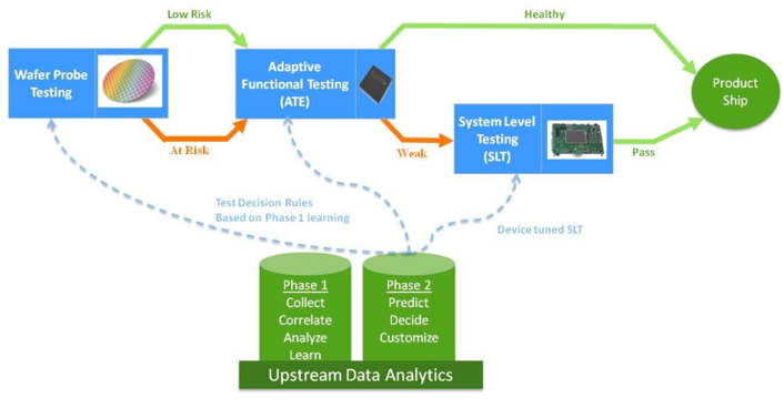
Source: AEM, Nomura research
IC test trios: ATE, prober/handler, and test interface
The semiconductor testing is not carried out by one single tool but a tightly integrated system also known as 'test cell'. The test cell consists of three major parts: automated test equipment (ATE), prober/handler, and application-specific test interfaces. In SLT, the ATE is replaced with a system test board on which test sockets are equipped, housed inside an SLT handler.
- Automated test equipment (ATE): ATE, or simply 'tester', is the sophisticated core workstation of the test cell that feeds precise electrical stimulus signals (e.g. voltages, currents, or high-frequency waveforms) into the device under test (DUT) and monitors the output responses. The tester compares the chip's real-time performance running on pre-programmed inputs against engineering design ·
(SLT)
Device tuned SLT
Pass
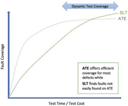
Fault Coverage
Dynamic Test Coverage
Test head
Opening/closing specifications to identify defectives. In the ATE architecture, the mainframe houses the tester's power supply, central cooling unit and the system controllers, and the test head houses the test interfaces. Wafer Test Head
- Prober/handler: The prober or the handler is the mechanical automation arm of the test cell that operates with the ATE to ensure a continuous, high-speed, and unmanned silicon test flow. The test head is flipped and pneumatically or hydraulically docked into the core mechanical nest of the prober/handler. The prober and the handler are used in different testing scenarios the prober is present in CP and handles uncut wafers, using microscopic pins to physically contact with individual die before they are singulated, while the handler picks up chip packages (in FT or SLT) from trays, inserts them into the test sockets, and physically sorts them into different bins based on the tester's verdict. ·
- Test interface: The test interface is the physical and electrical 'bridge', customized based on the silicon layout/package, to connect the generic tester to the DUT. A probe card paired with pogo pins (or MEMS pins for fine-pitch applications) is used in CP, while a load board with test sockets is adopted in FT. ·
Fig. 169: A test cell in chip probe
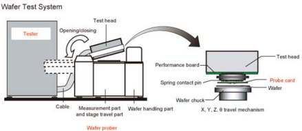
Source: MJC, Nomura research
The IC test squad is not complete without 'role players'
Beside the aforementioned trios, we note there are also tools supplementing temperature management to prevent undesired shifts in chip performance and physical properties under different thermal conditions, and specialized plug-in modules to expand or reconfigure the tester's scope.
- Thermal chuck: During CP, the chuck is the flat, rigid metallic platform that holds the silicon wafer in place using vacuum suction. A thermal chuck is a chuck with built-in heating elements and internal cooling channels to uniformly control the temperature of the wafer under test when mimicking different thermal conditions in operations. A thermal chuck must demonstrate extreme planarity (i.e., very meagre warpage) at extreme temperature swings to avoid poor electrical contacts or wafer crack by probe needles. ·
- Active thermal control system (ATC): ATC is a dynamic temperature management system integrated into the handler. When a tester boots up workloads, the DUT could undergo a spike in internal power density and instantaneously heat up. ATC detects the thermal conditions of the chip under test and instantly adjusts its cooling/heating action to counteract the chip's internal power fluctuations. ·
- Instruments: The tester is essentially a modular chassis populated by a cluster of instruments that define its initial testing scope. However, if a silicon requires test coverage beyond this built-in set, specialized instruments can be added to the tester to extend its capabilities. These modular instruments are notably critical for high-·
Fig. 170: A test cell in final test
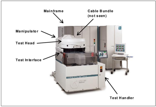
Source: SAE Technical Papers "Thermal Management and Control in Testing Packaged Integrated Circuit (IC) Devices", Nomura research
Mainframe
Cable Bundle
(not seen)
Test Handler
prober (right; by FormFactor)
Fig. 171: The thermal chuck is integrated into the wafer prober
Thermal chuck (left; by ATT Systems) and wafer prober (right; by FormFactor)
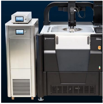
Source: FormFactor, Nomura research
Fig. 174: Semiconductor test equipment and interface maker overview
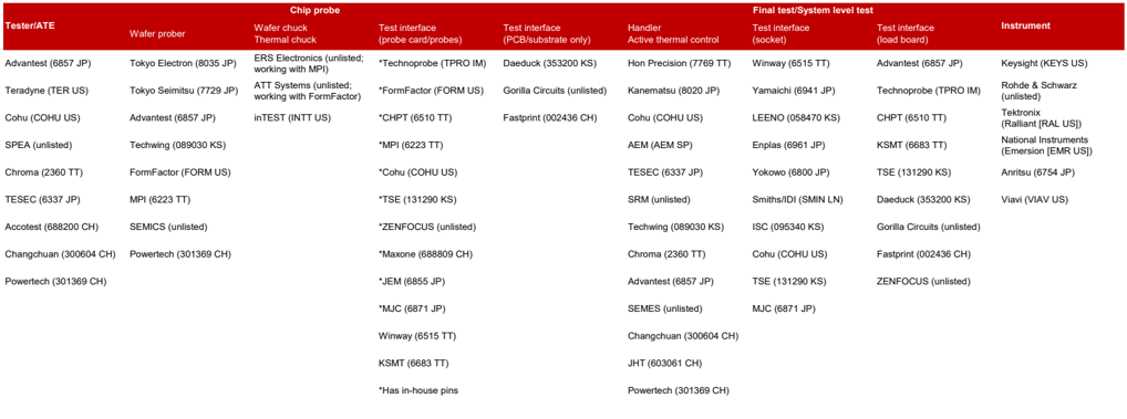
| Chip probe | Chip probe | Chip probe | Final test/System level test | Final test/System level test | Final test/System level test | Final test/System level test | Final test/System level test | |
|---|---|---|---|---|---|---|---|---|
| Tester/ATE | Wafer prober | Wafer chuck Thermal chuck | Test interface (probe card/probes) | Test interface (PCB/substrate only) | Handler Active thermal control | Test interface (socket) | Test interface (load board) | Instrument |
| Advantest (6857 JP) | Tokyo Electron (8035 JP) | ERS Electronics (unlisted; working with MPI) | *Technoprobe (TPRO IM) | Daeduck (353200 KS) | Hon Precision (7769 TT) | Winway (6515 TT) | Advantest (6857 JP) | Keysight (KEYS US) |
| Teradyne (TER US) | Tokyo Seimitsu (7729 JP) | ATT Systems (unlisted; working with FormFactor) | *FormFactor (FORM US) | Gorilla Circuits (unlisted) | Kanematsu (8020 JP) | Yamaichi (6941 JP) | Technoprobe (TPRO IM) | Rohde & Schwarz (unlisted) |
| Cohu (COHU US) | Advantest (6857 JP) | inTEST (INTT US) | *CHPT (6510 TT) | Fastprint (002436 CH) | Cohu (COHU US) | LEENO (058470 KS) | CHPT (6510 TT) | Tektronix (Ralliant [RAL US]) |
| SPEA (unlisted) | Techwing (089030 KS) | *MPI (6223 TT) | AEM (AEM SP) | Enplas (6961 JP) | KSMT (6683 TT) | National Instruments (Emersion [EMR US]) | ||
| Chroma (2360 TT) | FormFactor (FORM US) | *Cohu (COHU US) | TESEC (6337 JP) | Yokowo (6800 JP) | TSE (131290 KS) | Anritsu (6754 JP) | ||
| TESEC (6337 JP) | MPI (6223 TT) | *TSE (131290 KS) | SRM (unlisted) | Smiths/IDI (SMIN LN) | Daeduck (353200 KS) | Viavi (VIAV US) | ||
| Accotest (688200 CH) | SEMICS (unlisted) | *ZENFOCUS (unlisted) | Techwing (089030 KS) | ISC (095340 KS) | Gorilla Circuits (unlisted) | |||
| Changchuan (300604 CH) | Powertech (301369 CH) | *Maxone (688809 CH) | Chroma (2360 TT) | Cohu (COHU US) | Fastprint (002436 CH) | |||
| Powertech (301369 CH) | *JEM (6855 JP) | Advantest (6857 JP) | TSE (131290 KS) | ZENFOCUS (unlisted) | ||||
| *MJC (6871 JP) | SEMES (unlisted) | MJC (6871 JP) | ||||||
| Winway (6515 TT) | Changchuan (300604 CH) | |||||||
| KSMT (6683 TT) | JHT (603061 CH) | |||||||
| *Has in-house pins | Powertech (301369 CH) |
Source: Company data, Nomura research
Hon specializes in handlers and ATC, and provides tailored test kits
Hon has established itself as a powerhouse in the semiconductor backend testing arena, focusing specifically on AI/HPC and ASIC sectors. The company specializes in FT/SLT handlers ( more focus on FT ; primarily pick-and-place handlers, which use suction to transfer the DUT and press it into the test sockets) and ATC. Hon offers both dual-temp (high temperature [up to 170°C] and ambient temperature [around 25°C]) and tri-temp (high temperature, ambient temperature, and low temperature [down to -70°C]) ATC capabilities, based on three types of cooling system:
- Liquid-cooling (ATC3 series) supports a cooling capacity of up to 3,000W and a temperature control range of 25°C-150°C. AI GPUs and most AI ASICs adopt ATC3. ·
- Refrigerant-cooling (ATC5 series) supports a cooling capacity of 50-4,000W and a temperature control range of -70°C-175°C. Select AI ASIC customers and chips with ·
Tester+ FT Handler+ATC System
Tester
FT Handler
Fig. 172: The ATC is integrated into the handler
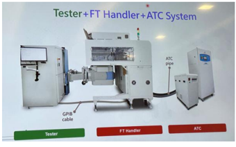
Source: Company data, Nomura research
ATC
WV KEYSIGHT
performance domains like analog/mixed-signal and high-speed digital, and we observe optical instruments are introduced in CPO test insertions to assist with photonic test items (e.g., optical insertion loss, spectrum/wavelength and polarization effects). GPIB
cable
UF2000
Fig. 173: The instrument helps expand dedicated test coverage
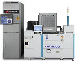
Source: Keysight, Nomura research
ATC5.5
Socket
-70°C
IS 7A9 83:
- ASIC
Dual-Temp
AI (GPU)
HPC
SLT ATC
application scenarios in radical environments (e.g. automobile and space) adopt ATC5. ATC6 7 21| @300W 125'C @30W 130'C @300W 175C FT ATC
25°C
ATC3.5
@2000W 125°C|
ATC3.3
125°C
130°C
150°C
ATC5.5
175°C
FT ATC
SLT ATC
- Air-cooling (ATC6 series) supports a cooling capacity of 30-50W and a temperature control range of 25°C-130°C. ATC6 could be used in low-power applications like Android APs. · ICH F
Socket
Load Board
Source: Company data, Nomura research
Sourca. Comnany data Mamura raccarch
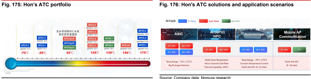
Source: Company data, Nomura research
In addition to the standalone machinery, Hon has a highly integrated test support ecosystem by selling socket layout kits (SLKs) and cold plates that are customized based on chip microstructure to guarantee an optimized contact force (Fig. 177 ). Hon typically derives c.20% of revenue from jigs and modules, which we believe the bulk is cold plates. SLK is a mechanical conversion interface to help a handler adapt to test module changeover on a test head for precise electrical connections. A cold plate is installed onto the SLK to help with thermal transfer during the test stage.
The majority of Hon's cold plates have a channel pitch of 500um. While AI/HPC chip thermal design power (TDP) continues to skyrocket, thermal dissipation during the test stage becomes an issue, and the convective heat transfer coefficient is the predominant factor of liquid cooling performance; it is also inversely correlated to channel pitch. Hon therefore introduced a microchannel cold plate (MCCP) in 2Q26, which can shrink the channel geometry to 150-200um. We think Hon could enjoy a 15% higher ASP from MCCP vs. mainstream cold plates.
Fig. 177: Hon's product offerings include IC test handler, ATC, SLK, and cold plates
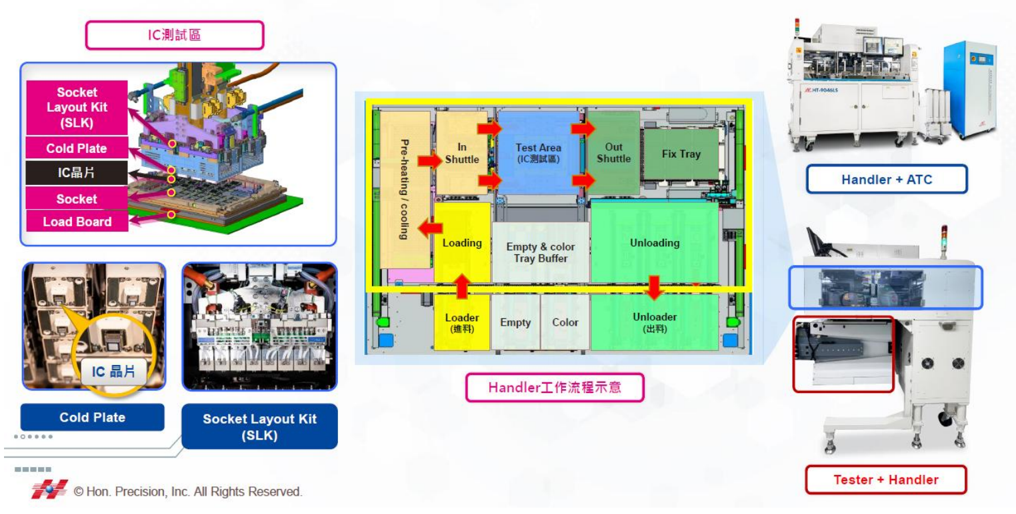
Source: Company data, Nomura research
IC. at ba
Tri-Temp
Non-ATC
Automotive
FT ATC
SLT ATC
Temp Range: -70°C~175°C
Junction Temperature Control
Multi-Site ATC (8-32 sites) |
Handler + ATC
Mobile"AP
Communication
FT ATC
Multi-Site ATC
(8~16 sites)
80%
60%
40%
20%
0%
Fig. 178: Hon's revenue mix
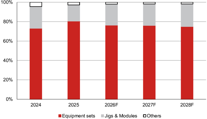
Source: Company data, Nomura estimates
advanced nodes
800
700
600
500
400
300
200
100
0
Normalized Cost/yield mm
5.0
N-7
Technology Scaling Propels Energy Efficient Compute
Rising design complexity and expanded footprints of AI/HPC chips spur structural testing growth 350 300
AI/HPC applications continue to lengthen testing time
N-4
We believe rising chip design complexity and expanded package footprints are the two most critical catalysts driving AI/HPC chips to foster structural growth in the semiconductor testing process, an often overlooked element in the manufacturing value chain because of its relatively low proportion in cost structure. The semiconductor industry is currently undergoing a paradigm shift in layout/architecture by embracing chiplet-based design philosophy, 2.5D advanced packaging to stitch multiple-reticle-sized interposers and 3D IC stacking to increase performance per area (measured by transistor density), as conventional geometric scaling slows, costs for chip design and yielding large die continue to rise at more advanced logic nodes (Fig. 179 , Fig. 180 , and Fig. 181 ), and any single chip inevitably faces the physical limit of reticle size (26x33mm exposure field size, or 858mm 2 ). In a seminar at SEMICON Taiwan 2025, TSMC (2330 TT, Buy) estimated compute performance per reticle improvement by 80x from N28 to A16, and the incorporation of advanced packaging could enlarge the gain to ~320x at >9.5x-reticle CoWoS (Fig. 182 ). 2012 CoWos N5
Fig. 179: The cost per yielded die vs node migration The cost per yielded die continues to increase when entering into more
advanced nodes
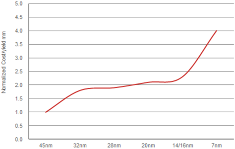
Source: Nomura research
Fig. 181: Skyrocketing chip design cost moving to more advanced nodes
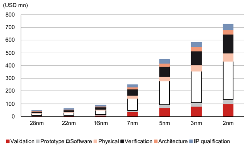
Source: IBS, Nomura research
Advanced
Packaging
0.77X~0.81
~80X
A16
2018
2020
Tows trop
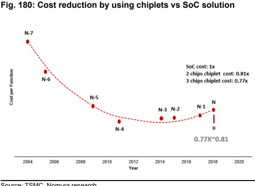
Source: TSMC, Nomura research
Fig. 182: Advanced packaging is an approach to bring the subsystem performance further up
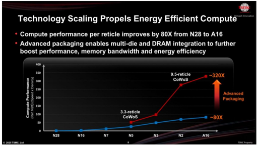
Source: TSMC, Nomura research
SoC cost: 1x
3 chips chiplet cost: 0.77x
2 chips chiplet cost: 0.81x
9.5-reticle
~320X
CoWoS
N
N-3 N-2
N3
2014
N2
2016
N-1
80%
60%
40%
20%
0%
fundamentally altered the economics and mechanics of semiconductor manufacturing. Die-to-die interconnect in chiplets or 2.5D/3D packaging is a complex jigsaw puzzle replacing traditional seamless on-die communication, because engineers must ensure robust signal and power integrity , and thermal management and mechanical stress control also become crucial in such layouts. Consequently, semiconductor testing is no longer just a routine quality-control process at the end of the production flows; it has become an indispensable, high-stakes discipline that directly dictates commercial success.
Device complexity increase will require a longer testing time by nature, and if we take nVidia AI GPUs as an example and index the FT time of Hopper to 1, we estimate 4x for Blackwell and ~7x for Rubin. The prolonged testing time and higher hourly rates should add to testing content in the cost structure, and we estimate the testing content (defined as the sum of FT, BIT and SLT) in nVidia Rubin could rise to 3.3% of the cost vs. 2.5% for Blackwell and 1.9% for Hopper, leveraging our supply chain analysis. A lengthening testing time presents an outright tailwind to semiconductor testing equipment makers, in our view, given the need by OSATs to keep up with throughputs.
Fig. 183: Increasing testing content in the logic manufacturing cost of nVidia AI GPUs
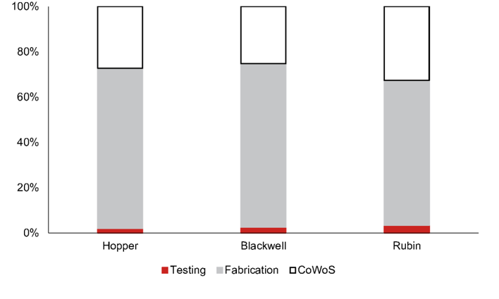
Source: Company data, Nomura estimates
AI/HPC chips are larger - handler redesign becomes imperative
We highlight that FT handlers could eventually undergo mechanical redesign and OSATs have to upgrade the tools if chip packages expand to a certain bar. Thus far, AI/HPC is the primary driver of package footprints. With logic dies already approaching a physical limit closer to the reticle size, nVidia and other AI accelerator makers understand incremental performance gains must come at the sub-system level rather than the chip level, and consequently are targeting to stack more logic dies and more HBM cubes onto interposers to construct a more powerful computing chip system. nVidia has moved from Ampere/Hopper (both 2x reticle-size interposer), to Blackwell in 2024 which houses two reticle-size compute complexes and eight HBM cubes on a 3.3x reticle-size interposer, and soon to Rubin in 2026E which houses two reticle-size compute complexes, two I/O dies, and eight HBM cubes on a 5x reticle-size interposer.
We believe the horizontal expansion of AI chip footprint is unlikely to halt as TSMC continues to unfold its CoWoS roadmap to introduce larger interposers (and therefore larger IC substrates underneath). According to TSMC, it is bringing 5.5x reticle size CoWoS into production in 2026 with a >98% yield. Previously, TSMC suggested its 9.5x CoWoS-L with SoIC and 12 HBM stacks would enter production in 2027E (Fig. 184 ; Tech Symposium 2025 ), and during the symposium this year, the company extended the roadmap to 14x reticle size CoWoS (20 HBM stacks) production by 2028 and aims for >14x reticle size CoWoS (24 HBM stacks) in production by 2029 (Fig. 185 ).
Interposer Size
Cowos-S
CoWoS-UR
coWos-s
1.5-reticle
N16 SoC
4 HBM2
258x537.6mm and the right one measures to 380x387.6mm
CoWoS® Enables Al Compute Scaling
Maller
CoWos® Enables Al Compute Scaling
4 3.0, 45-
• World's largest 5.5-reticle size CoWo in production with >98% yield in 2026
Fig. 184: TSMC's CoWoS roadmap laid out in 2025 Technology Symposium
9.5-reticle
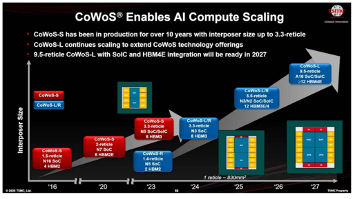
Source: TSMC, Nomura research
We note 'the bar' is correlated to 'how many chip packages that a matrix tray can accommodate' during the FT stage. A matrix tray is a plastic carrier that holds IC packages in a rigid grid of rows and columns, and the robotic arm of a handler will move the vacuum suction nozzle over the input matrix tray, suctions up untested chips (DUT), and places DUT into the test socket. The dimension of the tray generally conforms to the standard proposed by the Joint Electron Device Engineering Council Solid State Technology Association (JEDEC in short). The current standard tray is specified at 135.9x322.6mm , but if a chip package measures 120x125mm, one standard tray can carry only two pieces of DUT. The JEDEC acknowledges the industry trend of moving toward larger package footprints (notably in recent years, propelled by AI/HPC), and has added two new types of tray (also known as 'mega tray') in recent issues: 258x537.6mm and 380x387.6mm .
Hon has progressed the development of large-package handlers based on the new JEDEC standards, and the current planning is to begin shipments of tools capable of handling >120x150mm packages in 2H26E, and a handler solution for 250x250mm package in 2H27E, to position itself early for the next round of handler upgrades. Hon also targets to add more automation functionalities for better integration with unmanned factories (e.g., overhead hoist transfer [OHT] and autonomous mobile robot [AMR]) to boost throughputs. Our 'napkin math' indicates that a 120x150mm package could house an interposer sizing up to 10-11x reticle, which ties with TSMC's CoWoS roadmap in 2027-28, whereas our supply chain checks have not yet picked up such a large AI chip in the pipeline.
Fig. 186: IC matrix tray
Source: Sunrise, Nomura research
Fig. 187: JEDEC adds two new types of tray to address larger package size The left one is the current standard tray (135.9x322.6mm), and the one in the middle measures to
258x537.6mm and the right one measures to 380x387.6mm
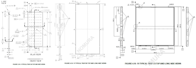
Source: JEDEC, Nomura research
AI/HPC chips are also hotter - more powerful ATC is necessary
We believe Hon will capitalize on the ASP uptrend from AI/HPC customers' migration to more powerful ATC (greater cooling capacity), since the sub-system performance gain from more dies in a package comes at the cost of more stringent thermal requirements.
Using nVidia AI GPUs as an example, the maximum TDP of Blackwell Ultra (B300) is
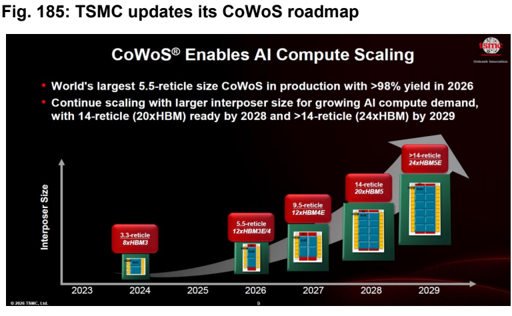
Source: TSMC, Nomura research
Source: TSMC, Nomura research
Besomi
2.5D vs. 3.5D Packaging
1,400W, which can be supported by Hon's ATC3.5 (cooling capacity of up to 2,000W). However, we think the TDP of Rubin (R100) may start from 1,800W, leaving little margin for ATC3.5 and likely initiating an upgrade to ATC3.6 (up to 3,000W). Admittedly, comparing TDP to ATC maximum cooling capacity is sometimes more biased than 'power density' (also better known as 'heat flux' in thermal physics), because TDP only tells us 'how much heat is generated' and power density/heat flux provides us 'how concentrated the hotspot is' and 'how fast the heat transfer is'. Metrics Face to Back connections via HCB
We foresee further elevating thermal challenges moving to Feynman (F100), slated to come onstream in 2028E. nVidia at GTC unveiled its plan to adopt 3D stacking starting from the Feynman platform (report ). Vertical chip stacking (SoIC platform at TSMC) theoretically could augment transistor counts per package, an outright indicator of computing power, without extra footprints (vs CoWoS/2.5D packaging that expands horizontally to accommodate more chips). AMD (AMD US, Not rated) believes 3.5D chip modules (i.e., 2.5D packaging + 3D hybrid bond) could enable shorter data paths and improved interconnect energy efficiency, and estimates ~80% more active silicon in a given module footprint than sheer 2.5D packaging (Fig. 188 ). We think the 3D logic stacking approach may also lie in other custom AI chip future roadmap (Fig. 189 ).
Currently, AMD leads the adoption of SoIC at TSMC (starting from MI300-series), and in the latest MI450, we believe AMD stacks four top dies (four XCD) on two reticle-sized active interposers (I/O dies), in which each top die scales to about 1/3 reticle size (Fig. 190 ). nVidia will be more aggressive in chip specs by stacking a reticle-sized GPU die on top of another for the Feynman platform, the first-ever GPU-on-GPU SoIC stacking ( report ), which would lead to higher computational power even with limited growth in interposer reticle stitching size (c.6x reticle, see footprint in Fig. 191 ; up from c.5x in Rubin). Such an industry practice theoretically exacerbates thermal dissipation challenges, and we expect it could trigger a migration to more powerful ATC3.7 . According to Hon, it has ATC with a maximum cooling capacity of up to 7,000-8,000W ready, and is working on engineering en route to >10kW (Fig. 192 ).
Fig. 188: 3.5D packaging offers a more dense chiplet module
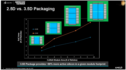
Source: AMD, Nomura research
Fig. 189: Broadcom introduced face-to-face 3D hybrid bond on its 3.5D platform
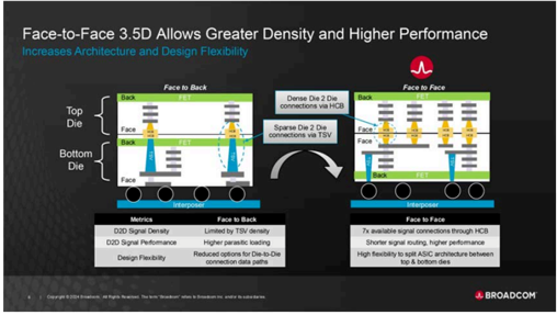
Source: Broadcom, Nomura research
W.
its 3.5D platform
Dense Die 2 Die
Back
Face
Face
Face to Face
7x available signal connections through HCB
Shorter signal routing, higher performance
High flexibilty to split ASIC architecture between top & bottom dies
1 BROADCOM
Face to Face
Dummy
HBM4
HBM4
HBM4
Dual-temp
HBM4
(25~150°C)
Power Density
HBM4
XCD
(N2)
HBM4
Tri-temp
(-80~180°C)
HBM4
Fig. 190: Floorplan of AMD MI455 and cross section
(N2)
Reconstituted interposer (5.5x ret.)|
B series
R series
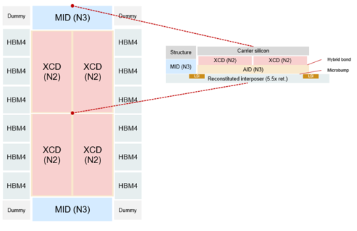
Source: Company data, Nomura research
SiC thermal plate to function as an intergrated silicon carrier (fill up the
Tell o
1/O
HBM4E
HBM4E
1/0
Fig. 191: The floor plan and cross-section chart of nVidia's Feynman GPU
SiC thermal plate to function as an intergrated silicon carrier (fill up the height gap in between GPU and HBM) and thermal interface material (TIM)
HBM4E
Structure
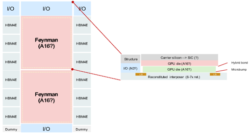
Source: Company data, Nomura estimates
Fig. 192: Hon's ATC roadmap to address greater TDP by AI/HPC chips
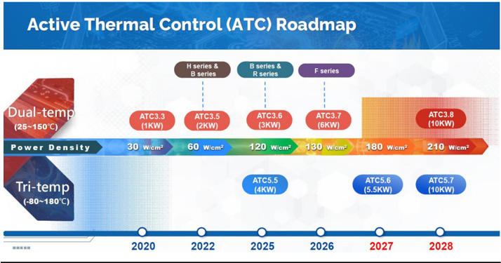
Source: Company data, Nomura research
Intel's EMIB might open a new window for large AI chip test demand
We believe some AI ASIC customers might have started evaluating Intel's (INTC US, Not rated) EMIB-T (embedded multi-die interconnect bridge with TSV) as a logic+HBM integration alternative because of concerns about insufficient capacity support at TSMC. According to Intel, EMIB-T targets HBM4/4E and logic chiplet interconnectivity with the lowest possible cost, and the company's roadmap is to scale to the integration of >8x reticle size total top silicon area on a ~120x120mm substrate by 2026E and >12x reticle size top silicon area on a >120x180mm substrate by 2028E (Fig. 193 ). If successful, Intel' s EMIB-T might open a new demand window for large AI chip testing. We reckon that Hon should have FT handlers under engineering verification at Intel Foundry.
We think Google's (GOOGL US, Not rated) potential reliance on Intel's EMIB-T for the next-generation TPU v9 (partnering with MediaTek [2454 TT, Buy]) could be a critical litmus test for Intel's advanced packaging capabilities. Based on our supply chain analysis, this signpost project will feature a substrate body size within 120x120mm (see the floor plan in our report ), not yet necessitating the transition to mega tray configuration.
A (much) less important side project at Intel EMIB might be Intel's laptop SoCs that will incorporate nVidia's RTX dies using NVLink, as a result of their partnership (report ). As Hon has been an important FT handler supplier for computing applications for years, we believe Hon might have potential to participate in this client CPU project, likely at a higher price than those shipped to Taiwan-based OSATs.
HBM4
Microbump
F series
Dummy
Ny Min
-4x
Reticle
Fig. 193: EMIB roadmap
-80x80
8
12
-8x
-120x120
Package size
intelfoundry
2028 +
-120*x180+
24
Future
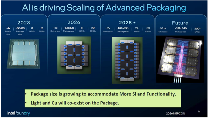
Source: Intel, Nomura research
Continued CoWoS capacity growth at TSMC, fueled by AI/HPC
We think TSMC's CoWoS capacity growth is one proxy for Hon's handler sales volume trend as both are primarily fueled by AI/HPC demand, and we estimate ~100% of CoWoS capacity each year is allocated to AI/HPC applications (vs. c.80% of Hon's handler tool orders come from AI/HPC). But we note that there is not necessarily a mathematical relationship between CoWoS capacity builds and handler purchases given varying output per interposer wafer for different AI accelerators and the throughput factor in handlers.
To date, TSMC's supply is apparently still constrained across the front-end and the backend given the demand strength from AI, and the company has expressed its commitment to expanding its capacity in due course, citing that it 'works very hard to meet all the demand ' and 'doesn't leave any business on the table ' (see remarks from 4Q25 and 1Q26 results ). We observe TSMC has turned more aggressive on CoWoS capacity planning (or more precisely, 'CoW' capacity) in recent months in response to surging AI chip demand, and lifted the capex guidance again in the July earnings call (report ), which should indirectly underscore the growth trajectory of Hon's handler business.
In our most recent Asia AI Semi & Server Anchor Report , our supply chain checks suggest TSMC will likely expand its CoWoS capacity to 1,100kpcs in 2026F (or c.130kwpm by the end of 2026F) and bring this up to 2,000kpcs in 2027F. Although TSMC has turned more aggressive in its CoWoS plan, our contrarian view is that 'WoS' (not controlled by TSMC) and many small components (e.g. IC substrates) would very likely become a bigger bottleneck than 'CoW' (controlled by TSMC) in 2027F. We only assume 1,800kpcs of CoWoS output in 2027F (despite our assumption of a TSMC target of 2,000kpcs).
While we have no clear bottom-up estimates about how TSMC is going to expand its CoWoS capacity beyond 2027F, we had tried to triangulate a possible trajectory in our Asia AI Semi & Sever Anchor Report , based on TSMC's AI semi growth guidance and our assumptions of manufacturing content added. TSMC's guidance might hint an annual CowoS capacity of 2,500-3,500kpcs by 2029F, vs 680kpcs in 2025, and this would suggest a 40-50% capacity CAGR over 2025-29F compared to a >80% CAGR planned for 2022-27E. If the expansion track prevails, we expect Hon's ATC/handler sales to continue to benefit from associated backend testing capex investments by TSMC and its ecosystem partners beyond 2027F.
12
20
-12x
38
Л•AAI •An П
(sodx)
(kpcs)
000'Z
600
009'1
500
400
000'L
300
009
200
100
0
AAAAA
eaian ..et .O. .
(kpcs)
2,000
%00L
%08
Fig. 194: TSMC turning more aggressive on CoW capacity expansion
1,500
%09
Source: Company data, Nomura estimates
Fig. 195: But the output will be constrained by "WoS"
Source: Company data, Nomura estimates
Fig. 197: TSMC's CoWoS output allocation
Source: Company data, Nomura estimates
Source: Company data, Nomura estimates
Fig. 196: TSMC's CoWoS output breakdown
Source: Company data, Nomura estimates
CoPoS might unlock another wave of handler upgrades
We believe the high-volume production of 'chip-on-panel-on-substrate (CoPoS)' or fanout panel-level packaging (FOPLP) to enable larger interposer-based integration (Fig. 198 ; and consequently greater substrate/package size) might drive another round of IC test handler upgrades for Hon, given possible adjustments to the underlying mechanical structure. We have flagged in our Asia AI Semi & Server Anchor Report that CoPoS is one of TSMC's countering measures to stay ahead of its competition in advanced packaging by offering more reasonable economics for larger-size 2.5D packaging.
TSMC showcased its production roadmap to 14x reticle size CoWoS by 2028E and >14x reticle size CoWoS in 2029E during the Technology Symposium in April 2026 (report ). Our back-of-the-envelope calculation shows only one or two interposers output per CoWoS wafer when the CoW sizes are up to 14x reticle, making the economics a puzzle to us. Facing the challenge from alternative options like Intel's EMIB-T, we understand TSMC has the incentive to 'work very hard to meet all the demand ' and 'not leave any business on the table ', but apparently 'CoWoS' is not an economically viable solution at such a large CoW size. We note that AMD believes interposers at >8x reticle size are moving toward panel level packaging for better economics (report ); our 'napkin math' shows that for an 8x reticle size interposer, a round 300mm carrier would produce 5-6 units vs 9-10 units on a square 300mm panel.
As such, we believe TSMC does have the motivation to get CoPoS ready earlier vs our prior projection of mass production in 2029F (report ) if TSMC's AI customers do not compromise their chip design floor plans. The current status of 310x310mm CoPoS is mini-line build-out by mid-2026F, and TSMC management currently expects a volume ramp-up in two-to-three years from now . How quick can TSMC complete the development and turn that into high-volume production is noteworthy, in our view.
AAand.
Chip Module Growth
Interconnect Scaling
If TSMC manages to bring CoPoS online by 2H28F, we reason that Hon may see initial handler orders for large packages incoming in 2H27F, contemplating about 12 months of lead time from engineering qualification to volume ramp. Yet the initial driver may not be a leading AI GPU customer's 2028E platform based on our current perception of the physical architecture. The substrate body size of Feynman may fall within 120x125mm ( Fig. 191 ) and fit well into the current JEDEC matrix tray.
8X
Fig. 198: Larger interposers drive the shift to FOPLP
4X
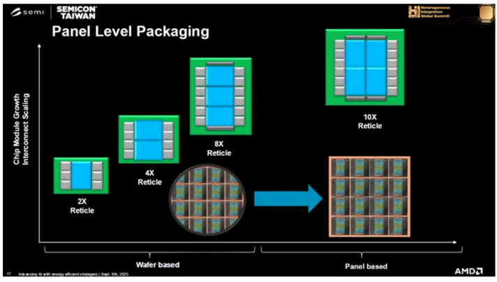
Source: AMD, Nomura research
The commercialization pathway to CoWoP is much longer without guarantee of success, although an even larger chip package could galvanize handler refreshes We delved into nVidia's innovative 'chip-on-wafer-on-PCB (CoWoP)' in our Asia AI Semi & Server Anchor Report in August 2025 , explaining that the CoW module is directly mounted onto a substrate-like PCB (SLP), which thereby eliminates the ABF substrate between the CoW module and high-density interconnect (HDI) PCB in the current configuration (Fig. 199 ). Switching from an IC substrate to an HDI PCB will essentially enlarge the package footprint and hence could galvanize new ATC/handler purchases for new mechanical designs (e.g. the shift to mega trays) and more challenging thermal requirements which are clearly a boon to Hon's equipment sales. Although we think SLP makers such as Unimicron (3037 TT, Buy) and Zhen Ding (4958 TT, Buy; Avary [002938 CH, Not rated] is its subsidiary) will continue to stay involved in the development given their past records of supplying to iPhone mainboards from 2017, ensuring low warpage and decent flatness when manufacturing CoWoP SLP, which is much larger and thicker than iPhone SLP, could be very challenging, and new materials might be considered.
In addition, as IC substrates bridge the line/space (L/S) differential between chips and PCBs, the removal of IC substrates might need extra RDLs build-up underneath CoW interposers. The bump pitch matching and coefficient of thermal expansion (CTE) matching between ICs and SLPs will be critical for CoWoP, and it could take a long time to resolve detailed technical issues.
We thus believe this project might remain in the R&D stage for the upcoming Rubin Ultra and Feynman. We will closely monitor the progress of this project, and would not be surprised if nVidia makes changes to adapt to real-world challenges.
Current CoWoS with
PCB
Fig. 199: CoWoP replaces ABF substrate + HDI PCB with SLP
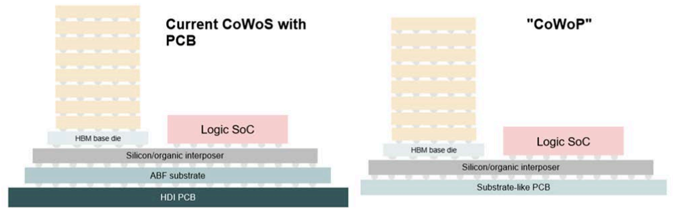
Source: Nomura research
Emerging OSATs' 2.5D engagements bode well for Hon, too
We render that more 2.5D/CoW engagements and capacity additions by OSATs could be a production driver for Hon's handler business, aside from TSMC's expansion. We first wrote about TSMC's prudent approach to CoW capacity expansion in our Asia AI Semi & Server Anchor report in August 2025 , and noted that such planning was critical for OSATs as it had driven most AI chip customers to look for alternative CoW suppliers. We estimate ASE (3711 TT, Buy) could form 25kwpm of FOCoS capacity by end-2026F, from 5kwpm installed by end-2025.
Amkor (AMKR US, Not rated) is also an alternate CoW partner, and management has highlighted over a dozen 2.5D engagements (silicon interposer-based, as per Amkor's definition) and expected high-density fan-out RDL devices (i.e., organic interposer-based) ramping up production in 2026E and bridge-type solution for AMD in 2027E (see Amkor's Investor Day 2026 ). Our industry checks suggest Amkor might have a c.15kwpm of 2.5D/SWIFT capacity by end-2026F.
Despite many 2.5D/molded interposer-based packages in the pipeline of OSATs are for CPUs owing to more relaxed technological requirements (e.g., RDL line/space) and the absence of expensive HBM content (report ), these chip packages are naturally more complicated than conventional FCBGA and could prolong the testing time. We elaborate about CPU opportunities in the subsequent section.
Fig. 200: 2.5D advanced packaging solution comparison
| 2.5D chip-last | TSMC | Intel Foundry | Samsung Foundry | ASE | SPIL | Amkor | Powertech |
|---|---|---|---|---|---|---|---|
| Silicon/TSV interposer | CoWoS-S (~3.3x ret.) | Foveros-S (~4x ret.) | I-CubeS H-Cube | 2.5D | 2.5D | 2.5D | 2.5D |
| Fan-out RDL | CoWoS-R (~5.5x ret.) | Foveros-R (production in 2027E) | n.a. | FOCoS | FO-MCM | S-SWIFT | CLIP (PLP) |
| Fan-out bridge (embedded in RDL) | CoWoS-L (>14x ret. by 2029E) | Foveros-B (production in 2027E) | I-CubeE | FOCoS-B | FO-EB | S-Connect | PiFO (PLP) (~9x ret. by 2028E) |
| Fan-out bridge (embedded in IC substrate) | - | EMIB (>12x ret. by 2028E) | - | - | - | - | - |
Source: Company data, Nomura research
Fig. 201: Major CoW projects at OSATs
| Fan-out RDL | Fan-out bridge | |
|---|---|---|
| ASE/SPIL | AMD Medusa? | AMD Venice |
| Amkor | nVidia GB10 nVidia Vera Microsoft Cobalt 200 | AMD Venice? (2027E) |
| Powertech | AMD Medusa? (PLP) | AMD's next gen? (PLP) |
Source: Company data, Nomura research
Hon to benefit from increasing testing spending by AI OSATs
We expect Hon's ATC/handler business to benefit from an increase in testing capex by AI OSATs as large package footprints remain the pillar of AI accelerators, and OSATs are aggressively adding floor space and tester capacity in response to the exponential surge in
"CoWop"
120
12,500
100
10,000
80
7,500
60
5,000
40
20
2,500
0
0
10
25
120
total test time per devices. We compile the capex plans and estimates of major OSATs with testing service exposure to North American AI chip customers, which appear poised to grow significantly in 2026-27E. Although some of them do not break down spending budgets to the assembly and testing stage, directionally we expect higher dollar spend on testing, with potential upside, contemplating TSMC's more aggressive CoWoS expansion plans and OSATs' participation in the full 2.5D turnkey. Meanwhile, SEMI also projects global test equipment spending to record a c.20% CAGR over 2025-28E. We believe all these factors indicate a robust ATC/handler growth trend for Hon through 2028F. For its near-term trajectory, we compare Hon's equipment set revenue patterns to leading-edge SoC tester TAM projections provided by Advantest and Teradyne as well, in view of the 1-for-1 relationship between tester sales and ATC/handler sales, which both imply robust y-y growth for Hon's equipment business.
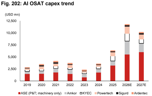
Source: Company data, Bloomberg Finance LP, Nomura estimates
Fig. 204: Hon's equipment set revenue vs. SoC tester estimates by Advantest
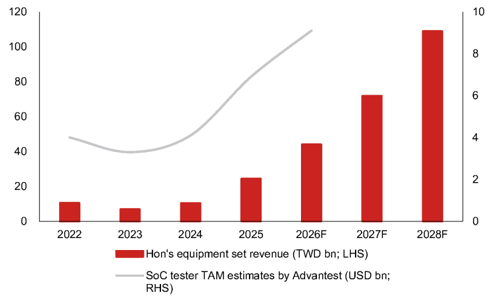
Source: Company data, Nomura estimates
2025
2026F
2027F
2028F
2023 2024 2025 2026E 2027E 2028E
- Growth rate y-y (RHS)
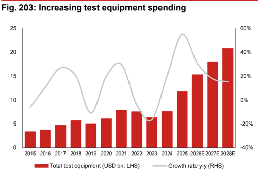
Source: SEMI, Nomura research
Fig. 205: Hon's equipment set revenue vs. SoC tester TAM estimates by Teradyne
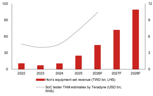
Note: Teradyne has not yet broken down ATE TAM of USD12-14bn in 2026E. We assume 80% of TAM goes to SoC testers based on historical patterns.
Source: Company data, Nomura estimates
Hon likely records more progress in SLT handlers
Hon historically focused the vast majority of its business engagements on FT handlers (7080% handler revenue comes from FT), but traditional ATE-driven FT alone may be no longer sufficient to detect all structural and functional defects since logic chip packages become more complicated. Hon has been making inroads into the SLT handler market by leveraging its competency in customization and ATC, and we believe a US CPU/GPU customer is one of its longstanding customers in SLT handlers.
We are aware that Hon has started an engineering collaboration with a US AI GPU vendor in SLT handlers for future-generation AI GPUs, and yet we have not factored this into our earnings estimates given the uncertainty of success; the segment is currently dominated by Chroma (2360 TT, Buy). In our view, Hon's new SLT handler opportunities could lie
2022
40%
9
20%
6
3
-20%
0
-40%
squarely within ASIC customers whose broader adoptions of SLT on top of mandatory FT has ballooned.
Mobile APs and CPUs also undergo architectural changes
We believe Hon could monetize the rising design complexity in certain mobile APs and CPUs due to the shift from a monolithic to a multi-die layout, and advanced packaging adoption originally pioneered in the AI/HPC space. The architectural changes could prolong testing time and therefore are clear positives to tester and handler purchases/upgrades. Meanwhile, chip performance boosts may drive additional ATC demand for more precise temperature control during the testing stage. Despite Hon's relatively small revenue contribution from mobile communication (10% of tool orders in 2025), our supply chain checks suggest Hon has a very strong foothold in FT handlers in mobile APs, supporting flagship mobile AP customers' products, and some high-end devices need air-cooling ATC as well.
Apple's WMCM and SoIC-MH could foster Hon's ATC/handler sales, and its packaging innovation endeavor is worth monitoring
We assume Apple's AP demand would remain strong despite declining Android units ( report ) and more importantly, Apple's upcoming A20 Pro package shift to wafer-level multi-chip module (WMCM; report ) will likely be the spotlight of ATC/handler upgrades in the mobile communication vertical in 2026F. We believe Hon will be the FT handler supplier for WMCM-based AP, to pair with the tester from Teradyne, and the test handler will require an ATC capable of thermal management up to 3,000W, vs. no ATC setup for the current InFO-PoP test handler. The ATC capability, in our view, could be more than sufficient to resolve potential self-heating issue of DUT, given that AP TDP usually ranges within 10-15W. We project ~50% boost to WMCM handler set ASP vs. InFO-PoP.
WMCM is a chip-last (RDL-first) fan-out scheme, which is comparable to TSMC's CoWoS-R process (yet without substrates), and RDL-first enables build-up of more RDLs at finer line/space (L/S) than InFO and therefore ensures better chip performance. We expect the WMCM process to shrink RDL L/S of A20 Pro to 5/5um, compared with InFOPoP at 10/10um, with identical three layers of RDL (Fig. 206 ). In the July 2025 report , we believed Apple would not grow its RDL layer count in A20 Pro likely because: 1) consumer applications do not require as many RDL layers as AI/HPC applications, whose layer count is typically more than five; or 2) Apple might utilize A20 Pro/WMCM as an experimental platform for potential future changes in packaging architecture.
As discussed in the 'Global Advanced Packaging - The evolution of CoWoS, SoIC and InFO ' report, our supply chain analysis suggests Apple has been likely working on a few hybrid bonding/SoIC projects for M-series silicon. Apple debuted M5 Pro and M5 Max in March 2026 (press ), and we witness that Apple disaggregates CPU and GPU blocks in the previous monolithic die into discrete sub-dies, and TSMC uses SoIC-MH to bond CPU and GPU chiplets onto a passive interposer using bump-less face-to-face hybrid bonding ( Fig. 207 ). While the SoIC-MH architecture is somewhat similar to 2.5D CoW, the M5 Pro/M5 Max can achieve substantially higher die-to-die interconnect density by replacing micro-bumps (2.5D CoW) with bump-less hybrid bonding, and reduce the parasitic losses (or 'chiplet tax') in chiplet-based layout.
We reason the shift to disaggregated die design could spark more stringent requirement for multi-zone thermal control during the testing stage, and thus the test equipment maker could enjoy a potential upgrade to ATC/hander. Furthermore, we believe it is worth monitoring the supply chain dynamics about whether Apple could bring SoIC in junction with WMCM (possibly with more RDL layers) to its M-series (or even mobile APs) beyond 2027F, given Apple's endeavor to foster chip packaging innovations at TSMC. More complicated, powerful silicons are apparently tailwinds to the backend testing supply chain including Hon's ATC/handlers.
Illustration
Mass production
RDL fabrication
RDL layers
RDL line/space (um)
Good die per wafer
Source: Company data, Nomura estimates
DRAM
WMCM
DRAM
Logic
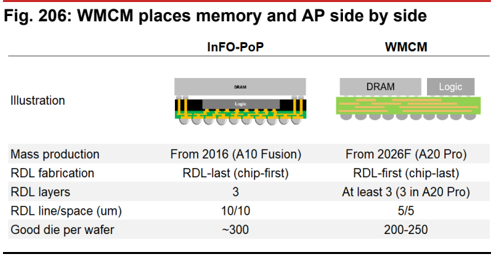
Source: Company data, Nomura estimates
M5 Max
Fusion Architecture introduced in 2026 M5 Pro and M5 Max laptops
Hybrid bonding of separate CPU and GPU chips to Si base die to form
Fig. 207: A cross section of SoIC-MH in Apple M5 Pro and M5 Max
LPDDR
GPU LPDDR
- CPU 4— Top die + Hybrid bond
LPDDR
Source: TechSearch International
• Hybrid bonding combines a common CPU chiplet with different GPU
chiplets (e.g. Pro and Max)
• Reduces die cost and increases yield by dividing chip design into 2
smaller chips
4 Base die
Source: TechSearch International
Source: Besi, TechSearch International, Nomura research
CPU testing growth recipe - higher volume meets more complexity
There have been growing discussions about server CPUs since 2H25 thanks to agentic AI, including insufficient supply as well as a crowd-out effect on client CPU production. Server CPU covers plain CPU for non-AI general servers, head-node CPUs paired with accelerators, and CPUs used for AI workloads (but not with accelerators). We believe the second and third categories are driving substantial demand for server CPUs, especially the last one after the agentic AI boom. Notably, AMD in May 2026 doubled its server CPU TAM forecast from USD60bn (provided in November 2024) to USD120bn+ by 2030E. We think Hon's handlers could ride on a stronger CPU demand volume, as it has been the primary handler vendor to support a US CPU customer.
We also observe changes in server CPU floor plans which could bring structural tailwinds to backend testing and Hon's handler sales, in our view. nVidia and some ARM-based CPUs by CSPs are moving from monolithic designs to multi-die or chiplets and possibly utilizing more advanced packaging technologies to facilitate faster die-to-die interconnects, such as molded interposers by TSMC's CoWoS-R and Amkor's S-SWIFT. nVidia's CEO Jensen Huang at the COMPUTEX keynote speech this year also spent more time on Vera CPUs and mentioned that 'Agent is a new workload. We built CPUs for humans in the past. We need CPUs for agents, agentic systems. The properties are different - why would the old CPUs be the same? ' . See our Asia AI Semi & Server Anchor Report for more details about CPU architecture revolutions.
nVidia's Vera CPU packages one compute die, one I/O die and four memory interface chiplets on a 2.2x reticle-sized organic interposer. nVidia emphasizes all 88 Olympus compute cores are in one monolithic compute mesh without 'chiplet tax' in core-to-core communication, and builds separate dies for memory controllers and I/Os to maximize the compute die area utilization for compute purposes. We think the chip design philosophy to offload memory controller blocks from the core compute complex may eventually become a common practice by ARM-based CPU designers and even AI accelerators (e.g., TPU v9 has independent memory fabrics, in our view; MediaTek has publicly illustrated such a concept, Fig. 208 ) to leave the precious die area to core compute.
We also flagged demand upside from Google's ARM-based CPU 'Axion N4A' (on TSMC 3nm; codenamed 'Cypress') to the Asia supply chain in August and December last year, which was in part driven by the CPU adoption shift in TPU 8t/8i from x86-based to Google Axion. We believe the supply chain logistics of Axion N4A are handled by GUC (3443 TT, Neutral), and KYEC (2449 TT, Buy) supports the FT stage using Advantest's ATE paired with Hon's ATC/handler, as well as the SLT stage using Chroma's handler. The current project in production has a monolithic layout, but our industry checks suggest the next generation may be a dual-die configuration, still utilizing FCBGA package, for releases in 2028F.
Admittedly, those changes in CPU layouts may not stipulate very large substrate sizes to foster transitions to mega trays and handler mechanical refreshes, but we argue that
nVidia
I/O
AMD
AWS
Microsoft
Arm chiplet-based or multi-die floor plans will trade monolithic simplicity for a highly complex testing paradigm to validate die-to-die interconnect efficiency at a longer testing time. Moreover, the multi-die layout naturally distributes the thermal load across the package and hence poses an intricate thermal management challenge to the ATC. The system must deploy ultra-precise, multi-zone active thermal heads to dynamically balance the wildly mismatched self-heating conditions across dies to prevent inflicting thermal damages on the chip package. Hon, in our view, possesses one-of-a-kind ATC capabilities to stand out as early in the engineering phases.
Fig. 208: Offloading memory controller interface blocks to chiplets
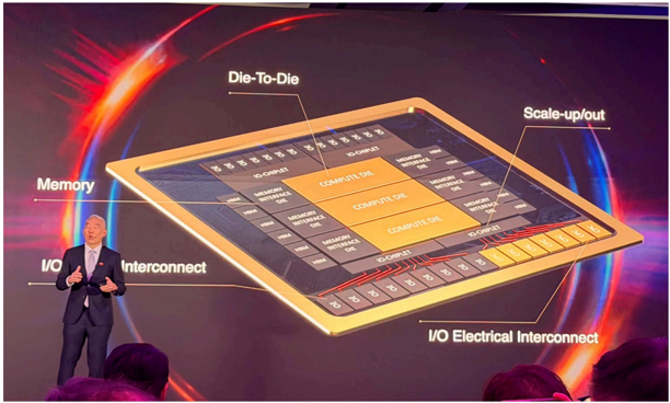
Source: MediaTek, Nomura research
?
?
AGI 3
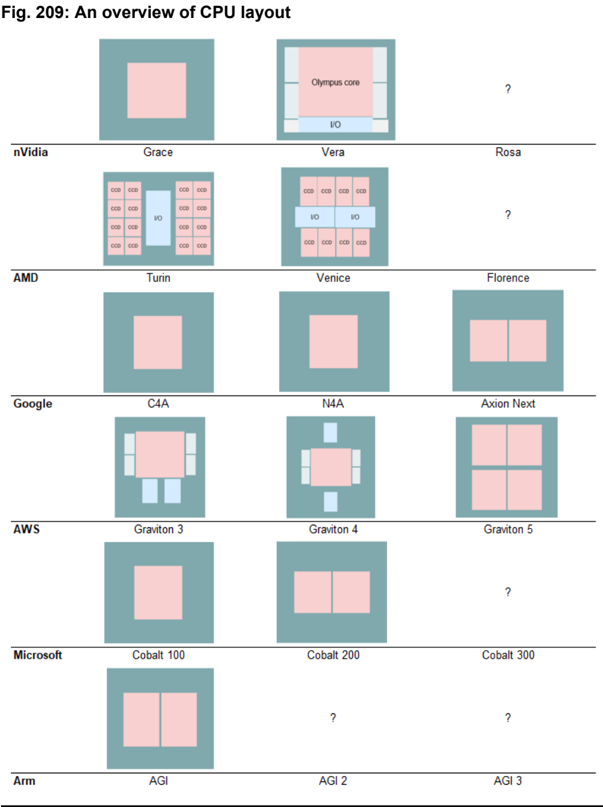
Source: Company data, Nomura estimates
Service flexibility and a well-extended thermal control roadmap to trump competition
We believe Hon's ATC/handlers can stand out among both regional and global peers in particularly high-power AI/HPC applications, due to: 1) unmatched customization; 2) pioneering ATC know-how; and 3) proximate flexibility in servicing the semiconductor backend cluster in Taiwan . The adjacency to the completed semiconductor ecosystem in Taiwan and more timely field engineering than overseas counterparts is an advantage shared by most Taiwan-based equipment makers, in our view. While IC test handlers alone might initially seem like simple mechanical automation which is often oversimplified as mere robotic arms picking and placing devices under test, the reality under the hood is a sophisticated combination of high-precision micromechanics and solid knowledge in thermal physics.
Theoretically the tier-one ATE maker Advantest could have enjoyed a natural installed base advantage in test handlers sales since handlers are used along with tester, and Advantest has advanced technological capabilities in mechatronics to optimize the coordination of handlers and testers. This is particularly valid in memory testing, where the testing relies on extreme parallelism (i.e. high throughputs on fairly standardized interfaces). Advantest was able to build up a large handler market share in the past when it leveraged its memory tester installed base, before it gradually lost ground to emerging memory handler specialists like Techwing (089030 KS, Not rated).
Hon's ATC/handler business serves primarily logic semi (it only had 1-2% of tool orders from memory in 2025), where the inherent advantage of Advantest disappears entirely. Logic packages are of high varieties than commodity memory, featuring varying physical dimensions, ball counts/pitches, etc., and this requires deep, early-stage collaboration during the new product introduction (NPI) phase as well as close-knit communication with specialized test interfaces (load boards and sockets) to build bespoke mechanics inside handlers. Specialized handler makers such as Hon can thrive on engineering fluidity. By contrast, Advantest does not devote many resources to tailor handlers given that handlers are essentially 'sidekicks' (1-2% of total revenue) and IC testers are its core business lines. This may also explain why Teradyne does not have its own handler business units given a great exposure to logic testing.
Handler customization is especially important and necessary in the realm of AI/HPC and ASICs due to large die sizes, complex multi-die packaging (e.g. 2.5D/CoWoS) and ultrahigh pin counts, and Hon is an expert in these areas (72% of tool orders from AI/HPC and ASICs in 2025). Hon engages directly into the embryonic development phases of AI/HPC and ASICs through tight NPI collaborations with end customers backed by a robust IP portfolio of more than 600 patents filed globally across thermal control, high-throughput, and active optical inspection (AOI), and ships early configurations to end customers' R&D labs for engineering validation and joint developments. We summarize Hon's NPI status (data as of 2Q25) in Fig. 210 .
Furthermore, the handler is more than a sheer mechanical sorter in AI/HPC testing as the accompanying ATC becomes an active execution environment. Hon's dual-temp and tritemp ATC cover a broad spectrum of operating temperatures and cooling systems (liquidcooling, refrigerant-cooling, and air-cooling), and the company continues to move forward in capabilities with an extended roadmap to 7,000-8,000W readiness and >10kW in the engineering pipeline (Fig. 192 ). A clear visibility of ATC roadmap and well execution, in our view, puts Hon in a more favorable position for AI/HPC clients looking to initiate new chip development.
20
15
10
5
0
Fig. 210: Hon's NPI status by application and end-customer location
US
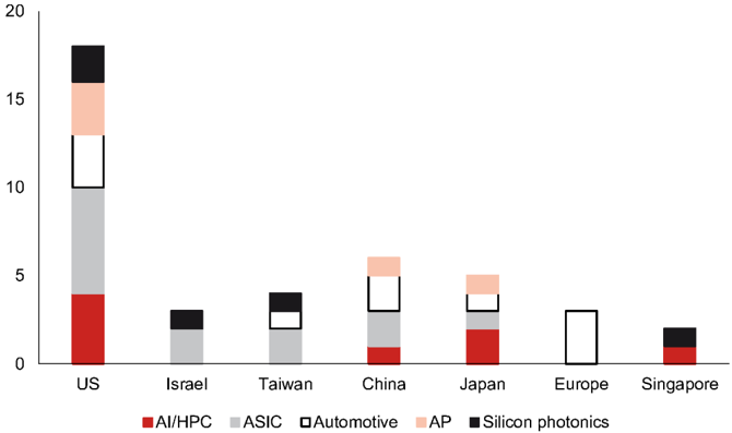
Note: Data as of 2Q25.
Source: Company data, Nomura research
Fig. 211: Comparison of major global tester and handler makers (ex-China)
| USD mn | Headquarter | Market cap | 2025 revenue | Revenue mix | Revenue mix | 2025 GM | 2025 OPM | 2025 net profit Tester | 2025 net profit Tester | Handler |
|---|---|---|---|---|---|---|---|---|---|---|
| USD mn | Headquarter | Market cap | 2025 revenue | Tester | Handler | 2025 GM | 2025 OPM | Handler | ||
| Hon. Precision (7769 TT) | Taiwan | 33,781.0 | 971.3 | n.a. | c.80% | 56.5% | 49.7% | 396.6 | n.a. | FT 70-80%, SLT 20-30% Mostly logic/analog |
| Chroma ATE (2360 TT) | Taiwan | 24,332.8 | 908.4 | 10-15% | 20-25% | 61.5% | 32.5% | 375.2 | Mature logic/analog | FT 30-40%, SLT 60-70% Mostly logic/analog |
| Advantest (6857 JP) | Japan | 123,945.2 | 6,902.1 | 82% | <5% | 62.4% | 39.7% | 1,927.8 | 80% Logic/Analog 20% Memory | FT, SLT Mostly memory |
| Kanematsu (8020 JP) | Japan | 2,157.8 | 7,062.3 | n.a. | <5% | 15.7% | 4.4% | 215.8 | n.a. | FT, SLT (from Seiko Epson) Mostly logic/analog |
| TESEC (6337 JP) | Japan | 75.5 | 37.6 | 45% | 36% | 37.8% | 5.7% | 2.0 | Mature logic/analog Discrete | FT (from Yokogawa) Mostly logic/analog |
| Cohu (COHU US) | US | 2,414.9 | 453.0 | ~40% | ~40% | 43.3% | 0.5% | (10.1) | Mature logic/analog | FT, SLT Mostly logic/analog |
| Teradyne (TER US) | US | 50,462.1 | 3,190 | 75% | 15% | 58.3% | 22.3% | 632.1 | 80% Logic/Analog 20% Memory | SLT Mostly logic/analog |
| Techwing (089030 KS) | South Korea | 1,222.7 | 112.0 | n.a. | 36% | 42.2% | 10.0% | 6.6 | n.a. | FT Mostly memory |
| SEMES (unlisted) | South Korea | n.a. | n.a. | n.a. | n.a. | n.a. | n.a. | n.a. | FT Mostly memory | |
| AEM (AEM SP) | Singapore | 2,137.2 | 305.6 | 30% | 30% | 25.7% | 5.9% | 13.0 | Mature logic/analog | FT, SLT Mostly logic |
Note: Market cap data as of July 17, 2026
Source: Company data, Bloomberg Finance LP, Nomura estimates
Hon is not absent from the manufacturing reshoring trend
We reason that Hon has strategically positioned itself in the semiconductor reshoring trend thanks to an extension of subsidiary network to the US in 2022, and to Germany in 2025 to close geographical gap and enhance service efficiency and localized supports. While the company's core equipment manufacturing hubs remain heavily anchored in Greater China to maximize production efficiency, these overseas subsidiaries could be vital beachheads for future expansions aligned to customer requests.
The global semiconductor manufacturing supply chain is undergoing a structural reshuffle owing to chip vendors' diversification needs in tandem with their home countries' government incentives. For instance, the US government has exerted aggressive industrial regimes including the CHIPS and Science Act and tariff pressures to rebuild (or replicate, to some extent) the domestic hardware ecosystem. American companies such as Apple and nVidia have touted homegrown supply programs (news and news ).
Arizona Advanced Packaging
Hon's US subsidiary is located in Austin, Texas, thereby placing itself amidst one of the burgeoning silicon clusters in the US, in our view, since a few American advanced chip designers like AMD and Tesla (TSLA US, Not rated) have campuses there. In Germany, we note that Hon's presence is to target distinct demand profiles and focus on the automotive and MEMS chip testing sectors in Europe. Positioning for future growth: secured additional 67 acres in May 2026
As Hon derives >50% of revenue from US end-customers, we think the most critical reshoring movements are TSMC's (advanced logic fabrication/packaging) and Amkor's (advanced packaging) expansion plans in Arizona, US, and KYEC's recent decision to build a factory in the US (news ). TSMC's plan, as of March 2025, was to build an advanced logic semiconductor production cluster with six wafer fabs and two advanced packaging facilities (press release ). The company recently unveiled plan to invest an additional USD100bn in Arizona (report ). According to TSMC, it has already started N4 mass production at Phase 1 and plans to move in tools in 2H26E at Phase 2 for N3 volume production in 2H27E; it has also started Phase 3 fab build (for N2) and will start the construction of wafer fab Phase 4 and an advanced packaging factory (AP1) this year (Fig. 212 ). As for Amkor, the company looks to invest USD7bn in an advanced packaging greenfield factory in Arizona, close to TSMC's fabrication complex, with high-volume manufacturing for the first phase slated to begin in 2028E and reach full-scale build-out by 2030E (Fig. 213 ).
Additionally, TSMC and Amkor have announced a long-term partnership in advanced backend services in the US (news and news ) likely because end-to-end regional supply would require coordination of wafer fabs and advanced packaging and test. Our current assumption is that TSMC might tilt the majority of new advanced logic capacity toward more lucrative AI/HPC silicon production, and advanced packaging capacity to CoW (rather than the full CoWoS turnkey) to better justify a more hefty outlay compared to investments in Taiwan, and Amkor's new site thus would shoulder more burden on WoS assembly and share backend testing workloads with KYEC. When TSMC, Amkor and KYEC start to tool the new sites and ramp up production, likely from 2028F, we expect Hon to benefit from another wave of machinery spending. We also believe Hon might have been mulling over potential factory setup in the US, likely for final tool assembly, while leaving the module production in Taiwan.
Fig. 212: TSMC is investing in the US
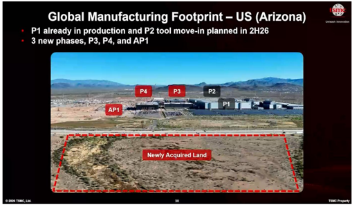
Source: TSMC, Nomura research
Fig. 213: Amkor is also building a backend megasite in the US
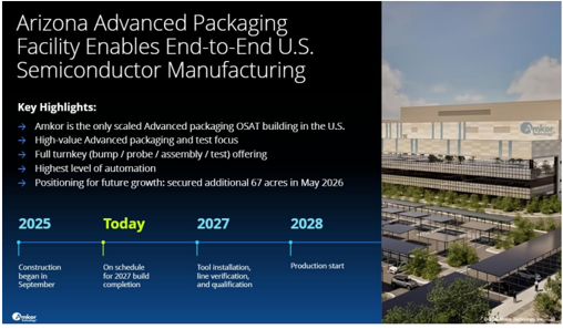
Source: Amkor, Nomura research
2028
Production start
Fig. 214: Hon's global footprint enable localized support, and Hon might be mulling over potential factory setup in the US
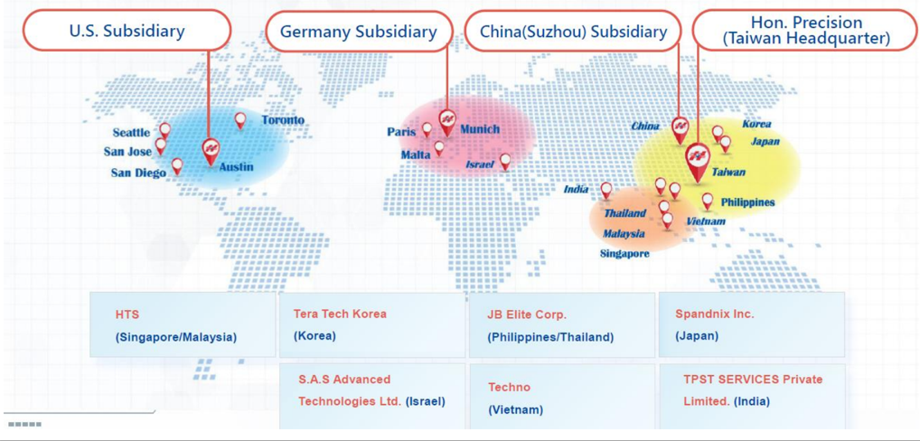
Source: Company data, Nomura research
Hon has a dominant position in high-end China AI and automotive testing
Hon derives about 20% of revenue from China, where the company focuses on AI/HPC and automotive verticals given more rigorous thermal control requirements during the test phase. Indigenous handler suppliers in China are mainly Changchuan (300604 CH, Not rated) and JHT (603061 CH, Not rated). We believe Hon's test handlers have a strong foothold in high-end Chinese AI/HPC and automotive chips, thanks to its superior temperature control capabilities at extremely high/low temperature (up to 170°C/down to -70°C) and greater cooling capacity (potentially up to 7,000-8,000W). China domestic counterparts' ATC are based on refrigerant-cooling or air-cooling and have not yet developed liquid-cooling ATC which are ideal for AI/HPC chip testing because of a faster heat transfer. We compare Hon, Changchuan, JHT, and other Chinese tester/handler vendors in Fig. 215 .
Hon's ATC/handlers are well positioned to capitalize on China's efforts to foster domestic AI/HPC silicon, in our view. China has shifted toward 2.5D advanced packaging, which aggregates more mature silicons to achieve target computing performance, to bypass tightening US curbs on its procurement of advanced wafer fabrication equipment. JCET (600584 CH, Buy) and SJ Semi (688820 CH, Not rated) are both very aggressive with 2.5D capacity expansion. As such, the testing complexity could skyrocket and unsanctioned backend testing equipment suppliers should be the beneficiaries, in our view.
30,000
25,000
20,000
15,000
10,000
5,000
0
Fig. 215: Comparison of Hon and Chinese indigenous tester and handler makers
| USD mn | Hon. Precision (7769 TT) | Changchuan (300604 CH) | Accotest (688200 CH) | JHT (603061 CH) | Powertech (301369 CH) |
|---|---|---|---|---|---|
| Headquarter | Taiwan | China | China | China | China |
| Market cap | 33,781.0 | 26,090.7 | 11,034.7 | 3,917.9 | 2,233.8 |
| 2025 revenue | 971.3 | 736.2 | 187.3 | 97.1 | 49.3 |
| Tester | n.a. | c.60% | c.90% | n.a. | c.85% |
| Handler | c.80% | c.30% | n.a. | c.90% | c.85% |
| 2025 GM | 56.5% | 55.1% | 73.8% | 52.2% | 55.7% |
| 2025 OPM | 49.7% | 24.4% | 36.5% | 30.5% | -3.1% |
| 2025 net profit | 396.6 | 185.2 | 74.6 | 24.6 | 4.7 |
| Tester | n.a. | n.a. | |||
| Application(s) | Logic/Analog Discrete | Logic/Analog Discrete | Logic/Analog Discrete | ||
| Handler | FT 70-80% SLT 20-30% | FT, SLT | n.a. | FT, SLT | FT |
| Application(s) | Mostly logic/analog | Logic/Analog Discrete | Logic/Analog Discrete | Logic/Analog Discrete |
Source: Company data, Bloonberg Finance LP, Nomura estimates
Fig. 216: China OSAT capex trend
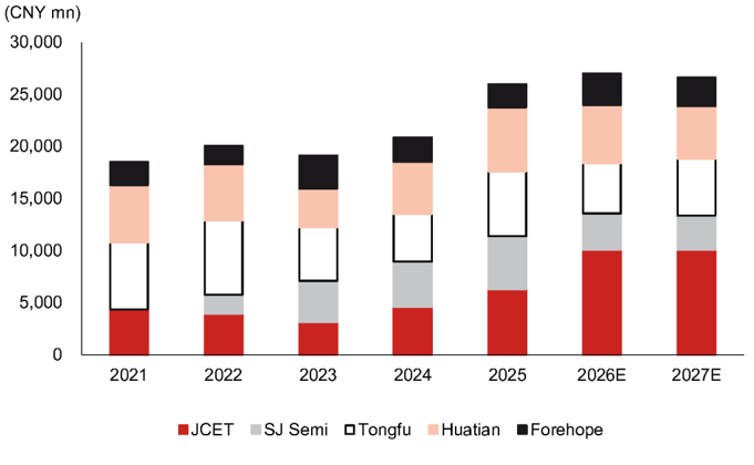
Source: Company data, Bloomberg Finance LP, Nomura research
The unsung hero of new technology deployments
We believe the role of semiconductor testing has also evolved into a foundational anchor that actively drives next-generation hardware architectures, in addition to a sheer postmanufacturing checkpoint, and Hon is poised to not only monetize the new technology adoption, but also steer the development. We see CPO and MCL emerging on the horizon, moving from R&D innovations to possibly support future chip-level/system-level interconnects and thermal dissipation respectively, but both will likely require an overhaul of current semiconductor backend test flows and simultaneously modifying and retrofitting testing tools (e.g., ATE and handlers). We think TSMC and its OSAT ecosystem partners have the incentives to raise investments in CPO and MCL from 2027F, in preparation for possibly broader adoption starting from Feynman in the earliest (scheduled fo 2H28E), and we thus expect Hon to ride on the spending wave with ASP upgrade tailwinds in 2027-28F.
New handler opportunity to start with CPO test insertion 4
We expect Hon's ATC/handlers to play a role in CPO testing, likely starting from test insertion 4 optical/electrical co-test (O/E co-test). O/E co-test is a multimodal test that simultaneously validates the optical and electrical properties of a CPO module housing switch ASIC and optical engines (OEs).
Any undetected defect in a single optical component would force manufacturers to scrap an entire expensive CPO switch module, and therefore testing cannot wait until final assembly. Strategically inserting tests early to validate known good optical/electrical dies and inspecting packages is the only way to manage the intense thermal-mechanical vulnerability of CPO and ensure viable manufacturing yield. As far as we are concerned, at the moment, there are four test insertions during TSMC and its ecosystem partners' CPO production, with two occurring under the scrutiny of TSMC and the subsequent two occurring at OSATs. See details of test insertions in our Anchor Report.
We think Hon could collaborate with ATE maker Teradyne in test insertion 4, with Teradyne's tester responsible for feeding electrical signals for testing; optical testing would be carried out by dedicated instruments (potentially by Keysight [KEYS US, Not rated]), in our view. Hon's handler will first facilitate optical alignment from an external laser source (ELS) to OE, via a receptacle or fiber array unit (FAU), and this process could be quite time-consuming and complicated. After setting up alignment, Hon's handler would enable the tester and instrument to test switch ASIC and OEs in one single touchdown. An ATC is also required in test insertion 4. Hon aims to complete the engineering verification by end-2026E and begin shipments in 2027E to address volume ramp-up in 2028E. Yet given fluid supply chain dynamics and uncertainty about CPO ramp-up timeline, we do not factor in contribution from CPO in detail. Any substantial progress could present an upside to our earnings forecasts beyond 2028F, in our view.
Hon's current business with CPO FT is electrical test only
We note that Hon has already shipped ATC/handlers for electrical tests (E/E test) of CPO switches in production (e.g., nVidia Spectrum-X and Quantum-X). The E/E test is executed on switch ASIC and OE together, or switch ASIC and OEs on a standalone basis.
Test Insertion
Insertion 1
Insertion 2
Fig. 217: CPO insertion flow
EIC
Test Content
HON. PREC
wafer-level test
Insertion 4
CPO FT
Mass Production
ASIC
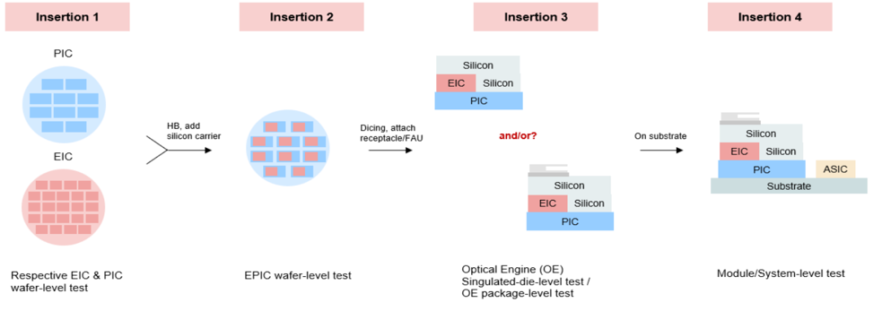
Respective EIC & PIC
Test Equipment
Note: This is a conceptual illustration, not specific to any company or project.
Source: Nomura research
Fig. 218: CPO insertion flow and potential suppliers
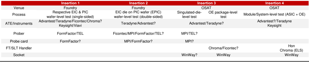
| Insertion 1 | Insertion 2 | Insertion 3 | Insertion 3 | Insertion 4 | |
|---|---|---|---|---|---|
| Venue | Foundry | Foundry | OSAT | OSAT | OSAT |
| Process | Respective EIC & PIC wafer-level test (single-sided) | EIC die on PIC wafer (EPIC) wafer-level test (double-sided) | Singulated-die- level test | OE package-level test | Module/System-level test (ASIC + OE) |
| ATE/Instruments | Advantest/Teradyne/Ficontec/Chroma? Keysight/Viavi | Teradyne/Advantest? | Advantest/Teradyne? | Advantest/Teradyne? | Advantest?/Teradyne Keysight |
| Prober | FormFactor/TEL | Ficontec/MPI/FormFactor/TEL? | MPI/TEL? | ||
| Probe card | FormFactor? | MPI/FormFactor? | MPI? | ||
| FT/SLT Handler | Chroma/Ficontec? | Hon Chroma (ELS) | |||
| Socket | WinWay? | WinWay | WinWay |
Source: Nomura research
Fig. 219: Hon's role in CPO test insertions
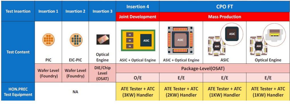
Source: Company data, Nomura research
Insertion 2
Insertion 3
Insertion 4
Joint Development
Silicon
EIC Silicon
PIC
Insertion 3
Test Insertion
Fig. 220: How CPO switches are tested in the current CPO FT vs. CPO test insertion 4
ASIC
ASIC
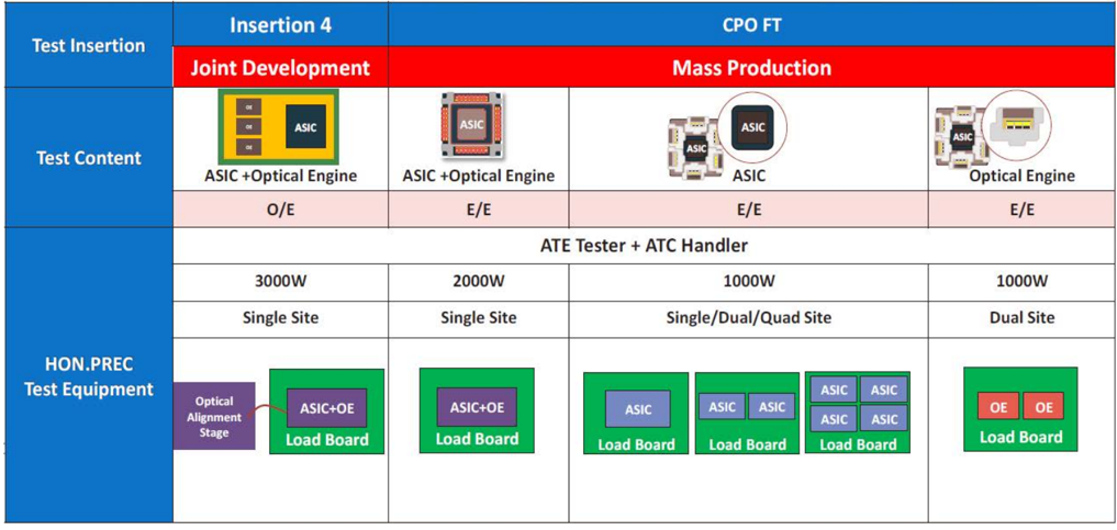
Test Content
HON.PREC
Test Equipment
Source: Company data, Nomura research
MCL may require changes to ATC/handler and testing flows
We think the thermal challenges arising from Feynman's first-ever GPU-on-GPU SoIC stacking could again spark industry evaluation and discussion of MCL adoption as the structure may drive chip TDP easily above 3,000W, and more importantly, a sharp leap in power density/heat flux on fairly limited expansion in interposer/substrate size. We believe there would be significant coordination of workflows and clarification of responsibilities as the supply chain reshuffles and prepares for MCL, and Hon could largely lead in technological breakthrough. We believe a dedicated new handler is a must for MCLbased packages, and Hon could have the tool platform ready in 4Q26F at the earliest.
Currently, liquid cooling cold plates are placed on heat spreaders, with a layer of TIM2 in between. Liquid coolant traverses through the channels on cold plates and removes heat from the processors underneath. The convective heat transfer coefficient is the predominant factor of liquid cooling performance, directly correlated to the fluid flow rate and inversely correlated to channel pitch. Nevertheless, higher flow rates or narrow channel dimensions come at the cost of higher pressure drop between the liquid inlet and outlet, which could consume more energy to pump the coolant.
An MCL integrates coolant channels on a cold plate into a lid cover or heat spreader ('microchannels') and eliminates the use of cold plate and TIM2 layer. The traditional heat dissipation path of 'Die→TIM1→Lid→TIM2→Cold Plate', is thus shortened to 'Die→ TIM1→MCL'. The elimination of the use of TIM2 and the boundary between heat spreader (lid) and cold plate can reduce thermal resistance and upgrade cooling performance (Fig. 221 ). The MCL use could be necessary, since the traditional singlephase liquid cooling cold plates could reach their heat dissipation limits when AI chip TDP approaches 3,000W. An extensive technology discussion of MCL and advanced cooling alternatives can be found in our October 2025 Asia AI Thermal Anchor Report .
Assembly of MCL on top of a chip package will likely be done by CoWoS makers (TSMC and its alliance). Currently, TSMC and its OSAT partners attach a heat spreader as the last step of CoWoS, and a cold plate is attached to the IC package by ODM and/or EMS providers. The heat sink/cold plate attachment equipment is subject to modification to fit in a new heat spreader design as well. The adoption of MCL could affect how chips are tested to ensure no coolant leakage after CoWoS assembly, and testing equipment might undergo reconfiguration for thermal controls and ensure no excess contact force exerted on the MCL leading to damage.
CPO FT
Fig. 221: MCL and its cross-section view
Thermal chip
PCB.
(a)
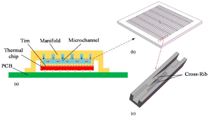
Source: Micromachines, Volume 13 (2022), Issue 1 'Evaluation and Optimization of a Cross-Rib Micro-Channel Heat Sink', Nomura research
Earnings forecasts and financial analysis
We expect a 70% net earnings CAGR over 2025-28F
After strong 116% y-y revenue growth in 2025 driven by a US AI GPU vendor's OSAT partner's testing ramp-up and capacity expansion to support strong demand for the AI GPU platform, we expect Hon's revenue to increase by 90% y-y in 2026F, since the Asia AI OSAT supply chain continues the capacity expansion for not only the US customer's AI GPU platform refresh, but also AI ASIC camp's strong ramp-up (notably a top US CSP). In addition, Apple's migration in chip package technologies (e.g. WMCM) adds to the strong momentum. We expect Hon's revenue to witness a 69% CAGR over 2025-28F given the structural testing trend of increased complexity and longer time and its endeavor to expand factory space.
We model Hon's equipment set shipments based on its productivity and loadings, and is aware of the company's plan to grow total factory floor space by 50% p.a. in the next few years (we estimate 40-45% equipment set capacity growth p.a.). We summarize Hon's current factory and upcoming plans in Fig. 237 . For equipment manufacturers, there is always lead time between equipment shipments and revenue recognition, given the need for tool installation, pilot runs and verifications, and Hon generally books revenue three to six months after tool shipments. We factor the two-quarter lag into our earnings model.
We note that Hon's equipment set sales include handler, ATC and cold plates in one set, and based on Hon's estimates, the current equipment set ASP comprises 42% from handlers, 33% from ATC and 23% from cold plates. We see fairly limited growth in handler ASP before the mechanical refresh advent steered by large-package handlers or MCL handlers. Most of the incremental ASP, in our view, will be underpinned by ATC upgrades in tandem with AI/HPC customers' chip roadmaps. We therefore project Hon's equipment set blended ASP will grow from TWD12mn in 2025F to TWD20mn in 2028F.
The initial equipment set opportunities from MCL and CPO test insertion 4 (albeit likely small) might kick in from late-2026F at the earliest, but we have not yet contemplated the detailed contribution of MCL or O/E co-testing in our earnings estimates as the supply chain dynamics remain fluid, and we have to continue monitoring the development and viability of new technologies.
On the profitability front, we project a rather stable GM profile across Hon's major product lines, and believe tool upgrades (notably ATC) are the predominant factors to the company's GM upswings. Our current assumptions consider a steady step-up in ASP to reflect continued ATC upgrades along with AI/HPC customers' roadmap primarily. Despite not in our estimates as yet, we believe MCL and CPO test insertion tools could be accretive to Hon's GM at a higher-than-average ASP. We, hence, model GM of 56.7%/56.9%/56.9% in 2026F/27F/28F, vs 56.5% in 2025.
Blending in a 60% opex CAGR over 2025-28F (we note that Hon expects 50% headcount growth in 2026E and continues to expand factory spaces), we anticipate Hon to enjoy operating leverage from rapid top-line expansion and grow its OPM to 51.1% in 2028F from 49.7% in 2025. In all, we estimate the company to deliver a 70% EPS CAGR over 2025-28F and are aware that a successful ramp-up of new technologies (MCL or CPO test insertion) into 2028F could drive a significant earnings upgrade.
We anticipate a stable cash conversion cycle (CCC) for Hon, and model Hon to dial up capex to TWD1.5bn/TWD2.4bn/TWD3.7bn in 2026F/27F/28F vs an average spending of TWD210mn a year during 2023-25, due to its intention to grow factory spaces. That said, we think Hon will keep its earnings payout ratio at ~70% in coming years.
160,000
140,000
120,000
100,000
80,000
60,000
40,000
20,000
0
Fig. 222: Hon's revenue trend
75,000
60,000
45,000
30,000
15,000
0
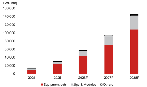
Source: Company data, Nomura estimates
Fig. 224: Hon - P&L
| (TWD mn) | 1Q25 | 2Q25 | 3Q25 | 4Q25 | 1Q26 | 2Q26F | 3Q26F | 4Q26F | 1Q27F | 2Q27F | 3Q27F | 4Q27F | 2025 | 2026F | 2027F | 2028F |
|---|---|---|---|---|---|---|---|---|---|---|---|---|---|---|---|---|
| Revenue | 5,913 | 6,885 | 8,198 | 9,276 | 10,725 | 13,794 | 15,582 | 17,305 | 19,459 | 22,377 | 25,098 | 27,361 | 30,271 | 57,406 | 94,295 | 145,102 |
| Gross profit | 3,494 | 4,037 | 4,730 | 4,852 | 6,032 | 7,834 | 8,860 | 9,846 | 11,074 | 12,729 | 14,282 | 15,586 | 17,114 | 32,571 | 53,671 | 82,492 |
| - Opex | (360) | (394) | (565) | (749) | (672) | (869) | (982) | (1,090) | (1,187) | (1,365) | (1,531) | (1,669) | (2,068) | (3,613) | (5,752) | (8,416) |
| Operating profit | 3,133 | 3,643 | 4,166 | 4,104 | 5,360 | 6,965 | 7,878 | 8,755 | 9,887 | 11,364 | 12,751 | 13,917 | 15,046 | 28,958 | 47,919 | 74,076 |
| Pretax profit | 3,235 | 3,156 | 4,524 | 4,669 | 5,798 | 7,236 | 8,183 | 9,028 | 10,182 | 11,688 | 13,113 | 14,236 | 15,584 | 30,245 | 49,219 | 75,703 |
| Net profit | 2,568 | 2,466 | 3,617 | 3,711 | 4,624 | 5,789 | 6,547 | 7,222 | 8,145 | 9,351 | 10,490 | 11,389 | 12,362 | 24,182 | 39,375 | 60,563 |
| EPS (TWD) | 15.89 | 15.26 | 22.39 | 22.13 | 25.70 | 32.18 | 36.39 | 40.14 | 45.28 | 51.98 | 58.31 | 63.31 | 75.71 | 134.42 | 218.87 | 336.64 |
| Profitability | 1Q25 | 2Q25 | 3Q25 | 4Q25 | 1Q26 | 2Q26F | 3Q26F | 4Q26F | 1Q27F | 2Q27F | 3Q27F | 4Q27F | 2025 | 2026F | 2027F | 2028F |
| Gross margin | 59.1% | 58.6% | 57.7% | 52.3% | 56.2% | 56.8% | 56.9% | 56.9% | 56.9% | 56.9% | 56.9% | 57.0% | 56.5% | 56.7% | 56.9% | 56.9% |
| - Opex ratio | -6.1% | -5.7% | -6.9% | -8.1% | -6.3% | -6.3% | -6.3% | -6.3% | -6.1% | -6.1% | -6.1% | -6.1% | -6.8% | -6.3% | -6.1% | -5.8% |
| Operating margin | 53.0% | 52.9% | 50.8% | 44.2% | 50.0% | 50.5% | 50.6% | 50.6% | 50.8% | 50.8% | 50.8% | 50.9% | 49.7% | 50.4% | 50.8% | 51.1% |
| Pretax margin | 54.7% | 45.8% | 55.2% | 50.3% | 54.1% | 52.5% | 52.5% | 52.2% | 52.3% | 52.2% | 52.2% | 52.0% | 51.5% | 52.7% | 52.2% | 52.2% |
| Net margin | 43.4% | 35.8% | 44.1% | 40.0% | 43.1% | 42.0% | 42.0% | 41.7% | 41.9% | 41.8% | 41.8% | 41.6% | 40.8% | 42.1% | 41.8% | 41.7% |
| Q-Q | 1Q25 | 2Q25 | 3Q25 | 4Q25 | 1Q26 | 2Q26F | 3Q26F | 4Q26F | 1Q27F | 2Q27F | 3Q27F | 4Q27F | ||||
| Revenue | 19.2% | 16.4% | 19.1% | 13.1% | 15.6% | 28.6% | 13.0% | 11.1% | 12.4% | 15.0% | 12.2% | 9.0% | ||||
| Gross profit | 30.2% | 15.6% | 17.2% | 2.6% | 24.3% | 29.9% | 13.1% | 11.1% | 12.5% | 15.0% | 12.2% | 9.1% | ||||
| Operating profit | 42.9% | 16.3% | 14.3% | -1.5% | 30.6% | 29.9% | 13.1% | 11.1% | 12.9% | 14.9% | 12.2% | 9.2% | ||||
| Pretax profit | 30.2% | -2.4% | 43.4% | 3.2% | 24.2% | 24.8% | 13.1% | 10.3% | 12.8% | 14.8% | 12.2% | 8.6% | ||||
| Net profit | 30.6% | -4.0% | 46.7% | 2.6% | 24.6% | 25.2% | 13.1% | 10.3% | 12.8% | 14.8% | 12.2% | 8.6% | ||||
| Y-Y | 1Q25 | 2Q25 | 3Q25 | 4Q25 | 1Q26 | 2Q26F | 3Q26F | 4Q26F | 1Q27F | 2Q27F | 3Q27F | 4Q27F | 2025 | 2026F | 2027F | 2028F |
| Revenue | 142.4% | 128.7% | 128.9% | 87.0% | 81.4% | 100.4% | 90.1% | 86.6% | 81.4% | 62.2% | 61.1% | 58.1% | 116.3% | 89.6% | 64.3% | 53.9% |
| Gross profit | 188.1% | 120.5% | 139.8% | 80.8% | 72.6% | 94.0% | 87.3% | 102.9% | 83.6% | 62.5% | 61.2% | 58.3% | 122.3% | 90.3% | 64.8% | 53.7% |
| Operating profit | 220.3% | 143.0% | 158.1% | 87.1% | 71.1% | 91.2% | 89.1% | 113.4% | 84.5% | 63.2% | 61.9% | 59.0% | 139.4% | 92.5% | 65.5% | 54.6% |
| Pretax profit | 183.3% | 102.7% | 201.9% | 87.8% | 79.2% | 129.3% | 80.9% | 93.4% | 75.6% | 61.5% | 60.2% | 57.7% | 133.2% | 94.1% | 62.7% | 53.8% |
| Net profit | 179.3% | 101.9% | 206.6% | 88.8% | 80.1% | 134.8% | 81.0% | 94.6% | 76.1% | 61.5% | 60.2% | 57.7% | 133.9% | 95.6% | 62.8% | 53.8% |
Source: Company data, Nomura estimates
Fig. 225: Hon's revenue breakdown by segment
| TWD mn | 2024 | 2025 | 2026F | 2027F | 2028F |
|---|---|---|---|---|---|
| Total revenue | 13,992 | 30,271 | 57,406 | 94,295 | 145,102 |
| y-y growth | 47% | 116% | 90% | 64% | 54% |
| Equipment sets | 10,226 | 24,371 | 43,869 | 71,682 | 108,810 |
| y-y growth | 51% | 138% | 80% | 63% | 52% |
| Jigs & Modules | 3,147 | 5,050 | 12,419 | 20,821 | 33,571 |
| y-y growth | 49% | 60% | 146% | 68% | 61% |
| Others | 619 | 850 | 1,118 | 1,792 | 2,720 |
| y-y growth | 2% | 37% | 32% | 60% | 52% |
Source: Company data, Nomura estimates
120%
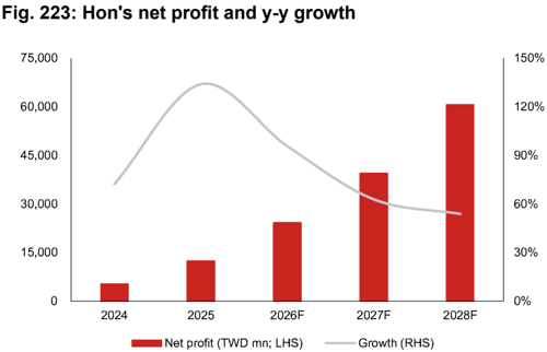
Source: Company data, Nomura estimates
Fig. 226: Nomura forecasts vs Bloomberg consensus for 2026-28F
| 2026F | 2026F | 2026F | 2027F | 2027F | 2027F | 2028F | 2028F | 2028F | |
|---|---|---|---|---|---|---|---|---|---|
| (TWD mn) | NMR | BBG | Diff. | NMR | BBG | Diff. | NMR | BBG | Diff. |
| Revenue | 57,406 | 52,876 | 8.6% | 94,295 | 83,446 | 13.0% | 145,102 | 139,035 | 4.4% |
| Gross profit | 32,571 | 30,057 | 8.4% | 53,671 | 48,357 | 11.0% | 82,492 | 82,952 | -0.6% |
| Operating profit | 28,958 | 26,484 | 9.3% | 47,919 | 42,938 | 11.6% | 74,076 | 70,682 | 4.8% |
| Pretax profit | 30,245 | 28,417 | 6.4% | 49,219 | 43,857 | 12.2% | 75,703 | 71,738 | 5.5% |
| Net profit | 24,182 | 21,558 | 12.2% | 39,375 | 34,138 | 15.3% | 60,563 | 56,673 | 6.9% |
| EPS (TWD) | 134.42 | 123.18 | 9.1% | 218.87 | 201.13 | 8.8% | 336.64 | 338.25 | -0.5% |
| Margin | NMR | BBG | Diff. | NMR | BBG | Diff. | NMR | BBG | Diff. |
| Gross margin | 56.7% | 56.8% | -11bps | 56.9% | 58.0% | -103bps | 56.9% | 59.7% | -281bps |
| Operating margin | 50.4% | 50.1% | 36bps | 50.8% | 51.5% | -64bps | 51.1% | 50.8% | 21bps |
| Pretax margin | 52.7% | 53.7% | -106bps | 52.2% | 52.6% | -36bps | 52.2% | 51.6% | 58bps |
| Net margin | 42.1% | 40.8% | 135bps | 41.8% | 40.9% | 85bps | 41.7% | 40.8% | 98bps |
Source: Bloomberg Finance L.P. consensus, Nomura estimates
60
50
40
30
20
10
0
Jul-25
25.0
Valuation methodology and risks
We derive our target price of TWD11,100 based on 40x average 2027-28F EPS of TWD278. Our target P/E multiple is at the high end of Hon's historical trading band of 1952x since its IPO, which we consider undemanding given a 58% net earnings CAGR through 2026-28F. We believe a structurally extended testing time for AI/HPC chips and more stringent thermal requirements during test will continue to drive Hon's revenue and earnings expansion, alongside the company's efforts to enlarge its production capacity. Although we do not factor in contribution from CPO test insertions or MCL in detail, a successful ramp-up of new technologies and associated testing approach changes could drive further upgrades to earnings estimates beyond 2028F.
Jan-26
We select Hon's peers from semiconductor backend equipment and test interface vendors for valuation comparison. Hon is currently trading at 29x 2027F EPS and 19x 2028F EPS, respectively, and we view this apparently very attractive compared to an average valuation level of 39x by semiconductor back-end testing equipment makers and 35x by test interface peers, all based on 2027E EPS.
Major downside risks to our call include: 1) CoWoS and back-end testing capacity expansion slowdown; 2) slower-than-expected product refresh, platform performance upgrade, or ramp-up by the AI chip end customers; 3) fiercer-than-expected market competition in test handlers; and 4) weaker-than-expected end-market demand, particularly for AI servers.
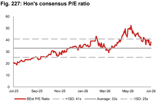
Source: Bloomberg Finance LP, Nomura research
Fig. 229: Semi test sector valuation comparison
| Last close | Target price | Upside (Downside) | Market Cap. | P/E | P/E | P/E | P/B (x) | P/B (x) | P/B (x) | ROE | ROE | ROE | Dividend yield | Dividend yield | Dividend yield | |||
|---|---|---|---|---|---|---|---|---|---|---|---|---|---|---|---|---|---|---|
| Ticker | Company Name | Rating | LCY | LCY | % | USD mn | FY26F | FY27F | FY28F | FY26F | FY27F | FY28F | FY26F | FY27F | FY28F | FY26F | FY27F | FY28F |
| Semi test equipment | ||||||||||||||||||
| 6857 JP | Advantest | Buy | 29,585.0 | 30,600.0 | 3 | 132,836 | 44.2 | 34.4 | 27.7 | 20.4 | 15.5 | 11.9 | 52.5% | 51.2% | 48.7% | 0.2% | 0.2% | 0.2% |
| TER US | Teradyne | Not rated | 374.0 | n.a. | n.a. | 58,553 | 51.1 | 37.2 | 26.7 | 16.2 | 13.1 | 10.0 | 37.5% | 41.7% | 41.9% | 0.1% | 0.1% | 0.2% |
| KEYS US | Keysight | Not rated | 328.1 | n.a. | n.a. | 56,072 | 32.2 | 27.6 | 24.6 | 8.2 | 6.8 | 5.6 | 25.9% | 26.4% | 26.1% | 0.0% | 0.0% | 0.0% |
| 7769 TT | Hon Precision | Buy | 6,405.0 | 11,100.0 | 73 | 35,597 | 47.7 | 29.3 | 19.0 | 16.3 | 12.4 | 9.1 | 37.6% | 48.1% | 55.3% | 1.5% | 2.4% | 3.7% |
| 300604 CH | Changchuan | Not rated | 309.1 | n.a. | n.a. | 28,944 | 94.5 | 64.3 | 46.8 | 29.3 | 20.5 | 14.5 | 33.4% | 34.7% | 33.7% | 0.1% | 0.2% | 0.2% |
| 2360 TT | Chroma | Buy | 2,125.0 | 2,845.0 | 34 | 27,912 | 48.7 | 32.4 | 25.2 | 21.3 | 15.7 | 12.3 | 49.8% | 55.8% | 54.6% | 1.4% | 2.2% | 2.8% |
| 688200 CH | Accotest | Not rated | 369.0 | n.a. | n.a. | 10,926 | 94.8 | 75.0 | 58.8 | 14.2 | 13.4 | 11.3 | 16.2% | 17.8% | 19.1% | 0.3% | 0.4% | 0.6% |
| COHU US | Cohu | Not rated | 56.2 | n.a. | n.a. | 2,652 | 95.8 | 38.3 | 26.4 | 3.5 | 3.2 | 2.9 | -207.6% | 27.2% | n.a. | n.a. | n.a. | n.a. |
| AEM SP | AEM | Not rated | 9.0 | n.a. | n.a. | 2,235 | 42.4 | 27.7 | 21.0 | 5.2 | 4.4 | 3.7 | 13.0% | 16.8% | 18.9% | 0.6% | 0.9% | 1.2% |
| 6337 JP | TESEC | Not rated | 2,339.0 | n.a. | n.a. | 80 | 20.3 | 18.8 | 16.3 | n.a. | n.a. | n.a. | n.a. | n.a. | n.a. | 4.3% | 4.3% | 4.3% |
| Average | 57.2 | 38.5 | 29.3 | 14.9 | 11.7 | 9.0 | ||||||||||||
| Semi test interface | ||||||||||||||||||
| TPRO IM | Technoprobe | Not rated | 31.2 | n.a. | n.a. | 22,854 | 71.9 | 47.2 | 37.0 | 13.2 | 10.5 | 8.3 | 19.6% | 22.6% | 23.1% | 0.0% | 0.1% | 0.2% |
| 6223 TT | MPI | Buy | 6,000.0 | 8,000.0 | 33 | 18,159 | 100.5 | 46.8 | 26.4 | 31.0 | 20.5 | 13.1 | 35.7% | 54.8% | 63.1% | 0.5% | 1.2% | 2.1% |
| FORM US | FormFactor | Not rated | 113.8 | n.a. | n.a. | 8,867 | 46.1 | 35.7 | 39.4 | n.a. | n.a. | n.a. | 15.4% | 18.7% | n.a. | 0.0% | 0.0% | n.a. |
| 6515 TT | WinWay | Buy | 6,500.0 | 8,315.0 | 28 | 7,235 | 73.6 | 35.0 | 19.5 | 32.7 | 20.6 | 12.8 | 46.4% | 71.6% | 80.4% | 1.0% | 2.2% | 3.9% |
| 6510 TT | CHPT | Suspended | 2,710.0 | n.a. | n.a. | 2,745 | 42.2 | 22.7 | 15.9 | 8.2 | 6.3 | n.a. | 20.8% | 31.8% | 56.0% | 1.3% | 2.3% | 2.9% |
| COHU US | Cohu | Not rated | 56.2 | n.a. | n.a. | 2,652 | 95.8 | 38.3 | 26.4 | 3.5 | 3.2 | 2.9 | -207.6% | 27.2% | n.a. | n.a. | n.a. | n.a. |
| 6941 JP | Yamaichi | Not rated | 9,380.0 | n.a. | n.a. | 1,181 | 17.6 | 15.7 | 13.7 | 3.2 | 2.8 | 2.4 | 19.3% | 20.4% | 20.7% | 1.7% | 1.8% | 2.1% |
| 6683 TT | KSMT | Not rated | 1,220.0 | n.a. | n.a. | 1,038 | n.a. | n.a. | n.a. | n.a. | n.a. | n.a. | n.a. | n.a. | n.a. | n.a. | n.a. | n.a. |
| Average | 64.0 | 34.5 | 25.5 | 15.3 | 10.6 | 7.9 | ||||||||||||
| AI OSAT | ||||||||||||||||||
| 3711 TT | ASE | Buy | 656.0 | 730.0 | 11 | 90,585 | 37.2 | 25.5 | 20.2 | 7.1 | 6.2 | 5.5 | 19.7% | 25.6% | 28.6% | 1.9% | 2.8% | 3.5% |
| AMKR US | Amkor | Not rated | 66.7 | n.a. | n.a. | 16,541 | 31.9 | 27.5 | 23.1 | 3.3 | 3.0 | 2.6 | 11.2% | 11.1% | 12.7% | 0.5% | 0.5% | 0.6% |
| 2449 TT | KYEC | Buy | 295.0 | 390.0 | 32 | 11,142 | 30.3 | 19.1 | 14.3 | 5.7 | 4.5 | 3.5 | 21.0% | 26.4% | 27.3% | 0.3% | 0.5% | 0.7% |
| 6239 TT | Powertech | Not rated | 294.0 | n.a. | n.a. | 6,894 | 24.5 | 16.9 | 15.0 | 3.4 | 3.0 | 2.7 | 15.7% | 18.8% | 18.6% | 2.4% | 3.3% | 3.7% |
| Average | 31.0 | 22.3 | 18.1 | 4.9 | 4.2 | 3.6 |
Note: Priced as of July 22, 2026.
Source: Company data, Bloomberg Finance L.P., Nomura estimates
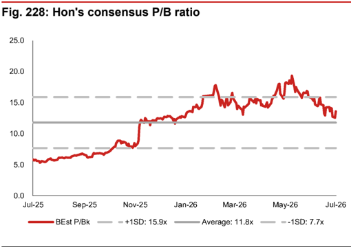
Source: Bloomberg Finance LP, Nomura research
Mar-26
Average: 11.8x
May-26
Jul-26
--1SD: 7.7x
9,100
8,100
9,000
8,000
7,100
6,100
5,100
7,000
4,100
3,100
6,000
5,000
2,100
1,100
100
4,000
Nov-24
3,000
2,000
1,000
0
Nov-24
9,000
8,000
7,000
5,000
Market sell-off and macro concerns (yields); market
concerns with delayed CPO
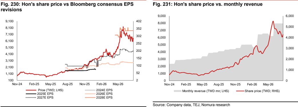
Source: Company data, Bloomberg Finance L.P. consensus estimates, Nomura research
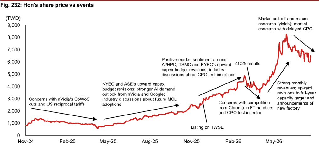
Source: Company data, TEJ, Nomura research
Source: Company data, TEJ, Nomura research
402
Company background
Headquartered in Taichung City, Taiwan, Hon. Technology was founded in 1999 and reincorporated to the current 'Hon. Precision (Hon)' in 2015. Hon is a dedicated semiconductor equipment manufacturer focusing on IC test handlers and active thermal control systems (ATC) for IC backend testing. Hon's client base spans across major IC design houses, outsourced semiconductor assembly and test vendors (OSATs), and integrated device manufacturers (IDMs) worldwide, and the company has also established a complete global service network via subsidiaries in China, the US, and Germany as well as agencies in Korea and Southeast Asia.
Hon's primary production bases are in Taichung City, Taiwan, and two sites in China. The company has been actively seeking new land or plants to further expand the equipment and jig/module capacity. Management expects more than 25% factory space expansion and more than 40% equipment set capacity growth in 2026E, with a preliminary target to enlarge factory space by 50% every year onwards.
Hon's IC test handlers and ATC are used in the final test (FT) or system level test (SLT) stage of semiconductor production, for GPUs, CPUs, and application processors (AP). Hon's handlers are primarily pick-and-place handlers, which uses suction to transfer the DUT and press it into the test sockets. In ATC, Hon offers both dual-temp (high temperature [up to 170°C] and ambient temperature [around 25°C]) and tri-temp (high temperature, ambient temperature, and low temperature [down to -70°C]) ATC capabilities, based on three types of cooling system - Liquid-cooling (ATC3 series), Refrigerant-cooling (ATC5 series), and Air-cooling (ATC6 series) - with varying cooling capacity for different applications.
According to Hon, 78% of its tool orders are for AI/HPC/ASIC, 9% for automotive, 9% for mobile AP communication, 3% for consumer and 1% for memory/MEMS in 1Q26. The company sells its equipment primarily in sets, which can include test handlers, ATC systems, and customized cold plates. We estimate Hon to generate 76% of its revenue from equipment sets in 2026F, followed by 22% from jigs and modules (mainly standalone cold plate sales) and 2% from others.
Among the co-founder team, Wen-Ta Hsieh, Jung-Li Chang Chien, and Te-Kuei Weng, respectively, specialize in mechanical development, software design and production management. As of April 2026, the founding team members and their families together controlled a 51% interest in Hon.
3%
• 1%
8%
Fig. 233: Hon's equipment offerings
7%
25%
2%
5%
10%
11%
FT Test Handler
Tri-temp: HT-10XX series
Dual-temp: HT-7XXX / 9XXX series
Active Thermal Control (ATC)
ATC2.X / ACT3.X (Water Chiller)
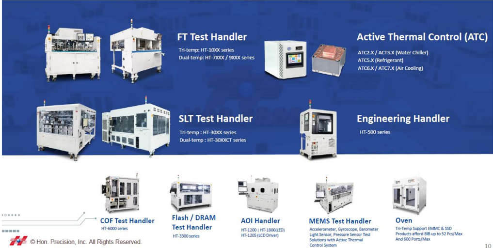
Source: Company data, Nomura research
Fig. 234: Hon's tool order mix by application
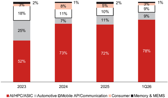
Source: Company data, Nomura research
3%
9%
9%
1%
Fig. 235: Hon - global footprint
China(Suzhou) Subsidiary
Hon. Precision
(Taiwan Headquarter)
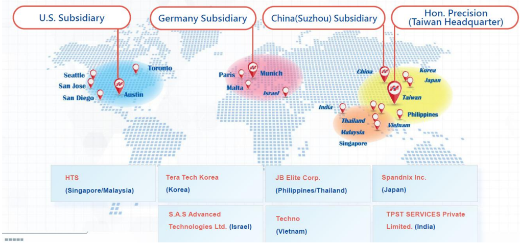
Source: Company data, Nomura research
Fig. 236: Hon - company milestones
| Year | Event |
|---|---|
| 1999 | Wen-Ta Hsieh, Jung-Li Chang Chien, and Te-Kuei Weng founded Hon. Technology, dedicated to handler production. |
| 2015 | Hon. Precision was established to replace Hon. Technology. |
| 2016 | Established a China subsidiary, Hon. Precision Technology (Suzhou). |
| 2020 | The Suzhou subsidary began leasing the Shengpu Plant. |
| 2022 | Established a US subsidiary, Hon. Precision, USA Inc. The Longshan Plant of Hon. Precision in Taiwan was operational. |
| 2023 | New plant completion. |
| 2024 | The Suzhou subsidary's own Changshu Plant was operational. Listed on TPEX Emerging Board in October. |
| 2025 | Established a Germany subsidiary, Hon. Precision, Germany GmbH. Listed on TWSE in November. |
| 2026 | Acquired a new piece of land in Taichung, Taiwan. |
Source: Company data, Nomura research
Fig. 237: Hon - factory sites and planning
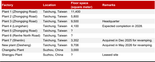
| Factory | Location | Floor space (square meter) | Remarks |
|---|---|---|---|
| Plant 1 (Zhongqing Road) | Taichung, Taiwan | 11,400 | |
| Plant 2 (Zhongqing Road) | Taichung, Taiwan | 5,800 | |
| Plant 3 (Zhongqing Road) | Taichung, Taiwan | 9,500 | Headquarter |
| Plant 4 (Longshan) | Taichung, Taiwan | 4,100 | Expected completion in 2028. |
| Plant 5 (Zhongqing Road) | Taichung, Taiwan | ? | |
| Plant 6 (Renhe North Road) | Taichung, Taiwan | ? | |
| Plant 7 (Shenlin) | Taichung, Taiwan | 3,352 | Acquired in Dec 2025 for revamping. |
| New plant (Desheng) | Taichung, Taiwan | 9,706 | Acquired in May 2026 for revamping. |
| Changshu Plant | Suzhou, China | 3,000 | |
| Shengpu Plant | Suzhou, China | ? | Leased site |
Source: Company data, Nomura research
Fig. 238: Board of directors
Other senior vehicles, 2.4%
9,000
7,500
6,000
20%
15%
| Title | Name | Individual ownership | Background | Remarks |
|---|---|---|---|---|
| Chairman | Wen-Ta Hsieh | 1.8% | Department of Mechanical Design, National Taipei Institute of Technology Chairman of Hon. Precision | Co-founder. Representative of Hung Min Development Co., Ltd. (17.4% ownership). |
| Director | Jung-Li Chang Chien | 0.7% | Department of Electronic Engineering, Feng Chia University President of Hon. Precision | Co-founder. Representative of Hongji Investment Co., Ltd. (12.1% ownership). |
| Director | Te-Kuei Weng | 0.2% | Department of Electrical Engineering, Chung Hua University Director of King Yuan Electronics Vice President of Hon. Precision | Co-founder. Representative of Hong Cheng Investment Co., Ltd. (4.7% ownership). |
| Director | Chen-Ming Chao | 0.3% | Department of Information Engineering, Feng Chia University Assistant Vice President of the Sales Department at Hon. Precision | A relative of the Chairman. Representative of Laiyu Investment Co., Ltd. (2.5% ownership). |
| Director | Yu-Cheng Li | 0.0% | Ph.D of Industrial Engineering, National Tsing Hua University Vice President of Ever Supreme Bio Technology | |
| Director | Tzu-Sheng Wu | 0.0% | Master of Laws, National Taiwan University Master of Laws, Duke University Director-General, Legal Affairs Bureau of Taichung City Government Chairperson, Taichung Bar Association | |
| Independent director | Hui-Chu Weng | 0.0% | Ph.D of Mechanical Engineering, National Cheng Kung University Associate Professor of the Department of Mechanical Engineering, Chung Yuan Christian University | |
| Independent director | Yao-Kuei Hsiao | 0.0% | Ph.D of Material Science and Engineering, National Taiwan University of Science and Technology Committee Member of the Investment Review Committee Convener, National Development Fund, Executive Yuan | |
| Independent director | Chia-Hui Cheng | 0.0% | Manager, Deloitte & Touche Accountant, Haps Consulting Ltd. & CPAs Accountant, Chungsun Prime CPA |
Note: Data as of May 2026.
Source: Company data, Nomura research
Fig. 239: Hon's shareholder structure
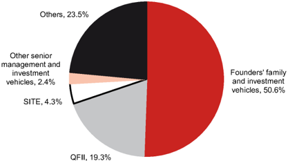
Note: Data as of 22 July 2026.
Source: Company data, Nomura research
Fig. 240: Share price vs SITE and QFII ownership
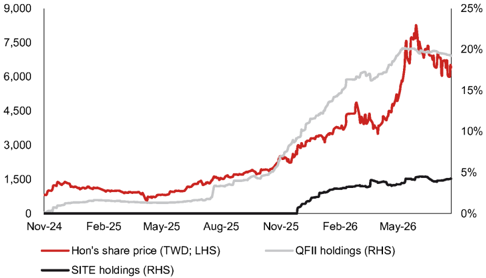
Note: Data of 22 July 2026.
Source: TEJ, Nomura research
Relative performance chart
EQUITY: TECHNOLOGY
Price
(TWD)
2500 -
20001
15001
10001
5001
300
-250.
- 200
-150
Chroma ATE Inc. 2360.TW 2360 TT
EQUITY: TECHNOLOGY
Churra. I CEC Namura
Full power on the bright AI avenue
Riding on upgrades in AI/HPC chips and server power, with CPO test joining the lineup; resume at Buy
Resume coverage at Buy with TP of TWD2,845, implying ~34% upside
We resume coverage of Chroma with a Buy rating and a target price of TWD2,845, based on 38x average 2027-28F EPS of TWD74.9. Our target P/E multiple is at the higher end of Chroma's historical trading band of 14-58x, which we view as reasonable given a 39% net earnings CAGR through 2026-28F. The stock trades at 32x 2027F basic EPS of TWD65.6, compared to semi backend equipment/test interface vendors (Bloomberg consensus 2027E average P/E: 37x) and data center power peers (average: 27x). Chroma is a testing equipment maker primarily serving semi/photonics (38% of 2026F consolidated revenue) and power electronics (38%) customers. In semi/photonics, we expect Chroma to ride on the secular testing tailwinds from increasing design complexity and larger footprints particularly in AI/HPC chips, as well as the emergence of copackaged optics (CPO) test insertions as a longer-term driver. In test instrument & automatic testing system (ATS), we believe Chroma is well-positioned to monetize the transition of the AI server power architecture toward high-voltage direct current (HVDC; ±400V or 800V) power racks. We expect Chroma to record a revenue CAGR of 32% and model basic EPS of TWD43.6/TWD65.6/TWD84.2 in 2026F/27F/28F. Major downside risks to our view are CoWoS
and backend testing capacity expansion slowdown and delayed HVDC deployments.
Handler upgrades and broader SLT adoption underway
We believe Chroma's system-level test (SLT) handler will enjoy a regular upgrade cycle given AI/HPC platform refresh cadences, and will particularly capitalize on the ASP uptrend from nVidia's (NVDA US, Not rated) adoption of GPU-on-GPU SoIC in 2028E for more stringent thermal control. In our view, TSMC (2330 TT, Buy) and OSATs' more aggressive 2.5D/CoWoS capacity investments and more spending on testing by AI OSATs could be positive indicators for Chroma's SLT business, and we see potentially more SLT adoption by AI/HPC chips in the longer run. We expect a 68% revenue CAGR for Semi/Photonics over 2025-28F.
Intact HVDC adoption, and Chroma benefits from more complicated testing
Despite recent market concerns about slower-than-expected HVDC adoption, we believe the adoption trajectory remains intact. A top US CSP is en-route to adopting ±400VDC from 2H26F, likely beginning with VR200 racks before extending the architecture to its own ASIC racks. More sophisticated testing efforts, in our view, remain a key positive for Chroma, and we model an ATS revenue CAGR of 43% over 2025-28F.
| Year-end 31 Dec Currency (TWD) | FY25 Actual | Old | FY26F New | Old | FY27F New | Old | FY28F New |
|---|---|---|---|---|---|---|---|
| Revenue (mn) | 28,311 | 0 | 53,514 | 0 | 74,977 | 0 | 93,623 |
| Reported net profit (mn) | 11,692 | 0 | 18,471 | 0 | 27,778 | 0 | 35,687 |
| Normalised net profit (mn) | 11,692 | 0 | 18,471 | 0 | 27,778 | 0 | 35,687 |
| FD normalised EPS | 27.59 | 43.42 | 65.30 | 83.90 | |||
| FD norm. EPS growth (%) | 121.7 | 57.4 | 50.4 | 28.5 | |||
| FD normalised P/E (x) | 77.0 | - | 48.9 | - | 32.5 | - | 25.3 |
| EV/EBITDA (x) | 83.7 | - | 37.3 | - | 25.0 | - | 19.2 |
| Price/book (x) | 28.2 | - | 21.3 | - | 15.7 | - | 12.3 |
| Dividend yield (%) | 0.9 | - | 1.4 | - | 2.2 | - | 2.8 |
| ROE (%) | 41.2 | 49.8 | 55.8 | 54.6 | |||
| Net debt/equity (%) | net cash | net cash | net cash | net cash |
Source: Company data, Nomura estimates
Global Markets Research 24 July 2026
| Rating From Suspended | Buy |
|---|---|
| Target price From N/A | TWD 2,845.00 |
| Closing price 22 July 2026 | TWD 2,125.00 |
| Implied upside | +33.9% |
| Market Cap (USD mn) | 27,951.6 |
| ADT (USD mn) | 217.9 |
Relative performance chart
Source: LSEG, Nomura
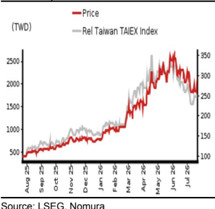
Research Analysts
Taiwan Technology
Eric Chen, CFA - NITB eric.chen@nomura.com +886(2) 21769965
Aaron Jeng, CFA - NITB
aaron.jeng@nomura.com +886(2) 21769962
Anne Lee, CFA - NITB
anne.lee@nomura.com +886(2) 21769966
Vivian Yang - NITB
vivian.yang@nomura.com +886(2) 21769970
Key data on Chroma ATE Inc.
Performance
| (%) | 1M | 3M | 12M | ||
|---|---|---|---|---|---|
| Absolute (TWD) | -8 | 4.7 | 400 | M cap (USDmn) | 27,951.6 |
| Absolute (USD) | -9.9 | 1.9 | 355.9 | Free float (%) | 81.9 |
| Rel to Taiwan TAIEX Index | -0.7 | -12.1 | 307.6 | 3-mth ADT (USDmn) | 217.9 |
Income statement (TWDmn)
| Year-end 31 Dec | FY24 | FY25 | FY26F | FY27F | FY28F |
|---|---|---|---|---|---|
| Revenue | 21,604 | 28,311 | 53,514 | 74,977 | 93,623 |
| Cost of goods sold | -8,858 | -10,886 | -20,098 | -27,806 | -34,006 |
| Gross profit | 12,746 | 17,425 | 33,416 | 47,171 | 59,617 |
| SG&A | -7,264 | -8,227 | -10,957 | -13,491 | -16,232 |
| Employee share expense | 0 | 0 | 0 | 0 | 0 |
| Operating profit | 5,482 | 9,198 | 22,458 | 33,680 | 43,385 |
| EBITDA | 6,257 | 10,038 | 23,429 | 35,077 | 45,390 |
| Depreciation | -775 | -841 | -971 | -1,398 | -2,005 |
| Amortisation | 0 | 0 | 0 | 0 | 0 |
| EBIT | 5,482 | 9,198 | 22,458 | 33,680 | 43,385 |
| Net interest expense | 48 | 56 | 48 | 65 | 96 |
| Associates & JCEs | 669 | 734 | 759 | 1,022 | 1,143 |
| Other income | 510 | 3,930 | 155 | 0 | 0 |
| Earnings before tax | 6,709 | 13,918 | 23,421 | 34,767 | 44,623 |
| Income tax | -1,308 | -1,992 | -4,686 | -6,749 | -8,696 |
| Net profit after tax | 5,400 | 11,926 | 18,735 | 28,018 | 35,927 |
| Minority interests | -136 | -234 | -264 | -240 | -240 |
| Other items | 0 | 0 | 0 | 0 | 0 |
| Preferred dividends | 0 | 0 | 0 | 0 | 0 |
| Normalised NPAT | 5,264 | 11,692 | 18,471 | 27,778 | 35,687 |
| Extraordinary items | 0 | 0 | 0 | 0 | 0 |
| Reported NPAT | 5,264 | 11,692 | 18,471 | 27,778 | 35,687 |
| Dividends | -3,828 | -8,292 | -12,930 | -19,445 | -24,981 |
| Transfer to reserves | 1,436 | 3,400 | 5,541 | 8,333 | 10,706 |
| Valuations and ratios | |||||
| Reported P/E (x) | 170.1 | 76.7 | 48.7 | 32.4 | 25.2 |
| Normalised P/E (x) | 170.1 | 76.7 | 48.7 | 32.4 | 25.2 |
| FD normalised P/E (x) | 170.8 | 77.0 | 48.9 | 32.5 | 25.3 |
| Dividend yield (%) | 0.4 | 0.9 | 1.4 | 2.2 | 2.8 |
| Price/cashflow (x) | 187.9 | 171.3 | 69.7 | 47.1 | 26.7 |
| Price/book (x) | 36.2 | 28.2 | 21.3 | 15.7 | 12.3 |
| EV/EBITDA (x) | 130.5 | 83.7 | 37.3 | 25.0 | 19.2 |
| EV/EBIT (x) | 146.9 | 90.8 | 38.9 | 26.0 | 20.1 |
| Gross margin (%) | 59.0 | 61.5 | 62.4 | 62.9 | 63.7 |
| EBITDA margin (%) | 29.0 | 35.5 | 43.8 | 46.8 | 48.5 |
| EBIT margin (%) | 25.4 | 32.5 | 42.0 | 44.9 | 46.3 |
| Net margin (%) | 24.4 | 41.3 | 34.5 | 37.0 | 38.1 |
| Effective tax rate (%) | 19.5 | 14.3 | 20.0 | 19.4 | 19.5 |
| Dividend payout (%) | 72.7 | 70.9 | 70.0 | 70.0 | 70.0 |
| ROE (%) | 22.5 | 41.2 | 49.8 | 55.8 | 54.6 |
| ROA (pretax %) | 19.7 | 26.8 | 47.7 | 52.7 | 55.4 |
| Growth (%) | |||||
| Revenue | 15.7 | 31.0 | 89.0 | 40.1 | 24.9 |
| EBITDA | 15.5 | 60.4 | 133.4 | 49.7 | 29.4 |
| Normalised EPS | 32.3 | 121.7 | 57.4 | 50.4 | 28.5 |
| Normalised FDEPS | 32.3 | 121.7 | 57.4 | 50.4 | 28.5 |
Source: Company data, Nomura estimates
Cashflow statement (TWDmn)
| Year-end 31 Dec | FY24 | FY25 | FY26F | FY27F | FY28F |
|---|---|---|---|---|---|
| EBITDA | 6,257 | 10,038 | 23,429 | 35,077 | 45,390 |
| Change in working capital Other operating cashflow | -5,568 4,094 | -3,098 | -5,964 | -9,183 -6,684 | -2,906 |
| Cashflow from operations | 4,784 | -1,682 | -4,496 | 19,211 | -8,600 33,883 |
| expenditure | 5,258 | 12,970 | -5,998 | -7,490 | |
| Capital | -2,005 | -2,301 | -3,727 | ||
| Free cashflow | 2,779 | 2,957 | 9,243 | 13,213 | 26,393 |
| Reduction in investments | -340 | -251 | -1,701 | 0 | 0 |
| Net acquisitions | 0 | 0 | 0 | 0 | 0 |
| Dec in other LT assets | 0 | 0 | 0 | 0 | 0 0 |
| Inc in other LT liabilities Adjustments | 0 454 | 0 | 0 | 0 0 | |
| 3,980 | 255 | 0 | |||
| CF after investing acts | 2,893 | 6,686 | 7,797 | 13,213 | 26,393 |
| Cash dividends | -2,897 | -3,905 | -8,292 | -12,930 | -19,445 |
| Equity issue | 0 | 0 | 0 | 0 | 0 |
| Debt issue | 393 | -200 | 35 | 0 | 0 |
| Convertible debt issue | 0 | 0 | 0 | 0 | 0 |
| Others | -422 | -459 | -35 | 0 | 0 |
| CF from financial acts | -2,926 | -4,563 | -8,292 | -12,930 | -19,445 |
| Net cashflow | -33 | 2,123 | -496 | 283 | 6,949 |
| Beginning cash | 4,132 | 4,099 | 6,222 | 5,727 | 6,009 |
| Ending cash | 4,099 | 6,222 | 5,727 | 6,009 | 12,958 |
| Ending net debt | -574 | -2,904 | -2,372 | -2,655 | -9,603 |
| Balance sheet (TWDmn) | |||||
| As at 31 Dec | FY24 | FY25 | FY26F | FY27F | FY28F |
| Cash & equivalents | 4,099 | 6,222 | 5,727 | 6,009 | 12,958 |
| Marketable securities | 941 | 2,092 | 3,747 | 3,747 | 3,747 |
| Accounts receivable | 6,070 | 8,925 | 16,073 | 23,957 | 26,604 |
| Inventories | 5,458 | 7,919 | 10,704 | 15,732 | 17,003 |
| Other current assets | 856 | 967 | 1,351 | 1,351 | 1,351 |
| Total current assets | 17,425 | 26,126 | 37,601 | 50,797 | 61,662 |
| LT investments | 8,918 | 7,953 | 8,791 | 9,814 | 10,956 |
| Fixed assets | 6,956 | 7,232 | 10,059 | 14,659 | 20,144 |
| Goodwill | 0 | 0 | 0 | 0 | 0 |
| Other intangible assets | 0 | ||||
| Other LT assets | 0 4,009 | 0 5,839 | 0 5,797 | 0 5,797 | 5,797 |
| Total assets | 37,308 | 47,150 | 62,249 | 81,067 | 98,560 |
| Short-term debt | 1,417 | 14 | 305 | 305 | 305 |
| Accounts payable | 3,106 | 4,116 | 6,190 | 9,097 | 9,832 |
| Other current liabilities | 3,711 | 5,030 | 7,308 | 8,130 | 8,406 |
| Total current liabilities | 8,235 | 9,159 | 13,802 | 17,532 | 18,543 |
| Long-term debt | 2,108 | 3,304 | 3,050 | 3,050 | 3,050 |
| Convertible debt | 0 | 0 | 0 | 0 | 0 |
| Other LT liabilities | 1,515 | 2,125 | 2,082 | 2,082 | 2,082 23,676 |
| Total liabilities | 11,858 | 14,587 | 18,935 | 22,665 | |
| Minority interest | 573 | 665 | 972 | 1,212 | 1,452 |
| Preferred stock | 0 | 0 | 0 | 0 | 0 |
| Common stock | 8,851 | 8,465 | 8,518 | 8,518 | 8,518 |
| Retained earnings | 15,163 | 22,825 | 32,990 | 47,838 | 64,081 |
| Proposed dividends | 0 | 0 | 0 | 0 | 0 833 |
| Other equity and reserves | 863 | 608 | 833 | 833 | |
| Total shareholders' equity | 24,877 | 31,898 | 42,341 | 57,189 | 73,432 |
| Total equity & liabilities | 37,308 | 47,150 | 62,249 | 81,067 | 98,560 |
| Liquidity (x) | |||||
| Current ratio | 2.12 | 2.85 | 2.72 | 2.90 | 3.33 |
| Interest cover | - | - | - | - | - |
| Leverage Net debt/EBITDA (x) | net cash | net cash | net cash | net cash | net cash |
| Net debt/equity (%) | net cash | net cash | net cash | net cash | net cash |
| Per share | |||||
| Reported EPS (TWD) | 12.49 | 27.70 | 43.59 | 65.56 | 84.23 |
| Norm EPS (TWD) | 12.49 | 27.70 | 43.59 | 65.56 | 84.23 |
| FD norm EPS (TWD) | 12.44 | 27.59 | 43.42 | 65.30 | 83.90 |
| BVPS (TWD) | 58.72 | 75.30 | 99.96 | 135.01 | 173.36 |
| DPS (TWD) | 9.04 | 19.58 | 30.52 | 45.90 | 58.97 |
| Activity (days) | |||||
| Days receivable | 102.6 | 96.7 | 85.3 | 97.4 | 98.8 |
| Days inventory | 224.9 | 224.3 | 169.1 | 173.5 | 176.2 |
| Days payable | 128.0 | 121.1 | 93.6 | 100.3 | 101.9 |
| Cash cycle | 199.5 | 199.9 | 160.8 | 170.6 | 173.1 |
Source: Company data, Nomura estimates
Company profile
Chroma is a world leading supplier of precision test and measurement instrumentation, automated test systems, intelligent manufacturing systems, and test & automation turnkey solutions.
Valuation Methodology
Our TP of TWD2,845 is based on 38x average 2027-28F EPS, at the higher end of Chroma's historical trading band (14-58x). The benchmark of this stock is TAIEX.
Risks that may impede the achievement of the target price
Major downside risks to our call include: 1) CoWoS and backend testing capacity expansion slowdown; 2) slower-than-expected product refresh, platform performance upgrade, or ramp-up by the AI chip end customers; 3) fiercer-than-expected from other international testing equipment makers; and 4) weaker-than-expected end-market demand, particularly for AI servers.
ESG
The company is fully aware of climate change and the need for carbon reduction. It is dedicated to minimize the use of energy and resources as well as reducing the amount of waste produced in manufacturing processes. At the same time, Chroma has been continuously committed to social welfare and care for underprivileged groups and young children.
Industry Supply Chain
Semiconductor/Photonic Test - AI/HPC and CPO pave growth trajectory IC
We estimate Chroma's Semiconductor/Photonic Test business to register a 68% revenue CAGR over 2025-28F, riding on the secular semiconductor testing tailwinds from increasing design complexity and larger footprints particularly in AI/HPC chips, as well as the emergence of CPO. Chroma derives 38% of its revenue from Semiconductor/Photonic Test in 2026F, in which we estimate a 70-80% and 20-30% split between semiconductor and photonics, with the company mainly providing test handlers for SLT used in niche, quality-dependent verticals like AI/HPC.
We believe Chroma's SLT handlers will enjoy an intense equipment upgrade cycle given regular AI/HPC platform refresh cadences, and will particularly capitalize on the ASP uptrend from nVidia's AI GPU migration to SoIC stacking in 2028E for more stringent thermal control requirements (we estimate nVidia currently accounts for ~20% of Chroma' s total revenue). TSMC and OSATs' more aggressive 2.5D/CoWoS capacity investments and more testing spending by AI OSATs could be positive indicators for Chroma's SLT handler business, and we see potentially more SLT adoption by AI/HPC chips in the longer run as well, contemplating more unbearable field return costs. Thus far, Chroma has secured new SLT opportunities from Google (GOOGL US, Not rated) Axion CPU and AMD (AMD US, Not rated) MI450 series . We also like Chroma's progress into 2D/3D wafer metrology to capture another adjacency of advanced packaging capacity growth. Despite no uniform testing standard for CPO and uncertainty about ramp-up timeline, we expect Chroma's established experience in photonics to pave the way for its handler role in test insertion 3 and optical tester in test insertion 4 .
FT and SLT are Chroma's testing equipment addressable markets
The semiconductor backend processes are punctuated by a few test insertions that sort out defective silicon as early as possible to gate output quality chip probe (CP), final test (FT), burn-in test (BIT), and system-level test (SLT) , and the entire backend flows start with CP at the wafer level before the individual dies are cut out of the wafer and undergo subsequent assembly. We explore the IC backend testing process in our Anchor Report, and here we only focus on FT and SLT, which are Chroma's addressable segments.
Fig. 241: An illustration of semiconductor manufacturing and backend testing flows
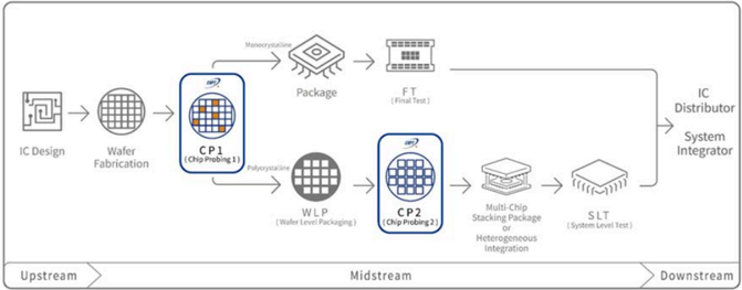
Source: CHPT, Nomura research
FT is a mandatory procedure , and depending on IC customers' configurations, there could be two or more FT steps during the manufacturing cycle (e.g., nVidia's AI GPUs require two FT steps, one before BIT and the other after BIT). FT is carried out after IC assembly (on substrates, lead frames, or wire bond) and chip packages are capable of accommodating larger input voltages or electric current than bare dies. FT measures electrical properties of chips given pre-programmed inputs to identify product functionality ('pass or fail' is the terminology) and sort functional products by grade (also known as
'binning'), all within the shortest possible time frame (usually hundreds or thousands of seconds) , as chip vendors may want to control test charges (measured by
'hourly rates') which are amortized expenses of costly testers.
We discuss digital IC testing in detail in this report. We note below three primary parameters that form a sequential filtering system in FT for logic circuits whose focuses are on whether outputs are 'correct'. By contrast, analog/mixed-signal IC testing places more emphasis on the 'measurement accuracy' of select parameters (e.g., linearity and signal-to-noise ratio).
- Direct current (DC) test: The DC test is the first phase in FT and consumes the least time amongst the three phases. It measures the steady-state electrical characteristics of the chip using direct current and ensures the physical silicon structure is intact. The DC test does not validate logic or speed, however. The primary metrics measured during this phase include: 1) open/short test - which verifies all pins are properly connected to the internal circuitry (no 'open') and that no pins are accidentally welded together (no 'short'); 2) leakage current - which ensures a pin does not 'bleed' excessive current into the substrate when it is given a specific voltage level; 3) power consumption - which detects the electric current drain inefficiency; and 4) output voltage level - which confirms the chip can drive signals out at the correct voltage thresholds required to communicate with other components. 1.
- Function test: The subsequent function test is to check whether the logic operation works properly. During the function test, the tester floods the chip with preprogrammed binary inputs (i.e., test vectors) and records the outputs generated by the chip to compare the results against the expected mathematical truth table. Function tests are typically executed at a nominal, conservative clock speed to isolate pure logical errors from high-speed timing anomalies. 2.
- Alternating current (AC) test: The AC test introduces the critical dimension of 'time', evaluating how the chip performs under dynamic, high-frequency AC conditions and checking the output signals' 'waveform', because a chip might have perfect structure and flawless logic responses at slow speeds. The AC test pushes the silicon to its physical limits by measuring sub-nanosecond timing parameters to ensure signals propagate cleanly across the die without corruption. Major test items include propagation delay, setup and hold times, rise and fall times, and maximum frequency. The AC test is also the foundation of 'binning' , sorting out the best-performing chips and lower-tiered ones. 3.
On the other hand, SLT is an optional procedure , during which the chip is inserted into a system test board designated by the chip vendor to simulate how it works in the realworld scenario. The test board is a modified version of the actual commercial motherboard that eventually houses the silicon and is equipped with other components such as memory and peripherals. The SLT boots a full operating system like Linux or Android and runs heavy, asynchronous software workloads to replicate genuine user environments. Throughout the process, SLT measures functional and behavioral metrics rather than raw structural data, including system stability, workload execution throughput, thermal throttling thresholds, and high-speed interface bit error rates (BER).
SLT has gained traction industry-wide because it exposes defect classes that the preceding stages structurally cannot. DC test, Function test, and AC test are largely deterministic and exercise the device in isolation, at fixed patterns and controlled conditions. They are effective at catching hard, static failures but are poorly suited to intermittent, workload-dependent or interaction-level defects - issues that only manifest when multiple IP blocks operate concurrently under realistic power, thermal, and timing stress, or under specific software-induced corner cases. As chip complexity has grown with heterogeneous integration, multi-core coherency, and higher-speed interfaces, these system-level 'test escapes' could result in a larger share of field returns, which has steered SLT from a niche practice in automotive/mobile applications toward broader adoption across compute, AI accelerator, and networking chips, where the cost of a return merchandise authorization (RMA) far outweighs the cost of additional test screening.
SLT Tester Site
FAB
ATE
Wafer Test
Assemble
System Level
Test
SLTI
Fig. 242: SLT acknowledges that software is part of the system, and recreates the enduse environment as closely as possible
(JTAG, SWD)
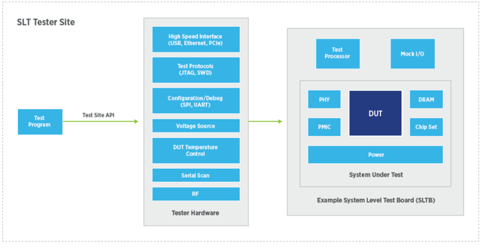
Good Devices
Test
Program
Bad Devices
Source: Teradyne, Nomura research
Fig. 243: Traditional test coverage becomes more challenging, and SLT's strategic importance is emerging
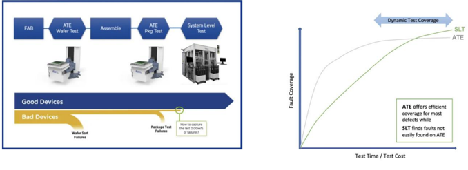
Source: Teradyne, Nomura research
The SLT phase is less expensive than FT given there is no usage of multi-million-dollar testers, but it is very time-consuming and could take minutes or even hours to execute per devices. At high volumes, the throughput mismatch could become the binding constraint on SLT adoption, since running every unit through hours of system-level workloads is economically impractical for most product lines. As such, the industry leans toward parallel testing inside automated SLT handlers, and potentially the integration of adaptive testing backed by machine learning algorithm which selectively routes only silicons at risk to extended SLT screening while the bulk of the chips proceed through a shortened or standard flow. This 'smart SLT' approach preserves most of the defectscreening benefit while containing the test time and cost overhead, and is emerging as a key differentiator among OSATs and IDMs competing on both quality (defined by defective parts per million, or DPPM) and test cost per unit.
Fault Coverage
ATE
Dynamic Test Coverage
Testing
Healthy
Fig. 244: Adaptive SLT could further reduce the overall cost (time) of test
(ATE)
System Level
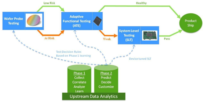
Source: AEM, Nomura research
IC test trios: ATE, prober/handler, and test interface
The semiconductor testing is not carried out by one single tool but a tightly integrated system also known as 'test cell'. The test cell consists of three major parts: automated test equipment (ATE), prober/handler, and application-specific test interfaces. In SLT, the ATE is replaced with a system test board on which test sockets are equipped, housed inside an SLT handler.
- Automated test equipment (ATE): ATE, or simply 'tester', is the sophisticated core workstation of the test cell that feeds precise electrical stimulus signals (e.g., voltages, currents, or high-frequency waveforms) into the device under test (DUT) and monitors the output responses. The tester compares the chip's real-time performance running on pre-programmed inputs against engineering design specifications to identify defectives. In the ATE architecture, the mainframe houses the tester's power supply, central cooling unit and the system controllers, and the test head houses the test interfaces. ·
- Prober/handler: The prober or the handler is the mechanical automation arm of the test cell that operates with the ATE to ensure a continuous, high-speed, and unmanned silicon test flows. The test head is flipped and pneumatically or hydraulically docked into the core mechanical nest of the prober/handler. The prober and the handler are used in different testing scenario the prober is present in CP and handles uncut wafers, using microscopic pins to physically contact with individual die before they are singulated, while the handler picks up chip packages (in FT or SLT) from trays, inserts them into the test sockets, and physically sorts them into different bins based on the tester's verdict. ·
- Test interface: The test interface is the physical and electrical 'bridge', customized based on the silicon layout/package, to connect the generic tester to the DUT. A probe card paired with pogo pins (or MEMS pins for fine-pitch applications) is being used in CP, while a load board with test sockets is adopted in FT. ·
Test head
Opening/closing
Fig. 245: A test cell in chip probe
Performance board -
Spring contact pin
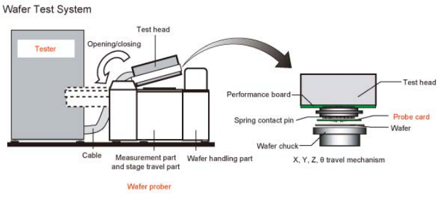
Source: MJC, Nomura research
Source: MJC, Nomura research
The IC test squad is not complete without 'role players'
Beside the aforementioned trios, we note there are also tools supplementing temperature management to prevent undesired shifts in chip performance and physical properties under different thermal conditions, and specialized plug-in modules to expand or reconfigure the tester's scope.
- Thermal chuck: During CP, the chuck is the flat, rigid metallic platform that holds the silicon wafer in place using vacuum suction. A thermal chuck is a chuck with built-in heating elements and internal cooling channels to uniformly control the temperature of the wafer under test when mimicking different thermal conditions in operations. A thermal chuck must demonstrate extreme planarity (i.e., very meager warpage) at extreme temperature swings to avoid poor electrical contacts or wafer crack by probe needles. ·
- Active thermal control system (ATC): ATC is a dynamic temperature management system integrated into the handler. When a tester boots up workloads, the DUT could undergo a spike in internal power density and instantaneously heat up. ATC detects the thermal conditions of the chip under test and instantly adjusts its cooling/heating action to counteract the chip's internal power fluctuations. ·
-
Instruments: The tester is essentially a modular chassis populated by a cluster of instruments that define its initial testing scope. However, if a silicon requires test coverage beyond this built-in set, specialized instruments can be added to the tester to extend its capabilities. These modular instruments are notably critical for highperformance domains like analog/mixed-signal and high-speed digital, and we observe optical instruments are introduced in CPO test insertions to assist with photonic test items (e.g., optical insertion loss, spectrum/wavelength and polarization effects). ·
-
Test head
Mainframe
Cable Bundle
(not seen)
Fig. 246: A test cell in final test
Test Head
Test Interface
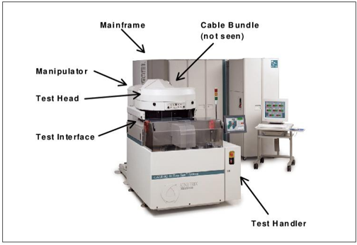
Source: SAE Technical Papers "Thermal Management and Control in Testing Packaged Integrated Circuit (IC) Devices", Nomura research
prober (right; by FormFactor)
Fig. 247: The thermal chuck is integrated into the wafer prober
Thermal chuck (left; by ATT Systems) and wafer prober (right; by FormFactor)
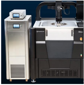
Source: FormFactor, Nomura research
Fig. 250: Semiconductor test equipment and interface maker overview
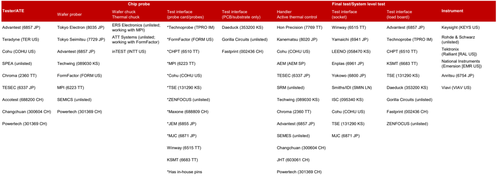
| Chip probe | Chip probe | Chip probe | Final test/System level test | Final test/System level test | Final test/System level test | Final test/System level test | Final test/System level test | |
|---|---|---|---|---|---|---|---|---|
| Tester/ATE | Wafer prober | Wafer chuck Thermal chuck | Test interface (probe card/probes) | Test interface (PCB/substrate only) | Handler Active thermal control | Test interface (socket) | Test interface (load board) | Instrument |
| Advantest (6857 JP) | Tokyo Electron (8035 JP) | ERS Electronics (unlisted; working with MPI) | *Technoprobe (TPRO IM) | Daeduck (353200 KS) | Hon Precision (7769 TT) | Winway (6515 TT) | Advantest (6857 JP) | Keysight (KEYS US) |
| Teradyne (TER US) | Tokyo Seimitsu (7729 JP) | ATT Systems (unlisted; working with FormFactor) | *FormFactor (FORM US) | Gorilla Circuits (unlisted) | Kanematsu (8020 JP) | Yamaichi (6941 JP) | Technoprobe (TPRO IM) | Rohde & Schwarz (unlisted) |
| Cohu (COHU US) | Advantest (6857 JP) | inTEST (INTT US) | *CHPT (6510 TT) | Fastprint (002436 CH) | Cohu (COHU US) | LEENO (058470 KS) | CHPT (6510 TT) | Tektronix (Ralliant [RAL US]) |
| SPEA (unlisted) | Techwing (089030 KS) | *MPI (6223 TT) | AEM (AEM SP) | Enplas (6961 JP) | KSMT (6683 TT) | National Instruments (Emersion [EMR US]) | ||
| Chroma (2360 TT) | FormFactor (FORM US) | *Cohu (COHU US) | TESEC (6337 JP) | Yokowo (6800 JP) | TSE (131290 KS) | Anritsu (6754 JP) | ||
| TESEC (6337 JP) | MPI (6223 TT) | *TSE (131290 KS) | SRM (unlisted) | Smiths/IDI (SMIN LN) | Daeduck (353200 KS) | Viavi (VIAV US) | ||
| Accotest (688200 CH) | SEMICS (unlisted) | *ZENFOCUS (unlisted) | Techwing (089030 KS) | ISC (095340 KS) | Gorilla Circuits (unlisted) | |||
| Changchuan (300604 CH) | Powertech (301369 CH) | *Maxone (688809 CH) | Chroma (2360 TT) | Cohu (COHU US) | Fastprint (002436 CH) | |||
| Powertech (301369 CH) | *JEM (6855 JP) | Advantest (6857 JP) | TSE (131290 KS) | ZENFOCUS (unlisted) | ||||
| *MJC (6871 JP) | SEMES (unlisted) | MJC (6871 JP) | ||||||
| Winway (6515 TT) | Changchuan (300604 CH) | |||||||
| KSMT (6683 TT) | JHT (603061 CH) | |||||||
| *Has in-house pins | Powertech (301369 CH) |
Source: Company data, Nomura research
Chroma is an expert in niche testers and ATC/handlers
Chroma has strategically positioned itself in the semiconductor backend testing arena with a focus on niche applications, rather than chasing the broad-market, leading-edge ATE segment dominated by the largest global players such as Advantest (6857 JP, Buy) and Teradyne (TER US, Not rated). Chroma's focus is most visible in ATC (named 'temperature forcing systems' at Chroma) and /handlers (primarily pick-and-place handlers, which uses suction to transfer the DUT and press it into the test sockets) and SoC testers for mature logic or analog/mixed-signal semi.
In ATC/handlers, the company specializes in FT/SLT ( with more focus on SLT ) and offers both dual-temp (high temperature [up to 150°C] and ambient temperature [around 25°C]) and tri-temp (high temperature, ambient temperature, and low temperature [down to -70°C]) ATC capabilities. Chroma's handlers add multi-site flexibility across single, dual, quad, octa-site configurations or more. AI/HPC applications , for instance, is a Chroma's target vertical for SLT handlers, and we believe nVidia is a key customer of Chroma.
On the SoC tester side, Chroma's niche is mature-node logic or analog/mixed-signal semi such as microcontroller units (MCUs) and power management ICs (PMICs), supporting global fabless and IDM customers, as well as Chinese ones, rather than competing head to head with global leading players in the advanced logic test.
Tester+ FT Handler+ATC System
WV KEYSIGHT
Fig. 248: The ATC is integrated into the handler
Tester
Source: Hon Precision, Nomura research
Fig. 249: The instrument helps expand dedicated test coverage
Source: Keysight, Nomura research
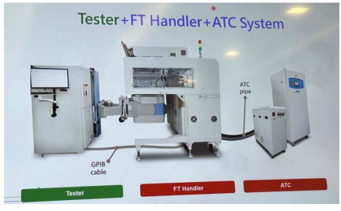
Source: Hon Precision, Nomura research
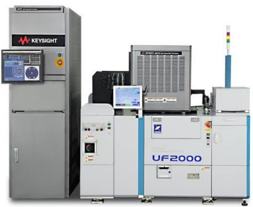
Source: Keysight, Nomura research
Fig. 251: Chroma's semiconductor test solutions
SOC/Analog Test Systems
SOC/Analog Test Systems
Front-end Process:
Wafer Fabrication
Lithography,
Etch, Implant
Wafer Clean
VLSI Test Systems
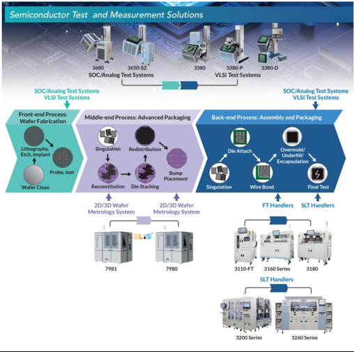
Source: Company data, Nomura research
Taiwan peer comparison - Chroma has little overlap with Hon. Precision
A frequently asked question by investors is whether and where Chroma competes with another Taiwan-based backend testing equipment maker Hon. Precision (7769 TT, Buy). Admittedly, both the companies have ATC/handler offerings for FT and SLT, but we believe they have fairly little business overlap given Chroma's focus on SLT handlers (we estimate 60-70% of Chroma's semiconductor testing revenue comes from SLT) vs Hon's focus on FT handlers (70-80% of handler revenue comes from FT).
Hon has been making inroads into the SLT handler market by leveraging its competency in customization and ATC, and we believe AMD is one of its longstanding customers in SLT handlers, although we think Chroma could have secured SLT handlers for AMD's latest MI400-series. We are aware that Hon has started engineering collaboration with nVidia in SLT handlers for the future generation of AI GPUs, but we are uncertain about whether Hon could really challenge Chroma's dominance in this segment. In our view, Hon's new SLT handler opportunities could lie squarely within ASIC customers whose broader adoptions of SLT, apart from mandatory FT, have significantly increased.
for mass parallelism
Temperature Forcing Systems
Fig. 252: Chroma's temperature forcing system can be seamlessly integrated into Chroma's handlers and optimized for mass parallelism
Eco Refrigerant Recirculated
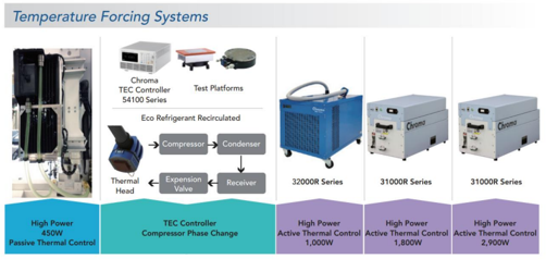
High Power
450W
Passive Thermal Control
Source: Company data, Nomura research
Source: Company data, Nomura research
Fig. 253: Comparison of major global tester and handler makers
| USD mn | Headquarter | Market cap | 2025 revenue | Revenue mix | Revenue mix | 2025 GM | 2025 OPM 2025 net profit | 2025 OPM 2025 net profit | 2025 OPM 2025 net profit | Handler |
|---|---|---|---|---|---|---|---|---|---|---|
| USD mn | Headquarter | Market cap | 2025 revenue | Tester | Handler | 2025 GM | Tester | Handler | ||
| Chroma ATE (2360 TT) | Taiwan | 24,332.8 | 908.4 | 10-15% | 20-25% | 61.5% | 32.5% | 375.2 | Mature logic/analog | FT 30-40%, SLT 60-70% Mostly logic/analog |
| Advantest (6857 JP) | Japan | 123,945.2 | 6,902.1 | 82% | <5% | 62.4% | 39.7% | 1,927.8 | 80% Logic/Analog 20% Memory | FT, SLT Mostly memory |
| Teradyne (TER US) | US | 50,462.1 | 3,190.0 | 75% | 15% | 58.3% | 22.3% | 632.1 | 80% Logic/Analog 20% Memory | SLT Mostly logic/analog |
| Cohu (COHU US) | US | 2,414.9 | 453.0 | ~40% | ~40% | 43.3% | 0.5% | (10.1) | Mature logic/analog | FT, SLT Mostly logic/analog |
| Hon. Precision (7769 TT) | Taiwan | 33,781.0 | 971.3 | n.a. | c.80% | 56.5% | 49.7% | 396.6 | n.a. | FT 70-80%, SLT 20-30% Mostly logic/analog |
| Kanematsu (8020 JP) | Japan | 2,157.8 | 7,062.3 | n.a. | <5% | 15.7% | 4.4% | 215.8 | n.a. | FT, SLT (from Seiko Epson) Mostly logic/analog |
| TESEC (6337 JP) | Japan | 75.5 | 37.6 | 45% | 36% | 37.8% | 5.7% | 2.0 | Mature logic/analog Discrete | FT (from Yokogawa) Mostly logic/analog |
| Techwing (089030 KS) | South Korea | 1,222.7 | 112.0 | n.a. | 36% | 42.2% | 10.0% | 6.6 | n.a. | FT Mostly memory |
| SEMES (unlisted) | South Korea | n.a. | n.a. | n.a. | n.a. | n.a. | n.a. | n.a. | FT Mostly memory | |
| AEM (AEM SP) | Singapore | 2,137.2 | 305.6 | 30% | 30% | 25.7% | 5.9% | 13.0 | Mature logic/analog | FT, SLT Mostly logic |
| Changchuan (300604 CH) | China | 26,090.7 | 736.2 | c.60% | c.30% | 55.1% | 24.4% | 185.2 | Logic/Analog Discrete | FT, SLT Logic/Analog, Discrete |
| Accotest (688200 CH) | China | 11,034.7 | 187.3 | c.90% | n.a. | 73.8% | 36.5% | 74.6 | Logic/Analog Discrete | n.a. |
| JHT (603061 CH) | China | 3,917.9 | 97.1 | n.a. | c.90% | 52.2% | 30.5% | 24.6 | n.a. | FT, SLT Logic/Analog, Discrete |
| Powertech (301369 CH) | China | 2,233.8 | 49.3 | c.85% | c.85% | 55.7% | -3.1% | 4.7 | Logic/Analog Discrete | FT Logic/Analog, Discrete |
Note: Market cap data as of July 17, 2026
Source: Company data, Bloomberg Finance LP, Nomura estimates
Increasing design complexity and larger footprints of AI/HPC chips spur structural testing growth
We believe increasing chip design complexity and larger package footprints are the two most critical catalysts inside AI/HPC chips that are fostering structural growth in the semiconductor testing process, an often overlooked element in the manufacturing value chain because of its relatively low portion in the cost structure. The semiconductor industry is currently undergoing a paradigm shift in layout/architecture by embracing a chiplet-based design philosophy, 2.5D advanced packaging to stitch multiple-reticle-sized interposers and 3D IC stacking to increase performance per area (measured by transistor density), as conventional geometric scaling slows, costs for chip design and yielding large die continue to rise at more advanced logic nodes (Fig. 254 , Fig. 255 , and Fig. 256 ), and any single chip inevitably faces the physical limit of reticle size (26x33mm exposure field size, or 858mm 2 ). In a seminar during SEMICON Taiwan 2025, TSMC estimated compute performance per reticle improvement by 80x from N28 to A16, and the incorporation of advanced packaging could enlarge the gain to ~320x at >9.5x-reticle CoWoS (Fig. 257 ).
advanced nodes
800
700
600
500
400
300
200
100
0
Normalized Cost/yield mm
5.0
4.5
N-7
Technology Scaling Propels Energy Efficient Compute
Fig. 254: The cost per yielded die vs node migration The cost per yielded die continue to increase when entering into more advanced nodes
3.0
2.5
2.0
1.5
28nm
1.0
0.5
0.0
Fig. 255: Cost reduction by using chiplets vs SoC solution
3 chips chiplet cost: 0.77x
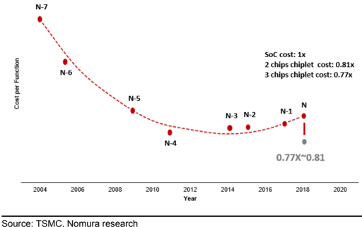
Cost per Function
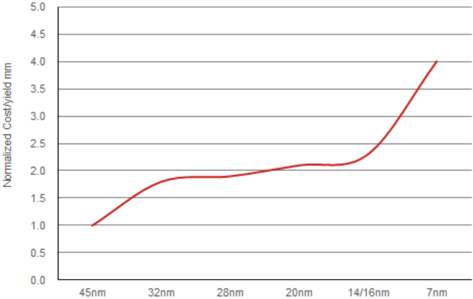
Source: Nomura research
Fig. 256: Skyrocketing chip design cost moving to more advanced nodes
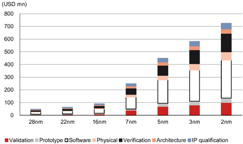
Source: IBS, Nomura research
While these innovations enable unprecedented computing power for AI/HPC, they have fundamentally altered the economics and mechanics of semiconductor manufacturing. Die-to-die interconnect in chiplets or 2.5D/3D packaging is a complex jigsaw puzzle replacing traditional seamless on-die communication, because engineers must ensure robust signal and power integrity , and thermal management and mechanical stress control also become crucial in such layouts. Consequently, we believe semiconductor testing is no longer just a routine quality-control process at the end of the production flows, and has become an indispensable, high-stakes discipline that directly dictates commercial success.
As device complexity increases, a longer testing time is needed, and if we take nVidia AI GPUs as examples and index the SLT time of Hopper to 1, we reach 1.5x for Blackwell's SLT time and 2.5x for Rubin's. In our view, the prolonged testing time and higher hourly rate should add to the testing content under cost. We estimate the overall testing content (defined as the sum of FT, BIT and SLT) in nVidia Rubin could rise to 3.3% of total cost vs. 2.5% for Blackwell and 1.9% for Hopper, based on our supply chain checks and analysis (Fig. 258 ). The lengthened testing time presents an outright tailwind for semiconductor testing equipment makers, in our view, given the need by OSATs to keep up with throughputs.
Compute Performance
(Ref: N28) (Speed x Density)
2004
Source: TSMC, Nomura research
Source: TSMC, Nomura research
Fig. 257: Advanced packaging is an approach to bring the subsystem performance further up
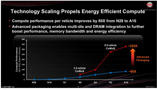
Source: TSMC, Nomura research
400
80%
60%
40%
20%
0%
Fig. 258: Increasing testing content in the logic manufacturing cost of nVidia AI GPUs
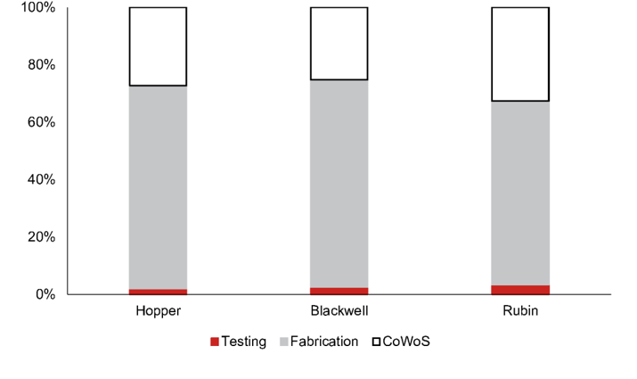
Source: Company data, Nomura estimates
More intense upgrade cycles for SLT handlers than FT handlers
We believe SLT handler upgrades are primarily driven by the tight coupling between the handler's mechanical and thermal interface and the physical design of each new AI chip platform. Unlike FT, which tests a packaged die in a relatively standardized form factor, SLT validates the chip at the full system or module level , indicating socket pin count, board layout, power delivery, and thermal load are all specific to that generation's module configurations.
Socket pin count is a key driver as each new AI/HPC chip tends to add more pins to support more power rails and higher I/O bandwidth. A pin-count change would therefore alter pin pitch, contact force distribution, and co-planarity tolerances, and the SLT socket typically must undergo redesign and re-qualification efforts when the AI chip moves to a new generation. The system test board layout compounds the changes, since system test boards are built to mirror the actual system operations including the power delivery network and high-speed signal topology, and the change in the system architecture could be very significant (e.g., from OAM+UBB in Hopper to Bianca in Blackwell).
Meanwhile, as AI/HPC silicon scale power density along with platform refresh cadence (even at an accelerated pace), the thermal subsystem has to scale in lockstep. Reliability and thermal control requirements during a test could also foster the upgrade vector. All in all, generation-specific parameters of AI/HPC chips necessitate test interface re-engineering, as well as compress the effective upgrade cycle and foster OSATs' purchases of new SLT handler platform at a higher ASP.
Compared to FT handlers, the generation-specific variables lead to a more frequent upgrade of SLT handlers. FT handlers could be insulated from full replacement as the core pick-and-place mechanics like trays, robotic arms and contact heads may persist across multiple device generations with the ATC and the mechanical conversion interface requiring regular updates. Although OSATs are adding ATC/handler capacity to address surging AI demand, we believe most of the upgrades (and therefore ASP growth) are within the ATC and with nearly no change in the handler - unless there is mechanical backbone redesign for larger trays or completely new device form factors (e.g., microchannel lids [MCL]).
More stringent thermal control requirements for SLT, moving toward SoIC
We believe Chroma will particularly capitalize on the ASP uptrend from nVidia's AI GPU migration to SoIC stacking, since the sub-system performance gain from more dies in a package comes at the cost of more stringent thermal requirements.
The max TDP of nVidia Blackwell Ultra (B300) is 1,400W, and we think the TDP of Rubin (R100) may start from 1,800W. We foresee further elevating thermal challenges moving to Feynman (F100), slated for 2028E (Fig. 23). nVidia at its GTC 2026 unveiled a plan to
Asomr
Dummy
2.5D vs. 3.5D Packaging
HBM4
HBM4
HBM4
HBM4
HBM4
adopt 3D stacking starting from the Feynman platform (report ). Vertical chip stacking (SoIC platform at TSMC) theoretically could augment transistor counts per package, an outright indicator of computing power, without extra footprints (vs CoWoS/2.5D packaging that expands horizontally to accommodate more chips). AMD (AMD US, Not rated) believes 3.5D chip modules (i.e. 2.5D packaging + 3D hybrid bond) could enable shorter data paths and improved interconnect energy efficiency, and estimates ~80% more active silicon in a given module footprint than sheer 2.5D packaging (Fig. 259 ). We think the 3D logic stacking approach may also lie in other custom AI chip future roadmap (Fig. 260 ).
HBM4
Dummy
Dense Die 2 Die connections via HCB
Sparse Die 2 Die connections via TSV
Structure
Currently, AMD leads the adoption of SoIC at TSMC (starting from MI300-series), and in the latest MI450, we believe AMD stacks four top dies (four XCD) on two reticle-sized active interposers (I/O dies), in which each top die scales to about 1/3 reticle size (Fig. 261 ). We observe nVidia will be more aggressive in chip specs by stacking a reticle-sized GPU die on top of another for the Feynman platform, the first-ever GPU-on-GPU SoIC stacking, which would lead to higher computational power even with limited growth in interposer reticle stitching size (c.6x reticle, see footprint in Fig. 262 ; up from c.5x in Rubin). Such a practice theoretically exacerbates thermal dissipation challenges, and we expect it could spark the adoption of more powerful ATC along with Chroma's SLT handler at a higher ASP .
Fig. 259: 3.5D packaging offers a more dense chiplet module
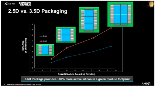
Source: AMD, Nomura research
Fig. 261: Floorplan of AMD MI455 and cross section
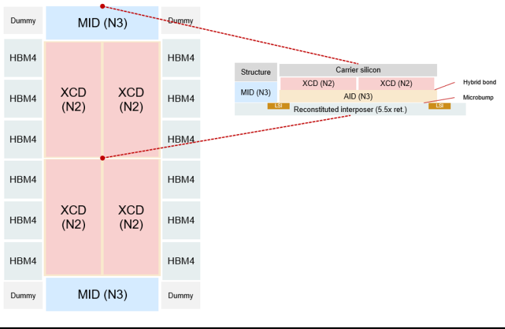
Source: Company data, Nomura research
Face
Face
Carrier silicon -> SiC (?)
GPU die (A16?)
GPU die (A167)
Reconstituted interposer (6-7x ret.)
Face to Face
7x available signal connections through HCB
Shorter signal routing, higher performance
High fleeblity to spit ASIC architecture between top & bottom dies
1 BROADCOM
Fig. 260: Broadcom introduced face-to-face 3D hybrid bond on its 3.5D platform
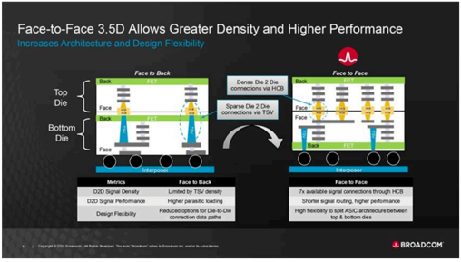
Source: Broadcom, Nomura research
Fig. 262: The floor plan and cross-section chart of nVidia's Feynman GPU
SiC thermal plate to function as an intergrated silicon carrier (fill up the height gap in between GPU and HBM) and thermal interface material (TIM)
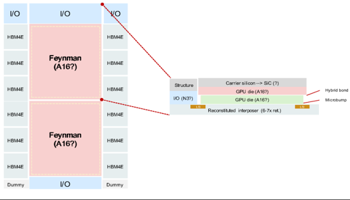
Source: Company data, Nomura estimates
Face to Face
Hybrid bond
Microbump
7,500
6,000
4,500
3,000
1,500
0
Fig. 263: TDP of nVidia products
6kW?
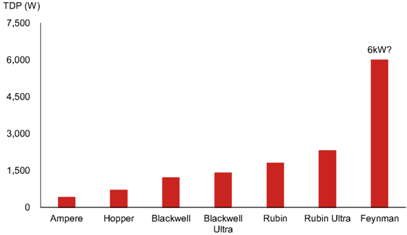
Source: Company data, Nomura estimates
Continued CoWoS capacity growth at TSMC, fueled by AI/HPC
We think TSMC's CoWoS capacity growth is one proxy (albeit imperfect) for Chroma's SLT handler sales volume trend as both are primarily fueled by AI/HPC demand, and Chroma's key SLT handler customers nVidia and AMD (starting from MI400-series) together could consume about 65% of CoWoS capacity each year, as per our estimates. We also estimate that c.70% of Chroma's Semiconductor/Photonic test revenue comes from AI/HPC in 2026F. But, we note that there is not necessarily a mathematical relationship between CoWoS capacity builds and handler purchases given varying output per interposer wafer for different AI accelerators and the throughput factor in handlers.
We do admit that one caveat of using the CoWoS capacity growth to sketch the growth trajectory of Chroma's AI SLT handler business is that SLT is not yet a mandatory stage during the semiconductor backend process. However, traditional ATE-driven FT alone may be no longer sufficient to detect all structural and functional defects since logic chip packages become more complicated, and from a structural standpoint, we foresee more ubiquitous adoption of SLT going forward, particularly for AI chips whose field returns could be extremely costly. These secular tailwinds are clearly beneficial for leading AI SLT handlers like Chroma, in our view.
To date, TSMC's supply is apparently still constrained across the front-end and the backend given the demand strength from AI, and the company has expressed its commitment to expand its capacity in due course, citing that it 'works very hard to meet all the demand ' and 'doesn't leave any business on the table ' (see remarks from 4Q25 and 1Q26 results ). We observe TSMC has turned more aggressive on CoWoS capacity planning (or more precisely, 'CoW' capacity) in recent months in response to surging AI chip demand, and lifted the capex guidance again in the July earnings call (report ), which should indirectly underscore the growth trajectory of Chroma's SLT handler business.
In our most recent Asia AI Semi & Server Anchor Report , our supply chain survey suggests TSMC will likely expand its CoWoS capacity to 1,100kpcs in 2026F (or c.130kwpm by the end of 2026F) and bring this up to 2,000kpcs in 2027F. Although TSMC has turned more aggressive in its CoWoS plan, our contrarian view is that 'WoS' (not controlled by TSMC) and many small components (e.g. IC substrates) would very likely become a bigger bottleneck than 'CoW' (controlled by TSMC) in 2027F. We only model 1,800kpcs of CoWoS output in 2027F (despite our assumption of a TSMC target of 2,000kpcs).
While we have no clear bottom-up estimates about how TSMC is going to expand its CoWoS capacity beyond 2027F, we had tried to triangulate a possible trajectory in our Asia AI Semi & Sever Anchor Report , based on TSMC's AI semi growth guidance and our assumptions of manufacturing content added. TSMC's guidance might hint to form 2,500-3,500kpcs of annual CoWoS capacity by 2029F, vs 680kpcs in 2025, and this would suggest a 40-50% capacity CAGR over 2025-29F compared to a >80% CAGR
(kpcs)
2,000
(kpcs)
600
1,500
500
400
1,000
300
500
200
100
0
0
(kpcs)
2,000
100%
planned for 2022-27E. If the expansion track prevails, we believe Chroma's AI SLT handler sales could continue to benefit from associated backend testing capex investments by TSMC and its ecosystem partners beyond 2027F.
40%
20%
500
0%
0
Source: Company data, Nomura estimates
Fig. 265: But the output will be constrained by "WoS"
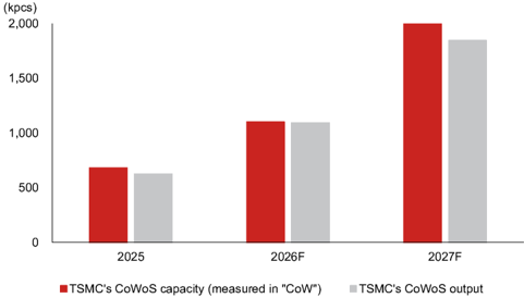
Source: Company data, Nomura estimates
Fig. 267: TSMC's CoWoS output allocation
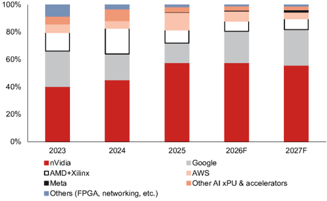
Fig. 264: TSMC turning more aggressive on CoW capacity expansion
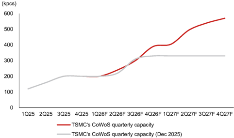
2023
•nVidia
DAMD+Xilinx
• Meta
Source: Company data, Nomura estimates
Fig. 266: TSMC's CoWoS output breakdown
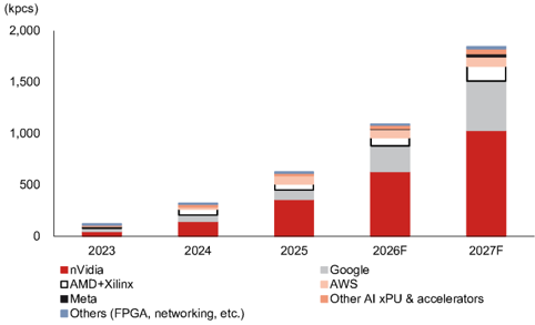
Source: Company data, Nomura estimates
Source: Company data, Nomura estimates
Emerging OSATs' 2.5D engagements bode well for Chroma in the long run
We believe that more 2.5D/CoW engagements and capacity additions by OSATs could be long-term volume catalysts for Chroma's SLT handler business, aside from TSMC's expansion, if SLT gradually becomes an indispensable norm for compute chips. We first wrote about TSMC's prudent approach to CoW capacity expansion in our Asia AI Semi & Server Anchor report in August 2025 , and noted that such planning was critical for OSATs as it had driven most AI chip customers to look for alternative CoW suppliers. We estimate ASE (3711 TT, Buy) could form 25kwpm of FOCoS capacity by end-2026F, from 5kwpm installed by end-2025.
Amkor (AMKR US, Not rated) is also an alternate CoW partner, and management highlighted over a dozen 2.5D engagements (silicon interposer-based, as per Amkor's definition) and expected high-density fan-out RDL devices (i.e., organic interposer-based) ramping up production in 2026E and bridge-type solution for AMD in 2027E (see Amkor's Investor Day 2026 ). Our industry checks suggest Amkor might have c.15kwpm of 2.5D/SWIFT capacity by end-2026F.
Despite many 2.5D/molded interposer-based packages in the pipeline of OSATs are for CPUs owing to more relaxed technological requirements (e.g., RDL line/space) and the absence of expensive HBM content (report ), those chip packages are naturally more complicated than conventional FCBGA and could prolong the testing time.
2024
2025
2026F
2027F
Fig. 268: 2.5D advanced packaging solution comparison
| 2.5D chip-last | TSMC | Intel Foundry | Samsung Foundry | ASE | SPIL | Amkor | Powertech |
|---|---|---|---|---|---|---|---|
| Silicon/TSV interposer | CoWoS-S (~3.3x ret.) | Foveros-S (~4x ret.) | I-CubeS H-Cube | 2.5D | 2.5D | 2.5D | 2.5D |
| Fan-out RDL | CoWoS-R (~5.5x ret.) | Foveros-R (production in 2027E) | n.a. | FOCoS | FO-MCM | S-SWIFT | CLIP (PLP) |
| Fan-out bridge (embedded in RDL) | CoWoS-L (>14x ret. by 2029E) | Foveros-B (production in 2027E) | I-CubeE | FOCoS-B | FO-EB | S-Connect | PiFO (PLP) (~9x ret. by 2028E) |
| Fan-out bridge (embedded in IC substrate) | - | EMIB (>12x ret. by 2028E) | - | - | - | - | - |
Source: Company data, Nomura research
Fig. 269: Major CoW projects at OSATs
| Fan-out RDL | Fan-out bridge | |
|---|---|---|
| ASE/SPIL | AMD Medusa? | AMD Venice |
| Amkor | nVidia GB10 nVidia Vera Microsoft Cobalt 200 | AMD Venice? (2027E) |
| Powertech | AMD Medusa? (PLP) | AMD's next gen? (PLP) |
Source: Company data, Nomura research
Google Axion CPU - a new SLT opportunity for Chroma
One example of potentially more SLT adoption is Google's own Axion CPU lineup, and a new demand driver for Chroma's equipment regime. We wrote in our December 2025 Asia AI Semi & Server report that we observed that an increasing number of CSPs were developing their own ASIC CPUs for AI assistance purposes, in addition to the typical x86 CPU general servers. We believe the trend is not at recess currently (and likely will not). The head node CPU amount paired with accelerators has been widely discussed after Google released its latest TPU v8t/v8i in late April 2026. The company specially mentioned that it has doubled the CPU usage per server, and it has increased adoption of in-house Axion CPUs - previously this was usually paired with x86 CPUs.
We had flagged demand upside from Google's ARM-based CPU 'Axion N4A' (on TSMC 3nm; codenamed 'Cypress') to the Asia supply chain in August and December last year, which in part is driven by the CPU adoption shift in the latest TPU 8t/8i from x86-based to Google Axion. We believe the supply chain logistics of Axion N4A are handled by GUC (3443 TT, Neutral), and KYEC (2449 TT, Buy) supports the FT stage using Advantest's ATE paired with Hon's ATC/handler, and the SLT stage using Chroma's handler . The current project in production has a monolithic layout, but our industry checks suggest the next generation may be a dual-die configuration, still utilizing FCBGA package, for releases in 2028F.
We argue that chiplet-based or multi-die floor plans will trade monolithic simplicity for a highly complex testing paradigm to validate die-to-die interconnect efficiency at longer testing time. Moreover, the multi-die layout naturally distributes the thermal load across the package and hence poses an intricate thermal management challenge to the SLT handlers. The system must deploy ultra-precise, multi-zone active thermal heads to dynamically balance the wildly mismatched self-heating conditions across dies to prevent inflicting thermal damages on the chip package. Chroma, in our view, possesses unique ATC capabilities to stand out as early as the engineering phases.
nVidia
AMD
AWS
Microsoft
Arm
Olympus core
Fig. 270: An overview of CPU layout
?
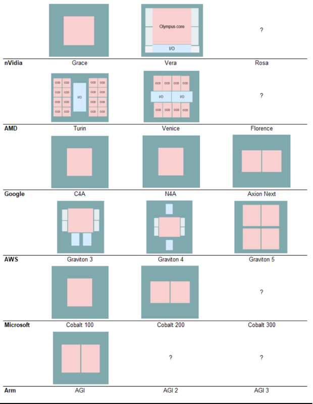
Source: Company data, Nomura estimates
Chroma to benefit from increasing testing spending by AI OSATs
We expect Chroma's ATC/handler business to benefit from an increase in testing capex by AI OSATs as large package footprints remain the pillar of AI accelerators, and OSATs are aggressively adding floor space and tester capacity in response to the considerable surge in total test time per devices. We compile capex plans and estimates by major OSATs with testing service exposures to North American AI chip customers, which are poised to jump in 2026-27F. Although some of them do not break down spending budgets in terms of assembly and test; directionally, we expect higher dollar spent on testing, with potential upside contemplating TSMC's more aggressive CoWoS expansion plans and OSATs' participation in the full 2.5D turnkey. Meanwhile, SEMI also projects global test equipment spending to record a c.20% CAGR over 2025-28E. We believe all these should point to a robust SLT handler growth trend for Chroma through 2028F. For nearterm trajectory, we compare Chroma's semi/photonics test revenue patterns to leadingedge SoC tester TAM projections provided by Advantest and Teradyne as well, despite no perfect numerical relationship between tester sales and SLT handler sales, which both suggest a robust y-y business growth in 2026F.
36
12,500
30
10,000
24
7,500
18
12
5,000
6
2,500đ
0
0
Fig. 271: AI OSAT capex trend
2022
2019
Courca: Comnany dota Plasmhara Cinancal D Mamura astimataa
36
30
20
24
15
18
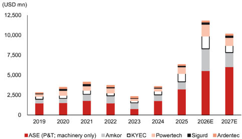
Source: Company data, Bloomberg Finance LP, Nomura estimates
Fig. 273: Chroma's revenue vs. SoC tester TAM estimates by Advantest
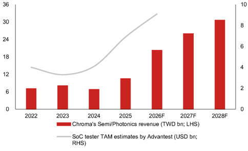
Source: Company data, Nomura estimates
10
8
6
Fig. 272: Increasing test equipment spending
2022
2015 2016 2017 2018 2019 2020 2021|
10
40%
8
20%
6
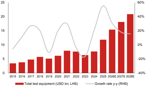
Source: SEMI, Nomura research
Fig. 274: Chroma's revenue vs. SoC tester TAM estimates by Teradyne
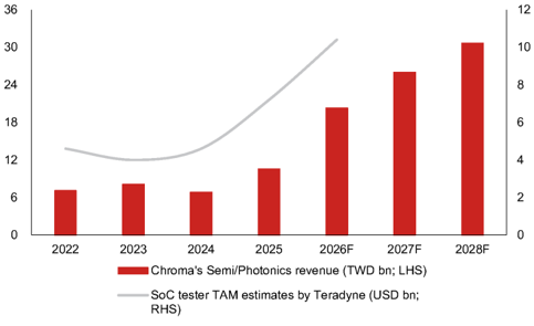
Note: Teradyne has not yet broken down its ATE TAM of USD12-14bn in 2026E. We assume 80% of the TAM comes from SoC testers based on historical patterns. Source: Company data, Nomura estimates
Moving up the manufacturing chain with metrology tools
Although Chroma's semiconductor test solutions have historically focused on the back end of the manufacturing flows (i.e., FT and SLT), the company has attempted to move up the value chain and tap into wafer-level metrology with Model 7980 and Model 7981, feasting on growing advanced packaging demand. We note that Model 7980 is used to inspect the microscopic impressions left on a wafer's bond pads by electrical test probes after CP, and Model 7981 runs measurement and inspection of redistribution layer (RDL) key dimensions (layer thickness, in our view), which becomes more challenging due to process variation, multi-layer build-up and finer metal interconnects. Both systems utilize Chroma's proprietary broadband light interferometry system (BLiS) to achieve 2D/3D nanoscale nondestructive optical measurement.
We believe both systems will tag along with TSMC's and OSATs' 2.5D/CoWoS capacity expansion. For Model 7980 specifically, we reckon a major demand driver could be TSMC's outsourcing of CP to OSAT partners such as KYEC which have to build up corresponding CP capacity (and therefore probe mark metrology lines). Chiplet-based designs also compound CP testing intensity for subsequent known good die assembly, and more CP cycles might further ignite demand for Chroma's Model 7980, in our view. As far as Model 7981, we view the trend toward more layers of RDL build-up in AI/HPC chips for stronger performance an incremental positive (AI/HPC's layer count is typically more than five), and the adoption of chip-last WMCM in mobile application processors may relax natural layer constraints for future upgrades (InFO-PoP has 3L of RDL, and the first-generation WMCM also features 3L). Additionally, Chroma is working on the
7980
2D/3D Metrology Measurement System
2D/3D Metrology Measurement System development of new wafer-level metrology tools to prepare for the roll-out of CoPoS, whose form factor change will result in another round of equipment upgrades, in our view, due to different inspection aspects for panel carrier vs. round carrier.
Chip
HBM
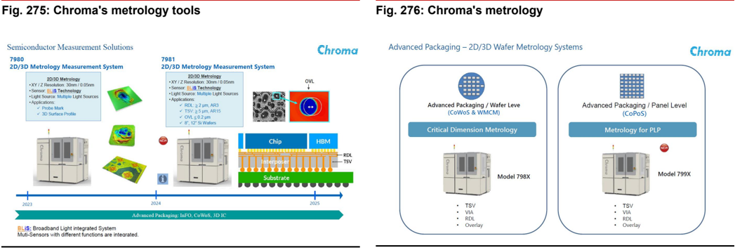
2023
BLiS: Broadband Light integrated System
Muti-Sensors with different functions are interated.
Source: Company data, Nomura research
New opportunity from CPO test insertions
We expect photonic testing in CPO to be an additional long-term growth catalyst for Chroma's Semiconductor/Photonic Test business, and Chroma's test handlers will likely play a role in test insertion 3 for validating optical engines (OEs) after die singulation and receptacle attach, which is a sheer optical test (O/O test). We view Chroma's established experiences in photonics, through LED, VCSEL (e.g., 3D sensing), and CMOS image sensor reliability testing, as a structural advantage paving the way for test insertion 3, where optical properties become the most critical yield determinants. Interestingly, from our industry surveys, there are two variants of test insertion 3 under development, implying no uniform standard for the flow at the moment. One of the approaches test the OE directly, whereas the other is a post-assembly O/O test after a fiber array unit (FAU) or a receptacle is attached onto the OE.
Chroma's experience in photonics could also grant Chroma a ticket to participate in test insertion 4 (validation of a CPO module housing switch ASIC and OEs). In this phase, we believe Chroma will be shipping an O/O tester for external laser source reliability before SLT. Meanwhile, Chroma is also developing wafer-level tester solution for photonic IC wafers (i.e. insertion 1).
Any undetected defect in a single optical component would force manufacturers to scrap an entire expensive CPO switch module, and therefore testing cannot wait until final assembly. Strategically inserting tests early to validate known good optical/electrical dies and inspecting packages is the only way to manage the intense thermal-mechanical vulnerability of CPO and ensure viable manufacturing yield. As far as we know,, there are currently four test insertions during CPO production by TSMC and its ecosystem partners, with two occurring under the scrutiny of TSMC and the subsequent two occurring at the OSATs. We take a deep dive into test insertions in our Anchor Report.
Our current expectation is Chroma will play a role in CPO test insertion 3 and insertion 4, but out model assumption only considers Chroma to begin small volume tool shipments in 2027F. Ramp-up timeline of CPO remains an uncertainty to us, and we will closely monitor the fluid supply chain dynamics. Any faster progress in the technology deployment could present upsides to Chroma's earnings beyond 2028F, in our view.
Chroma
Advanced Packaging - 2D/3D Wafer Metrology Systems
Advanced Packaging / Panel Level
(CoPoS)
Metrology for PLP
Source: Company data, Nomura research
Insertion 2
Fig. 277: CPO insertion flow and potential suppliers
EPIC wafer-level test
Insertion 3
Chroma
CPO Switch
ДЫМЫЫЫЫ
Silicon
EIC Silicon
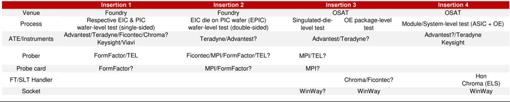
| Insertion 1 | Insertion 2 | Insertion 3 | Insertion 3 | Insertion 4 | |
|---|---|---|---|---|---|
| Venue | Foundry | Foundry | OSAT | OSAT | OSAT |
| Process | Respective EIC & PIC wafer-level test (single-sided) | EIC die on PIC wafer (EPIC) wafer-level test (double-sided) | Singulated-die- level test | OE package-level test | Module/System-level test (ASIC + OE) |
| ATE/Instruments | Advantest/Teradyne/Ficontec/Chroma? Keysight/Viavi | Teradyne/Advantest? | Advantest/Teradyne? | Advantest/Teradyne? | Advantest?/Teradyne Keysight |
| Prober | FormFactor/TEL | Ficontec/MPI/FormFactor/TEL? | MPI/TEL? | ||
| Probe card | FormFactor? | MPI/FormFactor? | MPI? | ||
| FT/SLT Handler | Chroma/Ficontec? | Hon Chroma (ELS) | |||
| Socket | WinWay? | WinWay | WinWay |
Source: Nomura research
Optical Test
Reliability Test & WAT
• Electrical Test
Fig. 278: CPO insertion flow
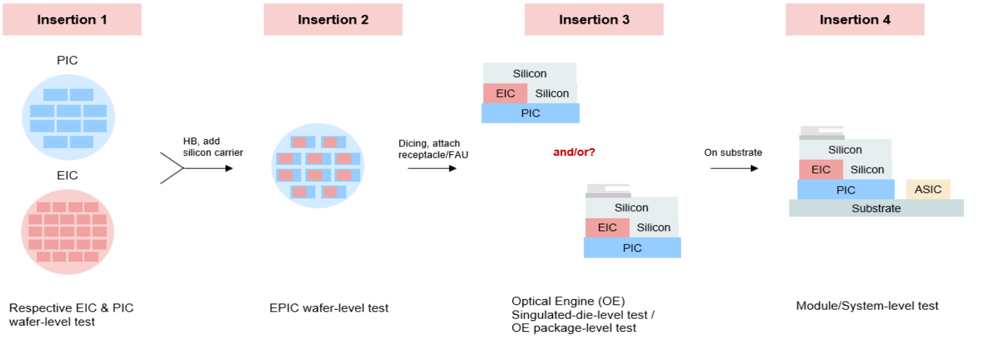
Note: This is a conceptual illustration, not specific to any company or project.
Source: Nomura research
Fig. 279: Chroma's solutions in CPO test insertions
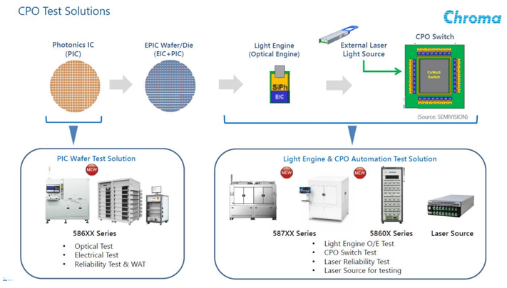
Source: Company data, Nomura research
587XX Series
Singulated-die-level test /
5860X Series
Laser Source
Light Engine O/E Test
OE package-level test
CPO Switch Test
Laser Reliability Test
Laser Source for testing
Insertion 4
Module/System-level test
60,000
50,000
40,000
30,000
20,000
10,000
0
(TWD mn)
35,000
ATS - fully charged in AI server power upgrades 20,000
We believe Chroma is well positioned to monetize the transition of the AI server power architecture moving from traditional ~50V DC intermediate bus voltage (IBV) toward HVDC (±400V or 800V) power racks in view of better energy efficiency. Chroma has 38% of its revenue from ATS in 2026F and provides test and measurement equipment to power supply makers such as Delta (2308 TT, Buy) and Lite-On (2301 TT, Buy) in order to build and qualify their next-generation 'powerhouses'. Chroma has comprehensive test solutions for server power supply units (PSUs), power shelves, power racks, and backup battery units (BBUs), and its product roadmap has moved in lockstep with the industry's HVDC development journey. We expect a multi-year, capex-linked revenue stream for Chroma rather than a one-off product upgrade cycle, and therefore estimate Chroma to grow its ATS revenue at a 43% CAGR over 2025-28F against our modeled capex for Delta and Lite-On where we see potential spending upside.
Fig. 280: Chroma's ATS revenue vs. Delta's capex
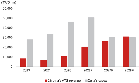
Source: Company data, Nomura estimates
AI power upgrade to HVDC is underway
Against the backdrop of rising power consumption and performance demand from AI chips, we believe the current mainstream power supply solution - 33kW and 72kW power shelves housed within IT racks and operating at 48-54V (~50V) DC as the IBV - is approaching its practical ceiling for further scale-up, constrained by rack space and rising energy losses. We believe AI racks running at TDP of 400kW and above will need to move toward standalone power racks , while racks operating at 750kW-1MW and above will require 800V HVDC power racks to sustain acceptable energy efficiency, given that 800VDC offers significantly lower current and lower energy vs 50VDC. We expect accelerating AI chip performance upgrades to drive HVDC power rack adoption by late 2026F-2027F, with some CSPs potentially moving even earlier to capture the energyefficiency and total cost of ownership (TCO) benefits. Please see our Asia AI Power Supply report in September 2025 for more comprehensive color on HVDC power rack upgrades.
For nVidia's AI GPU products, GB200 NVL36 and GB300 NVL72 racks, respectively consume 130-150kW and 180-200kW per rack, and each is predominantly powered by 4 and 6 layers of 33kW 1U power shelves (based on 54V PSU, each supplying 5.5kW) with the rack. Some GB300 NVL72 configurations instead use 3-4 layers of 72kW 1U power shelves (based on 54V PSU, each supplying 12kW).
The baseline model of upcoming VR200 NVL72 rack, in our view, may draw 220kW per rack. Without a standalone power sidecar, we think the rack could be powered by 2-4 layers of 110kW 3U power shelves factoring in power redundancy, and the power shelf is built on 54V PSU, each supplying 18.3kW. The other available option is equipping the rack with 4-5 layers of 72kW 1U power shelves (based on 54V PSU, each supplying 12kW).
Despite a compromised chip floor plan for Rubin Ultra (i.e., from four GPU dies in a
2026F
2027F
•Lite-On's capex
Fig. 281: Chroma's ATS revenue vs. Lite-On's capex
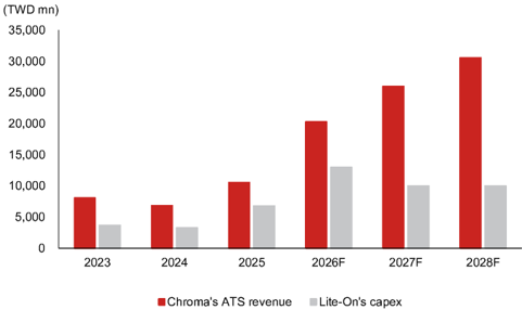
Source: Company data, Nomura estimates
2028F
package to two dies, similar to Rubin) and a likely production bottleneck with the Kyber architecture of higher compute density than the current Oberon, the TDP growth trajectory of the nVidia AI platform remains directionally intact, in our view. We may not witness a massive TDP leap in Rubin Ultra, but the Feynman platform (scheduled for 2028E) could be a node that sharply inflects up, considering the aggressive GPU-on-GPU SoIC stacking proposed on the chip end together with possible concurrent upgrades in other power-hungry interconnecting components. When the platform roadmap gradually unfolds even closer to 1MW per rack, only 800V HVDC power rack could adequately support the power requirement.
Delta is en route to ±400VDC shipments from 2H26F for a top US CSP
We are aware of recent concerns in the investment community about slower-thanexpected HVDC adoption and a setback for the power supply architecture transition, with some only recognizing 800VDC as 'the real HVDC'. Nevertheless, we argue the perception is biased and have been holding the view that ±400VDC adoption will kick off first, whereas the 800VDC timeline is subject to safety certifications , and that ± 400VDC is not a detour from 800VDC. We believe the adoption trajectory remains intact, and a top US CSP is en route to ±400VDC adoption from 2H26F with power sidecars supplied by Delta, likely beginning with VR200 racks before extending the architecture to its own ASIC racks. We expect Chroma to be a key test instrument supplier to Delta and is hence poised to benefit from ±400VDC moving from qualification toward volume production.
We would also note that the ±400VDC racks require BBU and capacitor bank units (CBUs) , both adding complexity to the rack architecture and the associated test requirements. The addition of BBU and CBU, in our view, suggest an extension of test coverage beyond the core power rack conversion path to include also backup power and transient energy buffering validation, thereby layering incremental test content and complexity onto an already-expanding HVDC test scope. This could present a tailwind to Chroma, with product breadth spanning across power, battery and rack-level instrumentation.
Even without HVDC, more power shelves also complicate testing efforts
In the worst case, if there are no signs of HVDC adoption in the upcoming VR200, the rack would still require more trays of PSUs to support the higher power level, and the testing complexity would therefore rise in tandem with shelf counts, in our view. Based on the aforementioned discussions about specs, the VR200 NVL72 would need a total of 612 x 18.3kW/4-5x 72kW PSU trays vs 6x 5.5kW/3-4x 72kW PSU trays in the GB300 NVL72. We reason that every additional power shelf layer introduces more parallel current-sharing paths and more interconnects that must be validated both independently and in aggregate under real load conditions. As a result, testing equipment has to handle more current, and engineers must verify that multiple PSUs can share load and stay in sync. More sophisticated testing efforts, in our view, remain a secular positive for Chroma.
The HVDC power evolution does not simply stop at 800V, with SST emerging
We view the solid state transformer (SST) as the next-generation architecture for HVDC power delivery in AI data centers. SST directly converts medium-voltage AC (MVAC, 10kV to 34.5kV utility-grade electricity) into HVDC distribution voltages (±400V or 800V) and integrates the traditional MV transformer and HVDC conversion functions into one unified stop. By consolidating what has historically been a multi-stage conversion process into fewer steps, SST significantly reduces cumulative power conversion losses, since the aggregate efficiency loss along the grid-to-chip power path decreases when the conversion stages decrease. We have an illustration of the SST-based pathway as Path E in Fig. 282 .
omura | Advanced Semi Testing
Fig. 282: Overview of power architecture in data center
Fig. 282: Overview of power architecture in data center
310 KV /133 KV 120 KO
Utility MV Grid
ON 0 N/204
AC
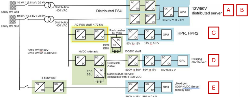
Utility MV Grid
Source: Delta, Nomura Research
Source: Delta, Nomura Research
Beyond efficiency, we see SST as a structural enabler of the broader shift toward carbonneutral data center design. A key architectural advantage is that SST power conversion is bidirectional . Traditional passive transformers rely on electromagnetic induction between primary and secondary coils (or windings) around a shared magnetic core to step voltage up or down with no active control over power flow direction (i.e., unidirectional). By contrast, an SST is built from a cascade of active power electronic stages using semiconductor switches (e.g., SiC or GaN-based for high-frequency switching) rather than passive magnetic coupling. The circuit topology typically starts with AC/DC rectification, followed by a high-frequency isolated DC/DC that steps voltage down to HVDC distribution levels, and with an optional DC/AC stage for grid-interactive applications . Because power flow direction is controllable at each active stage, the overall SST can support energy flow both from grid to storage (charging up BBUs during normal operation), and from storage back to load or grid (discharging during peak demand or grid instability) and offer an essential capability for micro-grid functionality rather than simple backup power.
Paired with energy storage systems (ESS) primarily consisting of BBUs, the bidirectional SST architecture can facilitate micro-grid integration, allowing data centers to buffer, store, and dispatch power more flexibly while smoothing grid demand and improving overall resilience. This SST+ESS combination could become a critical enabler for futuregeneration AI data centers, particularly as server rack loads scale to 1MW or higher, where consolidating grid-to-chip efficiency and scalability becomes essential to sustain both performance and power economies at scale.
More complicated power electronic testing moving to HVDC and SST
We reckon that AI server's shift toward 800V HVDC could reshape the entire test and measurement stack, as the current DC test regime is on the component level with unidirectional power supply, and electronic loads, power analyzers, and safety standards are all optimized for low-voltage (~50V), high-current profiles. However, when at 800V, we think the test instrumentation has to undergo structural reform because a substantially higher voltage changes insulation, creepage/clearance, and safety requirements in every test interface. Additionally, bidirectional power flows between grid, storage and load (notably SST) may need test equipment that can perform the role of source and sink vs. conventional one-way power supply. Much higher power drain by the rack could also spur the move from bench instruments to rack-scale test infrastructure.
We note that a few specific parameters become more crucial under the HVDC domain:
- Slew rate: Slew rate is how fast a voltage or current can change, and has become ·
Distribution
24 J
Phase more important in HVDC test become AI/HPC workloads create extremely fast, largemagnitude load steps (e.g. kilowatts within microseconds). The test system must be capable of ramping up the loads quickly to detect and validate the HVDC bus for transient response, droop, and recovery without triggering instability.
- Regenerative testing: Instead of dissipating test energy as heat through resistive loads, regenerative electronic loads sink power and feed it back to the grid. Regenerative testing is becoming more standard at multi-hundred-kW test power levels, both for facility thermal load management and for energy cost savings during high-volume production testing. · 3P 800VLN Re-generative Load · Max. 1200VDc.
1.44MW+
- BBU testing: BBUs will play a strategically more important role in HVDC racks, which support more power-hungry AI racks that cannot bear the loss from transient load swings or grid interruptions. BBUs can provide short-term localized power backup during power interruptions, and current BBUs are mainly operated at 12V and 54V for data center systems. For HVDC, BBU needs to support 800V, usually through series connection of batteries. Individual cell requires its own voltage-monitoring and balancing circuit, and thus more cells suggest more validation efforts. Moreover, BBUs must support rapid bidirectional charge/discharge cycles in sync with rack-level power demand, adding transient response and synchronization testing vectors on top of standard capacity/cycle-time validation. ·
- Arc testing: An arc is an unwanted electrical discharge through the air when a circuit connection loosens under load, and lightning bolt is an example of arc. DC arcs are particularly hazardous since the current never crosses zero (according to the physical property) and DC arcs tend not to self-extinguish upon ignition, unlike AC. The arc risk increases drastically at 800V HVDC, and thus makes arc detection and fast fault interruption a critical safety protocol. ·
- Double pulse test for wide-bandgap devices: The migration to HVDC could accelerate SiC and GaN adoption in the conversion stages for better efficiency and faster switching at higher voltages. This, in turn, raises the bar for test equipment bandwidth to accurately measure switching loss and electromagnetic interference. ·
Fig. 283: SST and Chroma's power test solutions
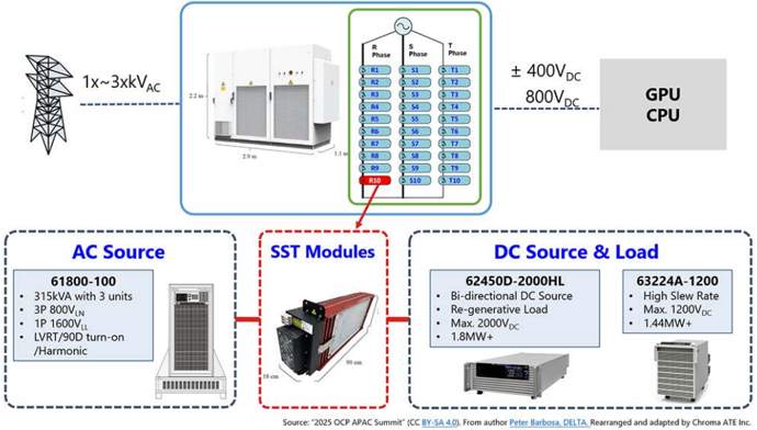
Source: Company data, Nomura research
Chroma leads in power electronics test instruments
The global electronic test and measurement market features five broader-line vendors: Keysight Technologies (KEYS US, Not rated), Rohde & Schwarz (unlisted), Tektronix (unlisted; a subsidiary of Ralliant [RAL US, Not rated]), National Instruments (unlisted; a subsidiary of Emersion [EMR US, Not rated]), and Anritsu (6754 JP, Neutral).
- Keysight is a general-purpose electronic test leader with the broadest portfolio, spanning RF/microwave, network and protocol test, semiconductor parametric test, ·
Model n1enn
• 10.kV
Power Supply Unit (PSU)
Battery Backup Unit (BBU)
and general-purpose power analysis/electronic loads.
Al Server Battery Backup Unit Test Solutions
Lithium-ion Batterv Cell
EDLC / LIC
- Rohde & Schwarz centers around RF/wireless, electromagnetic interference and compatibility (EMI/EMC), and automotive/aerospace communications test. · Battery pack
ATS
Battery Backup Unit (BBU)
konnnn
Capacitor Module
Power Capacitor Shelf (PCS)
Battery Pack BMS
Regenerative
- Tektronix's core is oscilloscopes, mixed-signal and power electronics analysis tools, across aerospace/defense, automotive, and renewable energy applications. ·
inn.enn.
- National Instruments has a solid foothold in modular, software-defined instrumentation and highly customizable automated test systems, addressing mostly semiconductor production test. · · CUKVA · 2KW - 24kW| 850y 0 - 540A tk=4.kWuoto.00k
- Anristu anchors its core to RF/microwave and optical communications test. ·
Chroma occupies a distinct niche relative to the top five vendors, and its portfolio centers around power electronics and batteries. The divergence from the global top test and measurement instrument makers per se, in our view, is strategically a competitive advantage of Chroma. The company's relevance in the AI server realm comes specifically from its high-power electronic loads, regenerative test systems, and rack/power-shelflevel tester across a wide spectrum of power levels. We notice Chroma's differentiation is less on any single specs but more on the breadth of its power electronics/battery test offerings coupled with deep engineering in high-power, bidirectional/regenerative systems, as evidenced by its continuous platform expansion including introduction of a comprehensive SST module test portfolio covering AC-side simulation and DC-side load testing (news ).
Nevertheless, we think most peers in this niche power test space compete within a narrower slice of the value chain. Kikusui (6912 JP, Not rated), ITECH (unlisted), and B&K Precision (unlisted) are positioned mainly around genera-purpose power supplies and electronic loads, while Arbin (unlisted), Maccor (unlisted), Bitrode (unlisted), and Neware (unlisted) are dedicated to battery cyclers. Chroma, by contrast, supports power supplies, electronic loads, regenerative/bidirectional systems and battery test under a single roof. As such, customers could enjoy a one-stop shop for test instruments and systems at a lower integration risk and TCO, when they have to broaden the test scope across power electronics and battery in response to structural migration in server power architectures. The end-to-end capabilities on the full power test stack with proven engineering also better help customers progress with the technical development, in our view.
Fig. 284: Chroma's AI server power test solutions
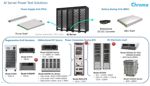
Source: Company data, Nomura research
Fig. 285: Chroma's solutions for AI server BBU test
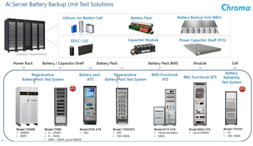
Source: Company data, Nomura research
Module
BMS Functional
ATS
Model 8710 ATS
540A
16cell simulator battery
Reliability
Test System
Model 17010H
5v t0ne 2ne
Chroma
Battery Pack
BBU Functional ATS
Model 8000 ATS
• Up to 500kW
80,000
60,000
40,000
20,000
0
MATS
Earnings forecasts
40,000
30,000
We expect a 45% net earnings CAGR over 2025-28F
We expect Chroma to grow its revenue by 89% y-y in 2026F on the back of 110% growth in Semiconductor/Photonics and 92% in ATS, driven by continued capacity expansion for the Asia AI OSAT supply chain and tool upgrades for nVidia's AI GPU platform refresh, and initial wave of HVDC adoption starting VR200 with more stringent power test requirements. Chroma's progress into 2D/3D wafer metrology could also capture another adjacency of advanced packaging capacity growth at TSMC and OSATs, in our view. We expect Chroma's revenue to witness a 49% CAGR over 2025-28F given structural testing trend for more complexity and longer time in AI/HPC chips (notably nVidia's planned adoption of GPU-on-GPU SoIC stacking for the Feynman platform), broader adoption of SLT, and sustained tool upgrades by power supply makers to foster the industry migration toward HVDC and SST.
The initial equipment opportunities from CPO test insertions (albeit likely small) might kick in from 2027F in the earliest, but we have not yet contemplated the contribution in our earnings estimates in detail, as the supply chain dynamics remain fluid, and we have to continue monitoring the development and viability of new technologies.
On the profitability front, we expect rather stable GM profiles across Chroma's major product lines, and believe equipment upgrades driven by power electronics and semiconductor testing are the predominant factors to the company's GM upswings. Our current assumptions reflect continued upgrade cycles along with AI/HPC and power electronics customers' roadmap primarily. We believe CPO test insertion tools could also be accretive to Chroma's GM in the longer run. We, hence, model GM of 62.4%/62.9%/63.7% in 2026-28F vs. 61.5% in 2025.
Blended in a 25% opex CAGR over 2025-28F, we anticipate Chroma to enjoy operating leverage from rapid topline expansion and grow its OPM to 46.3% in 2028F from 32.5% in 2025. Net, we estimate the company to deliver a 45% EPS CAGR over 2025-28F and think a successful ramp-up of CPO test insertion beyond 2028F could drive a more significant earnings upgrade.
Fig. 286: Chroma's revenue breakdown
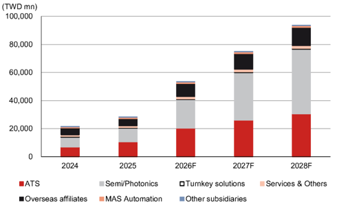
Source: Company data, Nomura estimates
Fig. 287: Chroma's net profit and y-y growth
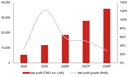
Source: Company data, Nomura estimates
2027F
2028F
• Net profit growth (RHS)
120%
100%
80%
60%
40%
20%
0%
Fig. 288: Chroma's P&L
| (TWD mn) | 1Q25 | 2Q25 | 3Q25 | 4Q25 | 1Q26 | 2Q26F | 3Q26F | 4Q26F | 1Q27F | 2Q27F | 3Q27F | 4Q27F | 2025 | 2026F | 2027F | 2028F |
|---|---|---|---|---|---|---|---|---|---|---|---|---|---|---|---|---|
| Revenue | 6,865 | 6,455 | 6,410 | 8,580 | 11,860 | 13,529 | 14,157 | 13,968 | 15,539 | 18,295 | 20,325 | 20,820 | 28,311 | 53,514 | 74,977 | 93,623 |
| Gross profit | 4,148 | 4,224 | 3,835 | 5,217 | 7,424 | 8,442 | 8,834 | 8,716 | 9,773 | 11,509 | 12,788 | 13,100 | 17,425 | 33,416 | 47,171 | 59,617 |
| - Opex | (1,984) | (2,027) | (1,987) | (2,229) | (2,627) | (2,706) | (2,831) | (2,794) | (2,875) | (3,293) | (3,618) | (3,706) | (8,227) | (10,957) | (13,491) | (16,232) |
| Operating profit | 2,164 | 2,197 | 1,848 | 2,988 | 4,797 | 5,736 | 6,003 | 5,922 | 6,899 | 8,216 | 9,170 | 9,394 | 9,198 | 22,458 | 33,680 | 43,385 |
| Pretax profit | 2,597 | 2,438 | 5,475 | 3,408 | 5,094 | 5,919 | 6,231 | 6,178 | 7,162 | 8,491 | 9,454 | 9,659 | 13,918 | 23,421 | 34,767 | 44,623 |
| Net profit | 2,122 | 1,953 | 5,066 | 2,550 | 3,864 | 4,708 | 4,966 | 4,932 | 5,719 | 6,784 | 7,555 | 7,720 | 11,692 | 18,471 | 27,778 | 35,687 |
| EPS (TWD) | 5.03 | 4.63 | 11.99 | 6.04 | 9.12 | 11.11 | 11.72 | 11.64 | 13.50 | 16.01 | 17.83 | 18.22 | 27.70 | 43.59 | 65.56 | 84.23 |
| Profitability | 1Q25 | 2Q25 | 3Q25 | 4Q25 | 1Q26 | 2Q26F | 3Q26F | 4Q26F | 1Q27F | 2Q27F | 3Q27F | 4Q27F | 2025 | 2026F | 2027F | 2028F |
| Gross margin | 60.4% | 65.4% | 59.8% | 60.8% | 62.6% | 62.4% | 62.4% | 62.4% | 62.9% | 62.9% | 62.9% | 62.9% | 61.5% | 62.4% | 62.9% | 63.7% |
| - Opex ratio | -28.9% | -31.4% | -31.0% | -26.0% | -22.1% | -20.0% | -20.0% | -20.0% | -18.5% | -18.0% | -17.8% | -17.8% | -29.1% | -20.5% | -18.0% | -17.3% |
| Operating margin | 31.5% | 34.0% | 28.8% | 34.8% | 40.5% | 42.4% | 42.4% | 42.4% | 44.4% | 44.9% | 45.1% | 45.1% | 32.5% | 42.0% | 44.9% | 46.3% |
| Pretax margin | 37.8% | 37.8% | 85.4% | 39.7% | 43.0% | 43.7% | 44.0% | 44.2% | 46.1% | 46.4% | 46.5% | 46.4% | 49.2% | 43.8% | 46.4% | 47.7% |
| Net margin | 30.9% | 30.3% | 79.0% | 29.7% | 32.6% | 34.8% | 35.1% | 35.3% | 36.8% | 37.1% | 37.2% | 37.1% | 41.3% | 34.5% | 37.0% | 38.1% |
| Q-Q | 1Q25 | 2Q25 | 3Q25 | 4Q25 | 1Q26 | 2Q26F | 3Q26F | 4Q26F | 1Q27F | 2Q27F | 3Q27F | 4Q27F | ||||
| Revenue | 13.7% | -6.0% | -0.7% | 33.9% | 38.2% | 14.1% | 4.6% | -1.3% | 11.2% | 17.7% | 11.1% | 2.4% | ||||
| Gross profit | 15.0% | 1.8% | -9.2% | 36.0% | 42.3% | 13.7% | 4.7% | -1.3% | 12.1% | 17.8% | 11.1% | 2.4% | ||||
| Operating profit | 38.8% | 1.5% | -15.9% | 61.7% | 60.6% | 19.6% | 4.7% | -1.3% | 16.5% | 19.1% | 11.6% | 2.4% | ||||
| Pretax profit | 33.9% | -6.1% | 124.5% | -37.8% | 49.5% | 16.2% | 5.3% | -0.8% | 15.9% | 18.6% | 11.3% | 2.2% | ||||
| Net profit | 43.8% | -8.0% | 159.4% | -49.7% | 51.5% | 21.8% | 5.5% | -0.7% | 16.0% | 18.6% | 11.4% | 2.2% | ||||
| Y-Y | 1Q25 | 2Q25 | 3Q25 | 4Q25 | 1Q26 | 2Q26F | 3Q26F | 4Q26F | 1Q27F | 2Q27F | 3Q27F | 4Q27F | 2025 | 2026F | 2027F | 2028F |
| Revenue | 55.4% | 17.1% | 13.8% | 42.1% | 72.8% | 109.6% | 120.9% | 62.8% | 31.0% | 35.2% | 43.6% | 49.1% | 31.0% | 89.0% | 40.1% | 24.9% |
| Gross profit | 61.6% | 29.3% | 16.0% | 44.6% | 79.0% | 99.8% | 130.3% | 67.1% | 31.6% | 36.3% | 44.8% | 50.3% | 36.7% | 91.8% | 41.2% | 26.4% |
| Operating profit | 140.3% | 45.1% | 22.5% | 91.6% | 121.7% | 161.0% | 224.8% | 98.2% | 43.8% | 43.2% | 52.8% | 58.6% | 67.8% | 144.2% | 50.0% | 28.8% |
| Pretax profit | 113.0% | 35.1% | 213.7% | 75.8% | 96.1% | 142.7% | 13.8% | 81.3% | 40.6% | 43.5% | 51.7% | 56.4% | 107.5% | 68.3% | 48.4% | 28.3% |
| Net profit | 122.2% | 38.8% | 255.3% | 72.8% | 82.1% | 141.1% | -2.0% | 93.4% | 48.0% | 44.1% | 52.1% | 56.5% | 122.1% | 58.0% | 50.4% | 28.5% |
Source: Company data, Nomura estimates
Fig. 289: Chroma: Segment revenue forecasts
| TWD mn | 2024 | 2025 | 2026F | 2027F | 2028F |
|---|---|---|---|---|---|
| Total revenue | 21,604 | 28,311 | 53,514 | 74,977 | 93,623 |
| y-y growth | 16% | 31% | 89% | 40% | 25% |
| Consolidated testing equipment business | 20,418 | 27,166 | 52,155 | 73,525 | 92,165 |
| y-y growth | 15% | 33% | 92% | 41% | 25% |
| MAS Automation | 873 | 884 | 1,096 | 1,190 | 1,195 |
| y-y growth | 32% | 1% | 24% | 9% | 0% |
| Other subsidiaries | 313 | 261 | 263 | 263 | 263 |
| y-y growth | 36% | -17% | 1% | 0% | 0% |
| Consolidated testing equipment business | |||||
| Parent | 15,651 | 22,012 | 42,892 | 62,425 | 79,245 |
| y-y growth | 25% | 41% | 95% | 46% | 27% |
| Test instruments & Automatic testing system (ATS) | 6,825 | 10,546 | 20,290 | 26,000 | 30,600 |
| y-y growth | -16% | 55% | 92% | 28% | 18% |
| Semiconductor/Photonics test solutions | 6,973 | 9,759 | 20,462 | 33,900 | 46,000 |
| y-y growth | 136% | 40% | 110% | 66% | 36% |
| Turnkey solutions | 685 | 444 | 448 | 520 | 580 |
| y-y growth | 51% | -35% | 1% | 16% | 12% |
| Services & Others | 1,168 | 1,263 | 1,692 | 2,005 | 2,065 |
| y-y growth | 13% | 8% | 34% | 18% | 3% |
| Overseas affiliates | 4,767 | 5,154 | 9,263 | 11,100 | 12,920 |
| y-y growth | -9% | 8% | 80% | 20% | 16% |
Source: Company data, Nomura estimates
Fig. 290: Nomura forecasts vs Bloomberg consensus for 2026-28F
| 2026F | 2026F | 2026F | 2027F | 2027F | 2027F | 2028F | 2028F | 2028F | |
|---|---|---|---|---|---|---|---|---|---|
| (TWD mn) | NMR | BBG | Diff. | NMR | BBG | Diff. | NMR | BBG | Diff. |
| Revenue | 53,514 | 52,164 | 2.6% | 74,977 | 73,834 | 1.5% | 93,623 | 88,504 | 5.8% |
| Gross profit | 33,416 | 32,946 | 1.4% | 47,171 | 47,127 | 0.1% | 59,617 | 55,613 | 7.2% |
| Operating profit | 22,458 | 21,443 | 4.7% | 33,680 | 33,611 | 0.2% | 43,385 | 45,708 | -5.1% |
| Pretax profit | 23,421 | 23,306 | 0.5% | 34,767 | 27,751 | 25.3% | 44,623 | 40,124 | 11.2% |
| Net profit | 18,471 | 18,088 | 2.1% | 27,778 | 27,975 | -0.7% | 35,687 | 32,713 | 9.1% |
| EPS (TWD) | 43.59 | 42.32 | 3.0% | 65.56 | 65.41 | 0.2% | 84.23 | 77.43 | 8.8% |
| Margin | NMR | BBG | Diff. | NMR | BBG | Diff. | NMR | BBG | Diff. |
| Gross margin | 62.4% | 63.2% | -71bps | 62.9% | 63.8% | -91bps | 63.7% | 62.8% | 84bps |
| Operating margin | 42.0% | 41.1% | 86bps | 44.9% | 45.5% | -60bps | 46.3% | 51.6% | -530bps |
| Pretax margin | 43.8% | 44.7% | -91bps | 46.4% | 37.6% | 878bps | 47.7% | 45.3% | 233bps |
| Net margin | 34.5% | 34.7% | -16bps | 37.0% | 37.9% | -84bps | 38.1% | 37.0% | 116bps |
Source: Bloomberg Finance L.P. consensus, Nomura estimates
70
40
30
20
10
Jul-21
25.0
Valuation methodology and risks
We derive our target price of TWD2,845, based on 38x average 2027-28F EPS of TWD74.9. Our target P/E multiple is at the higher end of Chroma's historical trading band of 14-58x, which we view reasonable given our modeled net earnings CAGR of 39% over 2026-28F. We believe the dual growth engines from Chroma's Semiconductor/Photonic Test and ATS, propelled by a myriad of margin-accretive catalysts such as SLT handler upgrades from more complicated merchant AI GPU designs, expanding SLT footprints in more AI/HPC customers, and the transition of AI server power architecture will continue to drive upsides to earnings. Although we do not factor in contribution from CPO test insertions, a successful ramp-up of CPO and associated test insertion adoption could drive further upgrades to earnings estimates beyond 2028F.
We select Chroma's valuation comparison peers from the semiconductor backend equipment and test interface vendor space, as well as players in data center power system and power system components, given its exposures to both fields. Chroma is currently trading at 32x 2027F EPS and 25x 2028F EPS, respectively, and we believe this is undemanding compared to average valuation of 39x by semiconductor backend equipment (specifically 37x by test equipment), 35x by test interface vendor, and 27x by data center power-related players (Chroma could have a higher valuation than pure power plays due to its exposure to semiconductor equipment, in our view), all based on consensus 2027E EPS.
Major downside risks to our call include: 1) CoWoS and backend testing capacity expansion slowdown; 2) slower-than-expected product refresh, platform performance upgrade, or ramp-up by the AI chip end customers; 3) fiercer-than-expected from other international testing equipment makers; and 4) weaker-than-expected end-market demand, particularly for AI servers.
Fig. 291: Chroma's consensus P/E ratio
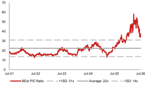
Source: Bloomberg Finance L.P., Nomura research
Fig. 292: Chroma's consensus P/B ratio
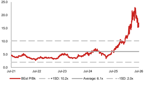
Source: Bloomberg Finance L.P., Nomura research
Jul-24
- Average: 6.1x
Jul-25
Jul-26
• - 1SD: 2.0x
3,100
2,600
2,100
1,600
1,100
600
100
Jul-21
Fig. 293: Valuation comparison of Chroma
122
102
82
6,000
5,000
4,000
2,500
2,000
| Last close | Target price | Upside (Downside) | Market Cap. | P/E (x) | P/B (x) | P/B (x) | P/B (x) | ROE | ROE | ROE | Dividend yield | Dividend yield | Dividend yield | |||||
|---|---|---|---|---|---|---|---|---|---|---|---|---|---|---|---|---|---|---|
| Ticker | Company Name | Rating | LCY | LCY | % | USD mn | FY26F | FY27F | FY28F | FY26F | FY27F | FY28F | FY26F | FY27F | FY28F | FY26F | FY27F | FY28F |
| Semi test equipment | ||||||||||||||||||
| 6857 JP | Advantest | Buy | 29,585.0 | 30,600.0 | 3 | 132,836 | 44.2 | 34.4 | 27.7 | 20.4 | 15.5 | 11.9 | 52.5% | 51.2% | 48.7% | 0.2% | 0.2% | 0.2% |
| TER US | Teradyne | Not rated | 374.0 | n.a. | n.a. | 58,553 | 51.1 | 37.2 | 26.7 | 16.2 | 13.1 | 10.0 | 37.5% | 41.7% | 41.9% | 0.1% | 0.1% | 0.2% |
| KEYS US | Keysight | Not rated | 328.1 | n.a. | n.a. | 56,072 | 32.2 | 27.6 | 24.6 | 8.2 | 6.8 | 5.6 | 25.9% | 26.4% | 26.1% | 0.0% | 0.0% | 0.0% |
| 7769 TT | Hon Precision | Buy | 6,405.0 | 11,100.0 | 73 | 35,597 | 47.7 | 29.3 | 19.0 | 16.3 | 12.4 | 9.1 | 37.6% | 48.1% | 55.3% | 1.5% | 2.4% | 3.7% |
| 300604 CH | Changchuan | Not rated | 309.1 | n.a. | n.a. | 28,944 | 94.5 | 64.3 | 46.8 | 29.3 | 20.5 | 14.5 | 33.4% | 34.7% | 33.7% | 0.1% | 0.2% | 0.2% |
| 2360 TT | Chroma | Buy | 2,125.0 | 2,845.0 | 34 | 27,912 | 48.7 | 32.4 | 25.2 | 21.3 | 15.7 | 12.3 | 49.8% | 55.8% | 54.6% | 1.4% | 2.2% | 2.8% |
| 688200 CH | Accotest | Not rated | 369.0 | n.a. | n.a. | 10,926 | 94.8 | 75.0 | 58.8 | 14.2 | 13.4 | 11.3 | 16.2% | 17.8% | 19.1% | 0.3% | 0.4% | 0.6% |
| COHU US | Cohu | Not rated | 56.2 | n.a. | n.a. | 2,652 | 95.8 | 38.3 | 26.4 | 3.5 | 3.2 | 2.9 | -207.6% | 27.2% | n.a. | n.a. | n.a. | n.a. |
| AEM SP | AEM | Not rated | 9.0 | n.a. | n.a. | 2,235 | 42.4 | 27.7 | 21.0 | 5.2 | 4.4 | 3.7 | 13.0% | 16.8% | 18.9% | 0.6% | 0.9% | 1.2% |
| 6337 JP | TESEC | Not rated | 2,339.0 | n.a. | n.a. | 80 | 20.3 | 18.8 | 16.3 | n.a. | n.a. | n.a. | n.a. | n.a. | n.a. | 4.3% | 4.3% | 4.3% |
| Average | 57.2 | 38.5 | 29.3 | 14.9 | 11.7 | 9.0 | ||||||||||||
| Semi test interface | ||||||||||||||||||
| TPRO IM | Technoprobe | Not rated | 31.2 | n.a. | n.a. | 22,854 | 71.9 | 47.2 | 37.0 | 13.2 | 10.5 | 8.3 | 19.6% | 22.6% | 23.1% | 0.0% | 0.1% | 0.2% |
| 6223 TT | MPI | Buy | 6,000.0 | 8,000.0 | 33 | 18,159 | 100.5 | 46.8 | 26.4 | 31.0 | 20.5 | 13.1 | 35.7% | 54.8% | 63.1% | 0.5% | 1.2% | 2.1% |
| FORM US | FormFactor | Not rated | 113.8 | n.a. | n.a. | 8,867 | 46.1 | 35.7 | 39.4 | n.a. | n.a. | n.a. | 15.4% | 18.7% | n.a. | 0.0% | 0.0% | n.a. |
| 6515 TT | WinWay | Buy | 6,500.0 | 8,315.0 | 28 | 7,235 | 73.6 | 35.0 | 19.5 | 32.7 | 20.6 | 12.8 | 46.4% | 71.6% | 80.4% | 1.0% | 2.2% | 3.9% |
| 6510 TT | CHPT | Suspended | 2,710.0 | n.a. | n.a. | 2,745 | 42.2 | 22.7 | 15.9 | 8.2 | 6.3 | n.a. | 20.8% | 31.8% | 56.0% | 1.3% | 2.3% | 2.9% |
| COHU US | Cohu | Not rated | 56.2 | n.a. | n.a. | 2,652 | 95.8 | 38.3 | 26.4 | 3.5 | 3.2 | 2.9 | -207.6% | 27.2% | n.a. | n.a. | n.a. | n.a. |
| 6941 JP | Yamaichi | Not rated | 9,380.0 | n.a. | n.a. | 1,181 | 17.6 | 15.7 | 13.7 | 3.2 | 2.8 | 2.4 | 19.3% | 20.4% | 20.7% | 1.7% | 1.8% | 2.1% |
| 6683 TT | KSMT | Not rated | 1,220.0 | n.a. | n.a. | 1,038 | n.a. | n.a. | n.a. | n.a. | n.a. | n.a. | n.a. | n.a. | n.a. | n.a. | n.a. | n.a. |
| Average | 64.0 | 34.5 | 25.5 | 15.3 | 10.6 | 7.9 | ||||||||||||
| AI OSAT | ||||||||||||||||||
| 3711 TT | ASE | Buy | 656.0 | 730.0 | 11 | 90,585 | 37.2 | 25.5 | 20.2 | 7.1 | 6.2 | 5.5 | 19.7% | 25.6% | 28.6% | 1.9% | 2.8% | 3.5% |
| AMKR US | Amkor | Not rated | 66.7 | n.a. | n.a. | 16,541 | 31.9 | 27.5 | 23.1 | 3.3 | 3.0 | 2.6 | 11.2% | 11.1% | 12.7% | 0.5% | 0.5% | 0.6% |
| 2449 TT | KYEC | Buy | 295.0 | 390.0 | 32 | 11,142 | 30.3 | 19.1 | 14.3 | 5.7 | 4.5 | 3.5 | 21.0% | 26.4% | 27.3% | 0.3% | 0.5% | 0.7% |
| 6239 TT | Powertech | Not rated | 294.0 | n.a. | n.a. | 6,894 | 24.5 | 16.9 | 15.0 | 3.4 | 3.0 | 2.7 | 15.7% | 18.8% | 18.6% | 2.4% | 3.3% | 3.7% |
| Average | 31.0 | 22.3 | 18.1 | 4.9 | 4.2 | 3.6 | ||||||||||||
| Datacenter power | ||||||||||||||||||
| SU FP | Schneider | Not rated | 268.8 | n.a. | n.a. | 177,387 | 27.2 | 23.2 | 20.2 | 5.7 | 5.0 | 4.4 | 21.3% | 22.2% | 22.4% | 1.7% | 1.9% | 2.1% |
| ETN US | Eaton | Not rated | 403.0 | n.a. | n.a. | 156,465 | 30.2 | 25.9 | 22.6 | 7.0 | 6.1 | 5.5 | 23.5% | 24.5% | 25.3% | 1.1% | 1.1% | 1.2% |
| 2308 TT | Delta | Buy | 1,880.0 | 2,800.0 | 49 | 150,838 | 44.6 | 27.8 | 20.1 | 14.6 | 10.7 | 8.0 | 36.3% | 44.4% | 45.5% | 1.1% | 1.8% | 2.5% |
| VRT US | Vertiv | Not rated | 304.5 | n.a. | n.a. | 116,961 | 47.0 | 36.0 | 28.0 | 19.7 | 13.8 | 9.7 | 48.8% | 46.4% | 42.8% | 0.1% | 0.1% | 0.2% |
| FLEX US | Flextronics | 127.4 | n.a. | n.a. | n.a. | |||||||||||||
| Not rated | n.a. | 46,674 | 28.7 | 18.7 | 13.7 | 8.2 | 6.6 | 4.3 | 32.2% | 43.6% | n.a. | n.a. | ||||||
| 2301 TT | Lite-On | Buy | 218.0 | 285.0 | 31 | 15,596 | 22.4 | 15.3 | 12.6 | 5.0 | 4.4 | n.a. | 23.4% | 30.5% 14.7% | 33.0% | 3.8% | 5.5% | n.a. |
| 002600 CH 002851 CH | Lead Wealth Megmeet | Not rated | 12.1 | n.a. | n.a. | 15,239 11,372 | 28.2 101.0 | 18.7 48.0 | 14.8 33.7 | n.a. 10.0 | 1.2 | 1.1 7.1 | 11.5% 10.5% | 17.9% | 16.3% 21.4% | 0.4% 0.1% | 0.7% 0.3% | 0.9% 0.4% |
| Average | Not rated | 131.7 | n.a. | n.a. | 41.2 | 26.7 | 20.7 | 10.0 | 8.5 7.0 | 5.7 |
Note: Priced as of 22 July 2026. Bloomberg consensus for Not rated and Rating Suspended stocks. Source: Company data, Bloomberg Finance L.P., Nomura estimates
Fig. 294: Chroma's share price vs. Bloomberg consensus EPS revisions
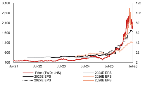
Source: Company data, Bloomberg Finance L.P. consensus estimates, Nomura research
Fig. 295: Chroma's share price vs. monthly revenue
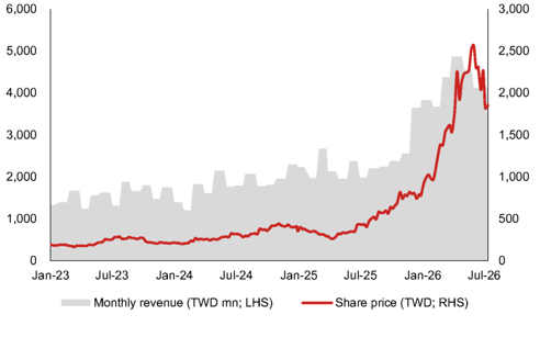
Source: Company data, TEJ, Nomura research
500
3,000
Fig. 296: Chroma's share price catalysts recap (2023-24)
2,000
300
1,500
200
1,000
100
500
0
Computex; positive market
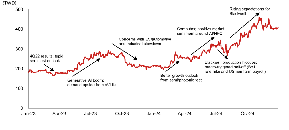
Source: Company data, TEJ, Nomura research
Fig. 297: Chroma's share price catalyst recap (2025-26 YTD)
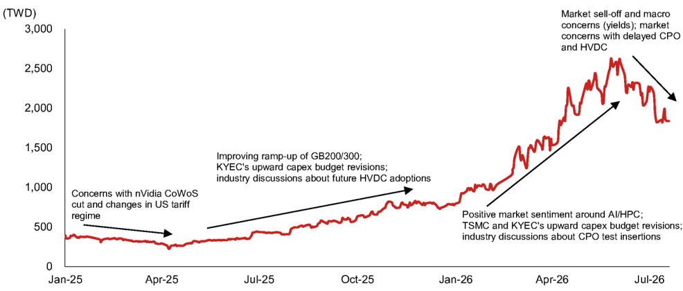
Source: Company data, TEJ, Nomura research
sentiment around Al/HPC
Market sell-off and macro concerns (yields); market
concerns with delayed CPO
Rising expectations for and HVDC
Blackwell
WW
Company background
Founded in 1984, Chroma ATE is a Taiwan-based supplier of precision electronic test and measurement instruments, automated test systems, intelligent manufacturing systems, and automation turnkey solutions. Chroma's primary production bases are concentrated in Taiwan, and it also operates assembly and module production footprints in China to support localized system integration. The company's end applications span sectors where precision quality control and reliable electro-optical performance are critical, including semiconductors, EV/renewable energy (e.g., battery cells), power electronics, specialized photonics, flat panel displays (FPD), and automated optical inspection systems.
More than 95% of Chroma's revenue comes from its testing equipment business, under which are test instruments and automatic testing systems (ATS), semiconductor/photonic tests, turnkey solutions, services and others, and overseas affiliates, and ~5% from its subsidiary MAS Automation.
- Test instrument & automatic testing systems (ATS; 37% of 2025 revenue): This segment covers testing equipment solutions for power supplies, battery cells, battery modules, electric drivetrains (e.g., battery storage systems, DC/DC converters), EV supply equipment (EVSE), etc. ·
- Semiconductor/Photonic tests (35% of 2025 revenue): Chroma's semiconductor testing equipment solutions address FT (tester and FT handler) and SLT (SLT handler). Chroma's SoC testers address a variety of mature-node chip applications including consumer electronics (MCU, audio, PC peripherals), PMIC, RF/wireless IC, and image sensors, and its FT handlers offer chip package pick-and-place automation and thermal control capabilities to work alongside testers. In SLT handlers, Chroma focuses on niche, quality-dependent applications such as AI/HPC and automotive to help customers verify their chips against simulated real-world conditions. The other part of this revenue segment is photonic test solutions for optoelectronic components (e.g., laser diode and LED), where Chroma offers both wafer level and package level test equipment. ·
- Overseas affiliates (22% of 2025 revenue): This segment contains Chroma's revenue booked through non-Taiwan entities. We think the application base is similar to that of ATS. ·
- Service and others (5% of 2025 revenue): Chroma books recurring aftermarket service revenues and are some smaller product lines like FPD test, video and color test under this segment. ·
- Turnkey solutions (3% of 2025 revenue): Chroma provides system-integration business bundling instruments, automations and software into complete productionline solutions. Sub-segments cover photovoltaics, battery formation and testing, and EV. The nature of the line is more customized and lumpier in revenue timing. ·
- MAS Automation (5% of 2025 revenue): This subsidiary involves in automation equipment for clean-energy manufacturing, such as photovoltaic equipment and lithium battery formation and grading equipment. ·
Chroma's business expansion has not been purely organic. Management has run a disciplined, phased M&A or equity investment program since the company was founded to convert the company from a standalone test instrument vendor to an integrated test, automation, and turnkey solution provider with progress into upstream semiconductor testing adjacencies.
In 2019, Chroma entered into an agreement with Camtek (CAMT US, Not rated), an Israeli semiconductor metrology and inspection equipment maker, to acquire 20.5% ownership. In addition to this investment, Chroma and Camtek entered into an agreement in which Camtek would license its triangulation technology for metrology to Chroma for non-semiconductor applications, and both parties agreed to cooperate in potential semiconductor equipment projects based on synergies between inspection and metrology technologies.
We summarize Chroma's development milestones and critical M&A history in Fig. 298 .
Fig. 298: Chroma's milestones and M&A history
| Year | Milestone and M&A history |
|---|---|
| 1984 | - Leo Huang, Chun-Sheng Chen, Ming-Hsiung Chang, and Hsiao-Hui Huang co- founded Chroma ATE Inc. and started developing measuring instruments, including the very first product "video pattern generator (VPG)" for monitor testing. |
| 1996 | - Chroma went public in Taiwan. |
| 1997 | - Invested in DynaScan Technology, a provider of high-brightness display solutions. |
| 1998 | - Invested in ADLINK Technology, an industrial PC maker. |
| 2000 | - Invested in EVT Technology. - Acquired Zentech Technology. |
| 2006 | - Spun off Special Material Business Unit and established a subsidiary "Chroma New Material" as the agency of Nippon Micrometal to sell bonding wire and micro solder ball for semi packages. |
| 2007 | - Acquired MAS Automation, an automation equipment supplier for solar modules and Li-ion batteries. - Acquired Sajet Technology, a smart manufacturing platform provider, and formed MES Business Unit. - Established a subsidiary "Testar Electronics", specialized in optoelectronic testing (LED, photodiode, VCSEL). |
| 2009 | - Acquired Raster Opto-Mechatronics, an optical measurement equipment maker. |
| 2011 | - Acquired Wise Life Technology, specialized in thermoelectric measurement systems. |
| 2012 | - Acquired QuadTech, a solution provider of electrical safety testers, passive component measurement testers, as well as AC and DC Power Sources, DC Loads and automation software. |
| 2013 | - Invested in ADIVIC Technology, a maker of RF measurement instruments. |
| 2016 | - Invested in Quantel Pte Ltd. as Chroma's Southeast Asia branch. |
| 2017 | - Established Innovative Nanotech, which builds nanoparticle monitoring systems for semiconductor manufacturing process control. - Invested in Touch Cloud, an AIoT solution provider. |
| 2019 | - Invested in Camtek, a global leading semiconductor metrology and inspection equipment vendor. - Formed Optical Inspection Solutions BU. |
| 2022 | - Acquired Environmental Stress Systems, whose main products consist of thermal forcing systems and could enable Chroma to grow the expertise in thermal control in semiconductor testing equipment. - Terminated Chroma New Material. |
Source: Company data, Nomura research
Fig. 299: Chroma's top shareholders
| Name | Ownership Remarks |
|---|---|
| Chun-Sheng Chen | 3.6% Co-founder Shu-Chuan Chen (spouse of Leo Huang) |
| Grandcrest Holdings Inc. | 3.5% is the representative; she also owns 1.01% of interest in Chroma. |
| Government of Singapore | 3.5% |
| Yu-Mei Hsueh | 2.6% Spouse of Chun-Sheng Chen |
| Leo Huang | 2.6% Chairman and co-founder |
| Labor Pension Fund | 2.3% |
| Yuanta/P-shares Taiwan Top 50 ETF | 1.7% |
| Norges Bank | 1.4% |
| Vanguard Total International Stock Index Fund | 1.2% |
| Vanguard Emerging Markets Stock Index Fund | 1.2% |
Note: Data as of May 2026.
Source: Company data, Nomura research
Others, 20.4%
Chun-Sheng Chen (co- investment vehicles), 7.1%
founder) and his family, 6.2%
Fig. 300: Chroma's shareholder structure
SITE, 6.7%
3,000
2,500
2,000
1,500
1,000
500
0
Jan-23
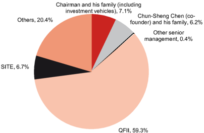
Note: Data as of 22 July 2026.
Source: Company data, TEJ, Nomura research
Fig. 302: Board of directors
| Position | Name | ownership Background |
|---|---|---|
| Chairperson | Leo Huang | 2.6% - Electronics Engineering Department, National Chiao Tung University - Co-founder and CEO of Chroma |
| Director | I-Shih Tseng | 0.1% - Ph.D in Mechanical Engineering, Pennsylvania State University - Manager, Institute for Information Industry - Deputy Chief Engineer of Chroma - General Manager of Chroma |
| Director | David Yang | 0.0% - Electronics Engineering Department, National Chiao Tung University - Deputy General Manager of Chroma - General Manager of Chroma |
| Director | David Huang | 0.8% - Business Administrative Commercial Study, University of Western Ontario - COO & Global Director of Business Development, DynaScan |
| Director | Shui-Yung Lin | 0.0% - Master from the Institute of International Taxation, Northrop University - Bachelor of Finance and Taxation, Feng Chia University - Chairman, Export-Import Bank of China - Commissioner of the Financial Affairs Department |
| Independent director | George Chen | 0.0% - Doctor of Atmospheric Science, State University of New York (Albany) - Academic Deputy General Manager of National Taiwan University - Deputy General Manager for Academic Affairs, National Taiwan University - Professor, Department of Atmospheric Sciences, National Taiwan University |
| Independent director | Jia-Ruey Duann | 0.0% - Ph.D in Physics from North Dakota State University - Harvard Business School Advanced Management Program - Assistant Deputy General Manager, ITRI - CEO, ITRI Southern Region Campus/ITRI Central Region Campus - Director of Measurement Technology Development Center, ITRI - Adjunct Professo, Department of Physics, Chung Yuan Christian University - President of Automatic Optical Inspection Equipment Association - Assistant Researcher of Precision Instrument Development Center, National |
| Independent director | Steven Wu | 0.0% - MBA, George Washington University Department of Industrial and Information Management, National Cheng Kung University - Senior Deputy General Manager, China Venture Management, Inc. - Senior Vice President, WI Harper Group - Deputy Manager, Investment Business Dept., Central Investment Holding Co., Ltd. - Assistant Manager, Investment Review Group, KMT Investment Business Management Committee - Senior Advisor, Corporate Financial Consulting Dept., Deloitte Taiwan - Investment Manager, DFV Fine Wines Group |
| Independent director | Janice Chang | 0.0% - Master of Business Administration, Major in Financial Management, Drexel University - Department of Accounting, National Chengchi University - VP, Capital Market Department, KGI Securities |
Note: Data as of May 2026.
Source: Company data, Nomura research
60%
Fig. 301: Chroma's share price vs. QFII and SITE ownerships
45%
30%
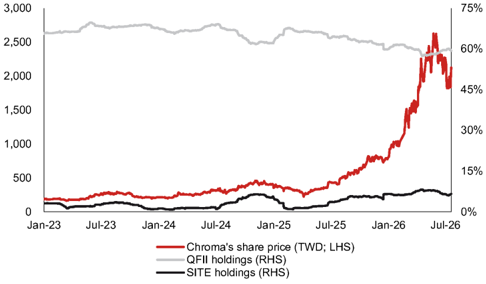
Note: Data as of 22 July 2026.
Source: TEJ, Nomura research
Rating and target price chart (three year history)
2750.00
2500.00
2250.00
2000.00
1750.00
1500.00
1250.00
1000.00
750.00
500.00
0.00
Chroma ATE Inc.
Appendix A-1
This report has been produced by Nomura International (Hong Kong) Ltd., Taipei Branch (NITB), Taiwan. See Disclaimers for Nomura Group entity details.