PDF 原檔:活動_穎崴_CPO論壇簡報_20260514_original.pdf
原始內容
Your Trusted Partner in Semiconductor Testing
The Evolution of Co-Packaged Optics (CPO) Advanced Testing Methodologies for Silicon Photonics Ai
Published Date 2026/05/14
Version v1.0
Presenter: Collins Sun
01
02
03
04
05
CPO and Test Flow
Bottleneck of Testing in CPO Production
CPO Roadmap & Trend
CPO/CPC Application
WinWay CPO/CPC Total Solution
Winkay
Tech
CPO and Test Flow
Winkay
Tech
Optical Industry M&A Wave in the AI Era
Nov 2024
Celestial AI acquires Rockley Photonics IP
Feb 2025
Nokia acquires Infinera
May 2025
AMD acquires Enosemi
Optical networking & DCI $2.3B
Dec 2025
Marvell to acquire Celestial AI
Apr 2026
Credo to acquire DustPhotonics
Apr 2026
Marvell acquires Polariton Technologies
$5.5M
Optical scale-up for AI
SiPho PIC vertical integration $1.3B
Undisclosed
Plasmonics + SiPho modulation

Chipmakers & Hyperscalers Back Photonics
Oct 2024
Google Ventures et al.
- → Lightmatter
Oct 2024
Cisco • NVIDIA
- → Xscape Photonics
Dec 2024
AMD • Intel • NVIDIA
- → AyarLabs
IC Design (joint) → Optical I/O
CSP → Photonic Computing
CSP/Networking + IC → DWDM
Feb 2026
MediaTek
- → AyarLabs
Mar 2026
NVIDIA
- → Lumentum
Mar 2026
NVIDIA
- → Coherent
$90M
IC Design → Optical I/O
IC Design → Laser / SiPho
$2.0B
$2.0B
IC Design → Laser / Networking

No Single Company Can Solve These Problems
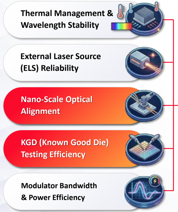
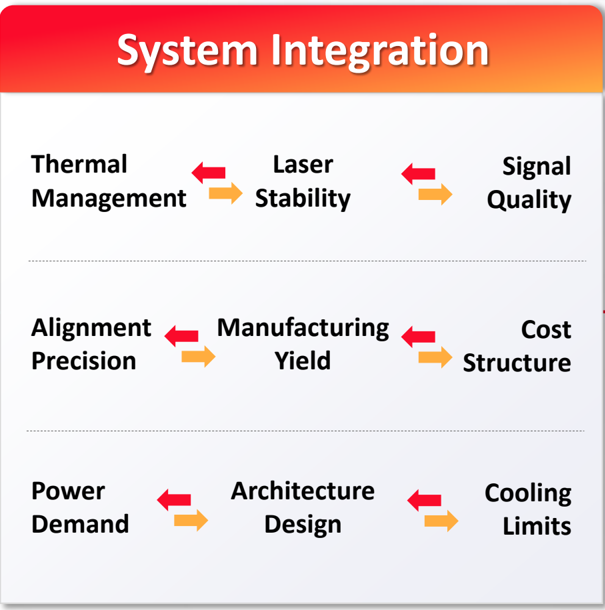
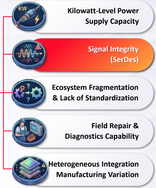
The Cost of Distance
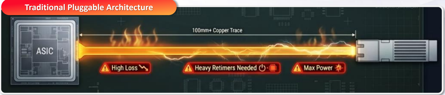
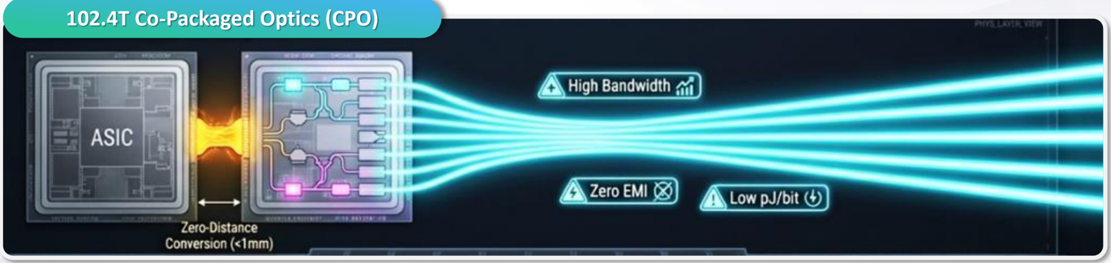
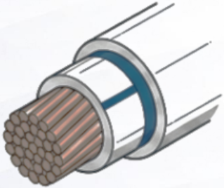
Light and electricity are not competing technologies. They are two manifestations of the exact same physical essence.
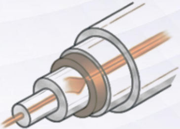
Light and Electricity : Two Quadrants of the Same Electromagnetic Field WinWay 77 It 74 $
Electrical
- Electron
- Conductor with return path
- Copper + Dielectric (Dk/Df)
- Skin effect~1dB/cm@53GHz
- mm~cm(in-package)
- Severe EMI, Coupling
Loss
~1 dB/cm v.s <0.2 dB/km
Frequency
DC~100 GHz v.s ~193 THz
Distance
mm~cm (SR) v.s cm~km (LR)
EMI
EMI Sensitive v.s EMI immune

Optical
- Photon
- Internal reflection in wave guide
- Si+SiO2
- Rayleigh scatter <0.2dB/km@1550nm
- cm~km Cross datacenter
- EMI Immune
CPO (Co-Packaged Optics)
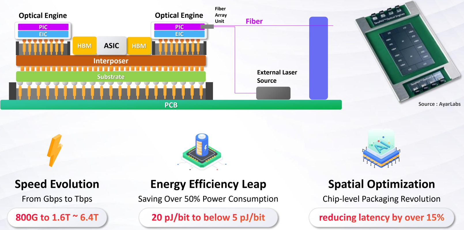
Optical Engine
Optical Circuit
~2016
Co-Packaged Optics Trend
Pluggable Optics
100% Cu
2023
OBO (On-Board Optics)
80% Cu + 20% Optics
2025
NPO (Near-Packaged Optics)
50% Cu + 50% Optics
2027
2.5D CPO (COUPE Switch)
20% Cu + 80% Optics
2030~
3D CPO (COUPE XPU)
100% Optics
| Bandwidth | ~800G | <1.6T | <3.2T | <6.4T | 12.8T~ |
|---|---|---|---|---|---|
| Power Use | 1x | ~0.8x | ~0.6x | <0.5x | <0.1x |
| Latency | 1x | <0.75x | <0.5x | <0.1x | <0.05x |
| Maintenance |
Electrical Circuit
Connector
Source : Counterpoint Research 《矽光子與共同封裝光學( CPO )報告》
Silicon Photonics Supply Chain
Source : SEMI VISION
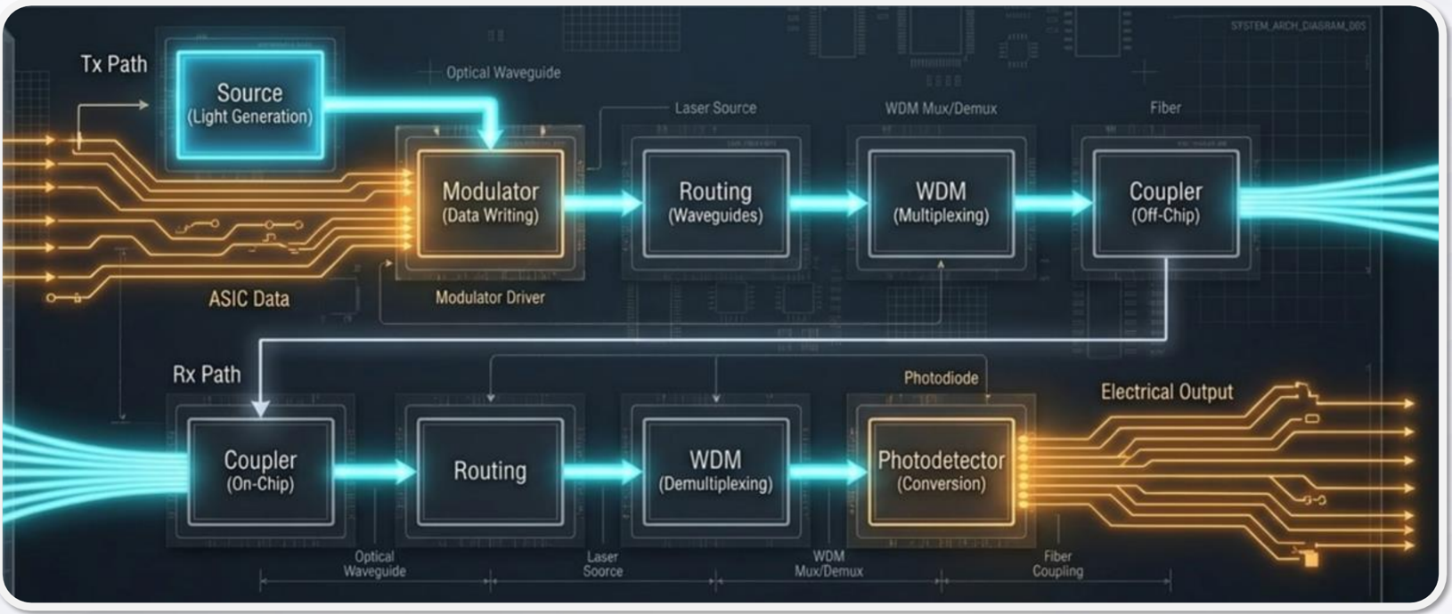
The Photonic Integrated Circuit (PIC) Blueprint
Source : Official Website
Step1 : The Light Source Matrix
DFB Laser
(Distributed Feedback)
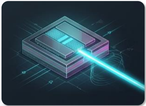
Highly Stable wavelength, narrow linewidth. Ideal for standard 1310nm/1550nm telecom.
VCSEL
(Vertical-Cavity Surface-Emitting Laser)
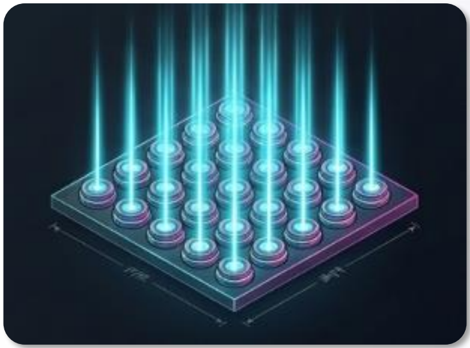
Low cost, easy to form arrays. Ideal for shortreach data centers.
Limitation : Less suited for long-reach / highpower
Comb Laser
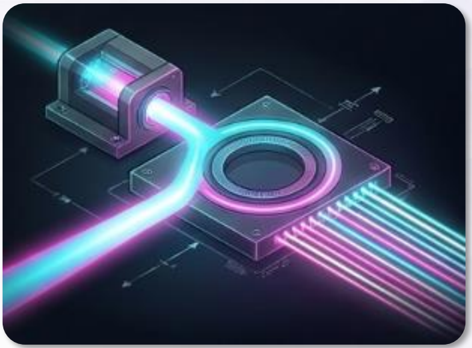
Crucial for 102.4T CPO.
Generates multiple precise wavelengths from one device, enabling massive WDM density
Step2 : The Modulator Showdown
MZM ( Mach-Zehnder )
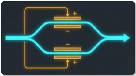
EAM ( Electro-Absorption )
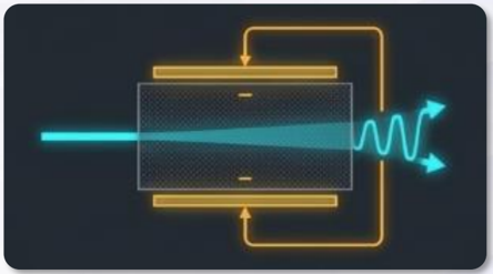
MRM ( Micro-Ring )
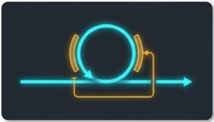
| Footprint | Large (1-3 mm) | Micro (10-20 um) | Small (50-100 um) |
|---|---|---|---|
| High | Medium | Medium | Bandwidth |
| High | Critical(Requires TEC) | Medium | Thermal Stability |
| Excellent | Moderate | Poor | PAM4 Linearity |
| Highest(10+ Yrs) | Medium | Medium | Yield / Maturity |
| Broadcom / Intel / Marvell / Lightmatter / Cisco | nVIDIA / AyarLabs | Coherent / Lumentum / Intel | Customer |
Source : Official Website
Step3 : Routing The Light
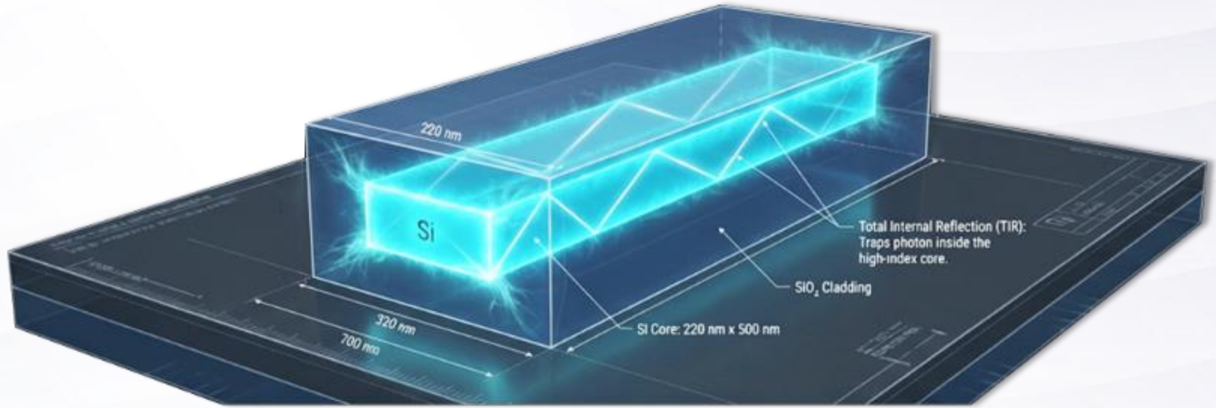

Step4 : Wavelength Division Multiplexing (WDM)
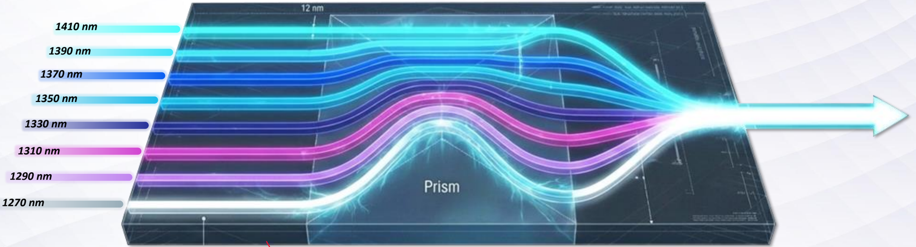
Target KPI
- Crosstalk must be maintained at -20 dB.
Step5 : I/O Coupling Strategy
Grating Couplers
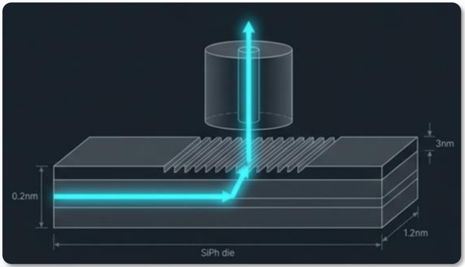
Light enters/exits vertically. High insertion loss, wavelength sensitive.
Advantage
Enables wafer-level testing (testing from the top before dicing).
Edge Couplers
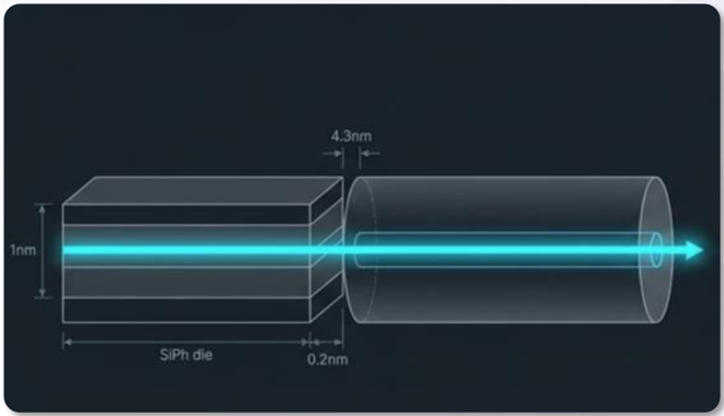
High bandwidth, ultra-low insertion loss (<1.0 dB). Polarization insensitive. Ideal for 128-core FAU.
Challenge
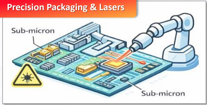
Demands extreme sub-micron alignment precision.
Different Optical Engine Design
Source : IDTechEx Research
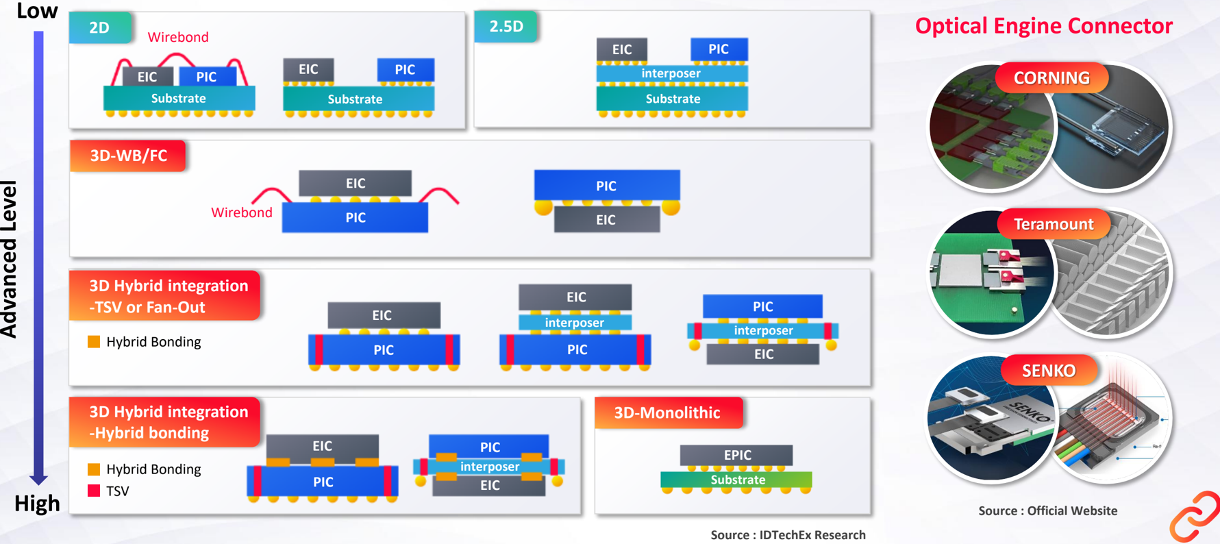
Marvell
From OE to Module / Spec Diversity
RAAHHARA
nVIDIA
nVIDIA
Lightmatter
Lightmatter
Broadcom
AyarLabs
Broadcom
Source : Official Website
Key Foundries of Silicon Photonics and CPO
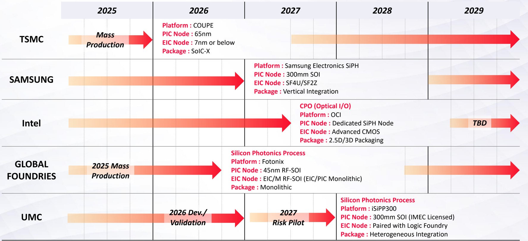
Source : DIGITIMES, 2026/04
Bottleneck of Testing in CPO Production
Winkay
Tech
CPO Test Flow / Production Bottle Neck
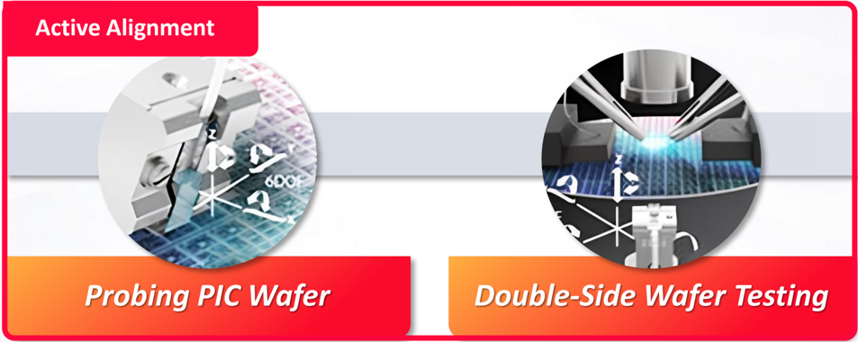
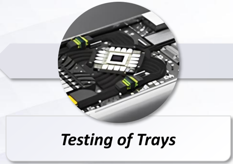
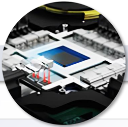
Passive Cable Attachment
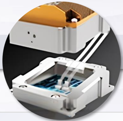
Electro-Optical Testing of Engines
Source: Teradyne
Why Must CPO Use Single Mode Fiber (SMF)?
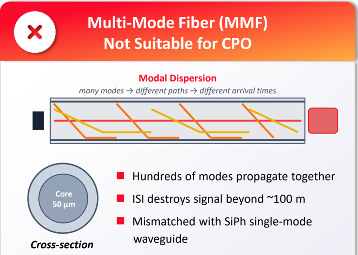
Result: collapses beyond 100 m or above 100 Gbps
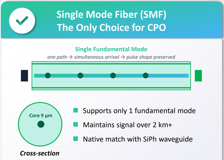
Result: enables 200 Gbps+ over 2 km+, ideal for CPO deployment
The silicon photonics waveguide itself is single-mode -light leaving the ASIC is fundamental-mode from the start. Using SMF is not a design choice for CPO; it is a physical consequence dictated at the wafer level by the silicon photonics platform.
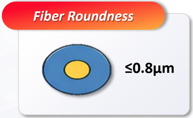
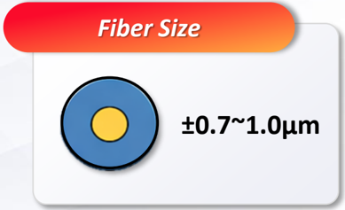
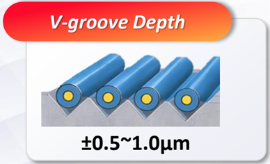
FAU Active Alignment Challenge
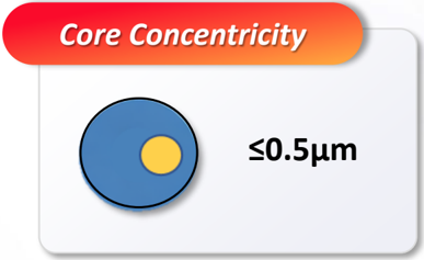
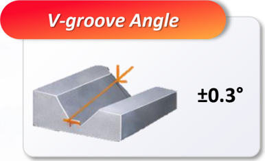
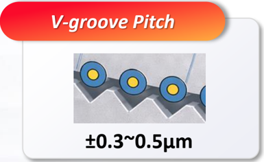
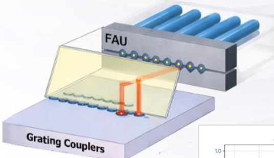
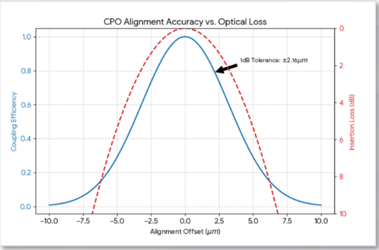
Tolerance Stack-up: 3.8 μ m| 42% of core diameter.
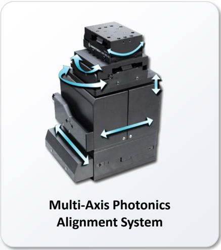
Active Alignment
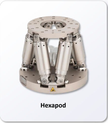
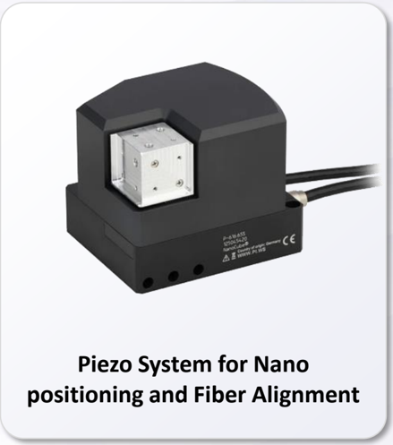

CPO Production Assessment
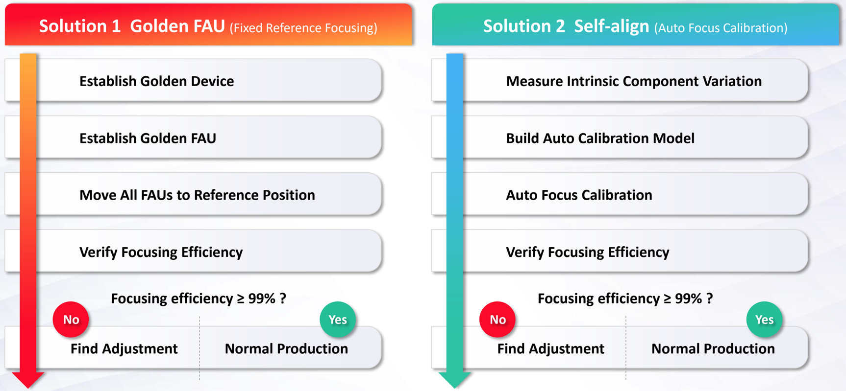
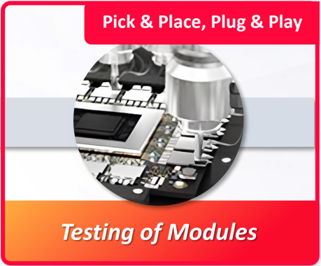
Module Test Challenge
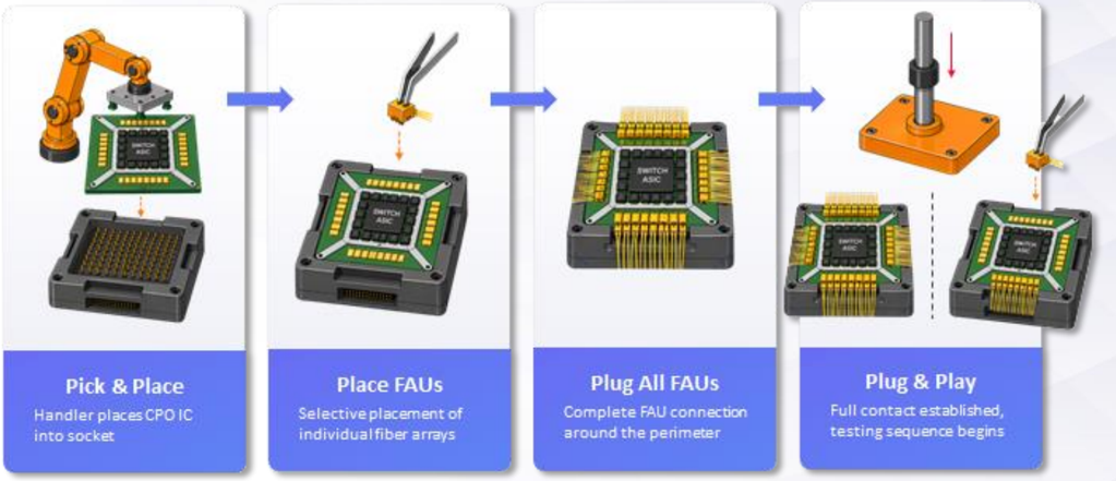
Pick & Place, Plug & Play
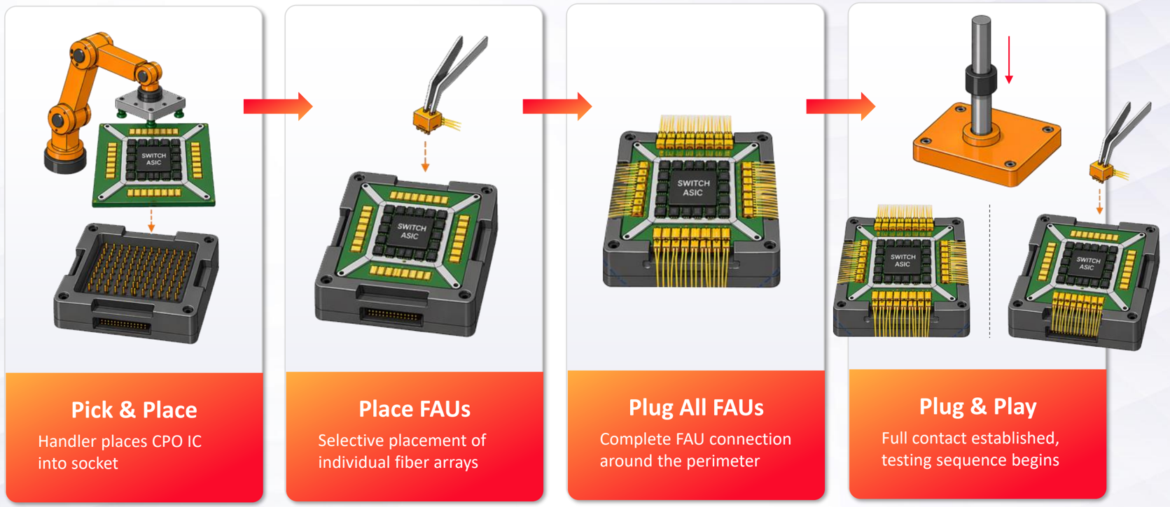
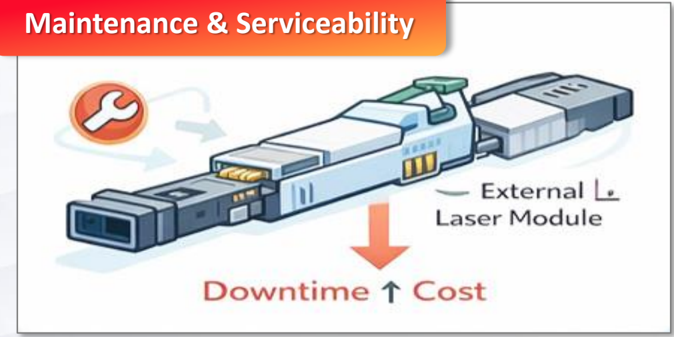
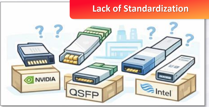
CPO Production Bottleneck Four Technical Issues

Co-Packaged Optics Test Flow
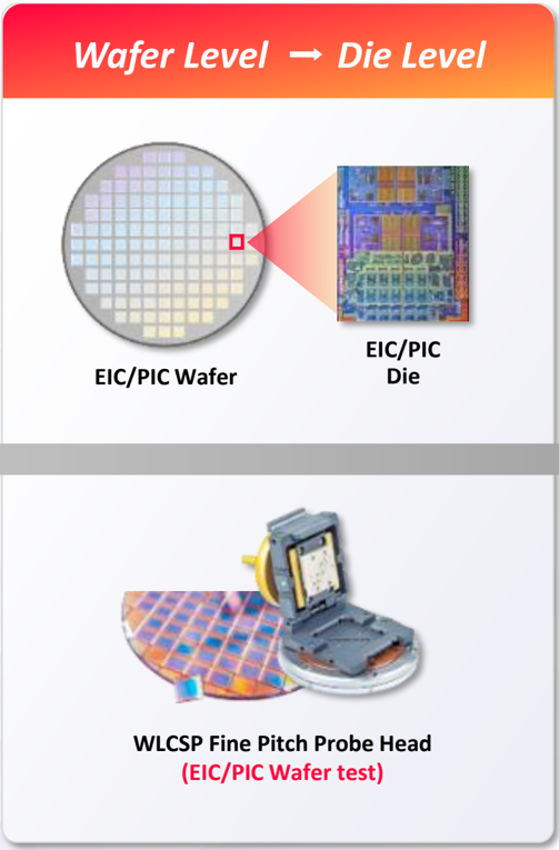
Package Level
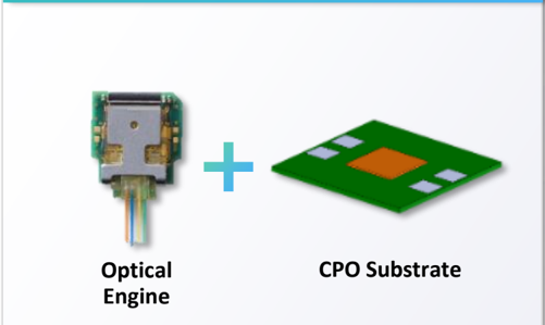
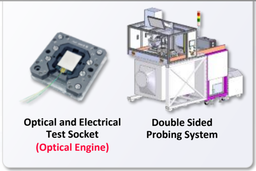
Wafer Level Test Methodology
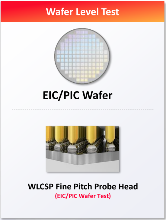
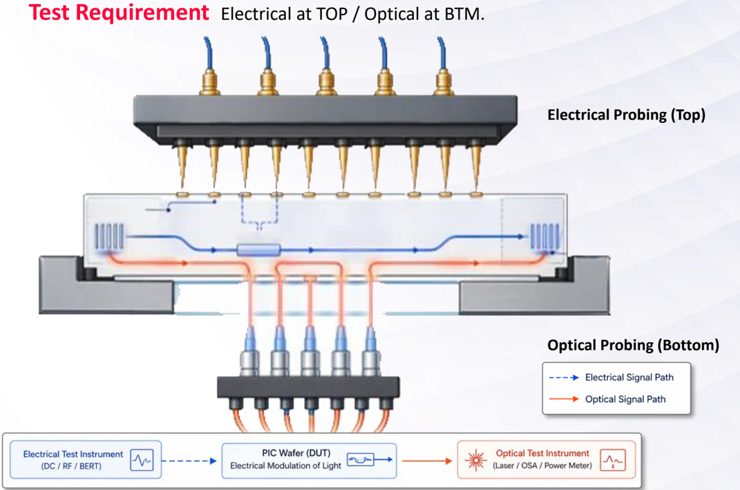
Die Level Test Methodology
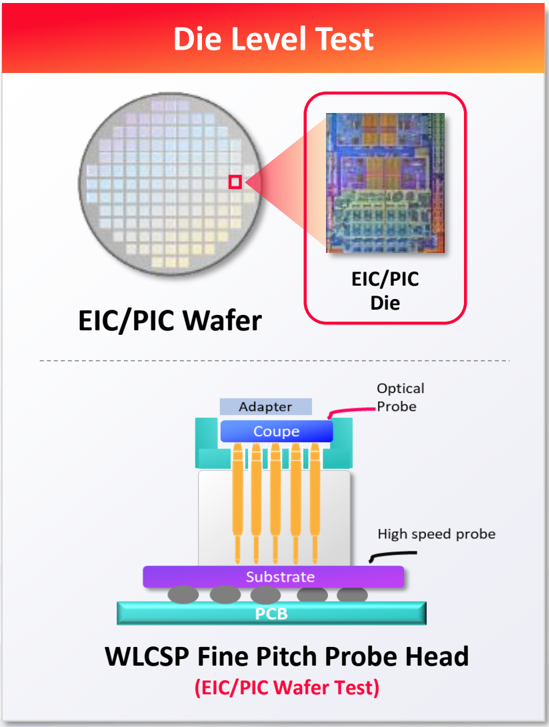
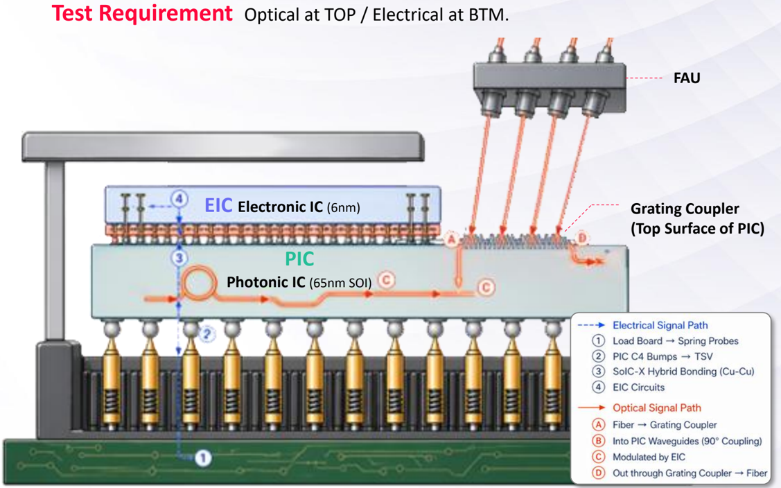
Package Level Test Methodology
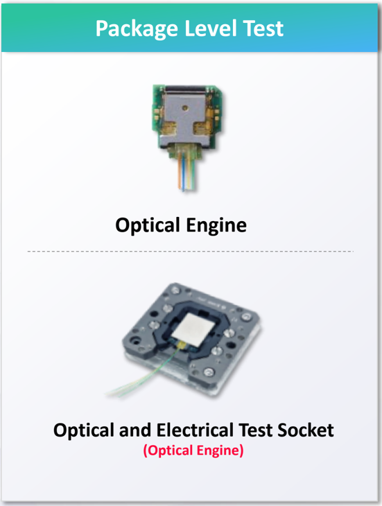
Test Requirement Active alignment , Passive alignment, Direct with FAU
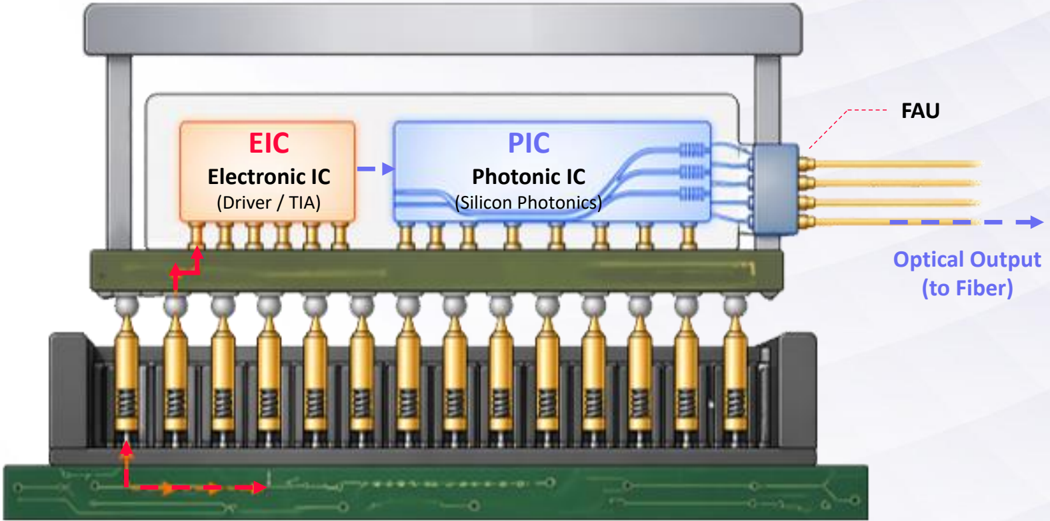
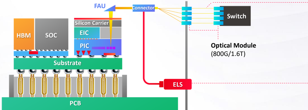
Electrical Signal Path (Load Board → EIC)
Optical Signal Path (EIC → PIC → Fiber)
Package Level Test Methodology
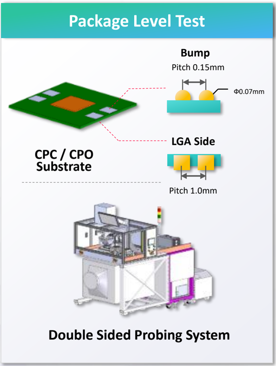
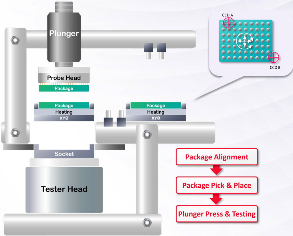
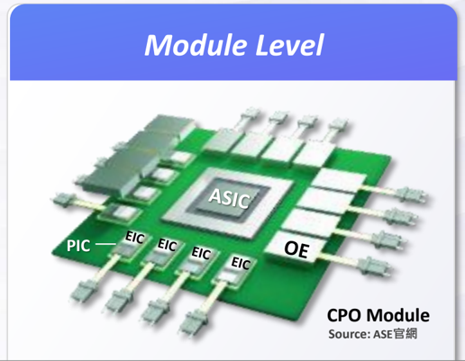
Module Level Test Methodology
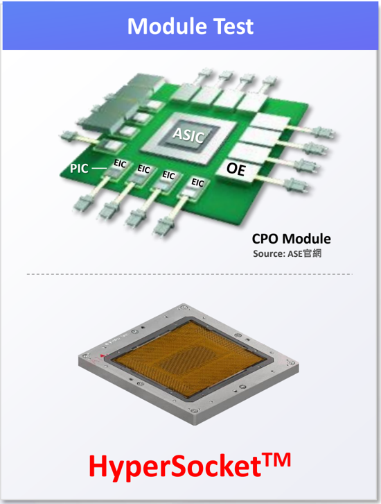
Test Requirement Test speed, Alignment, Mechanism Design.
CPO Roadmap
Winkay
Tech
COUPE : COmpact Universal Photonic Engine
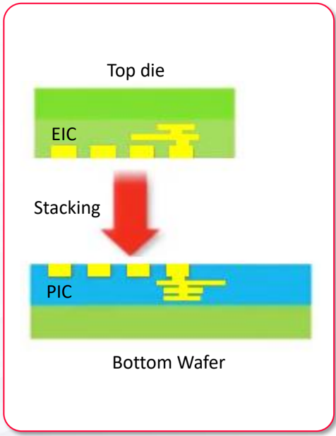
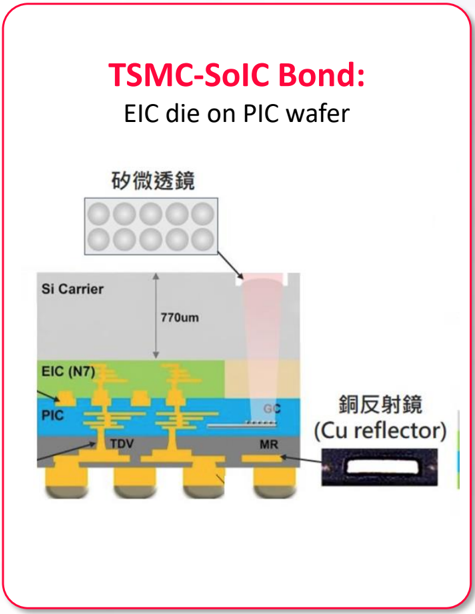
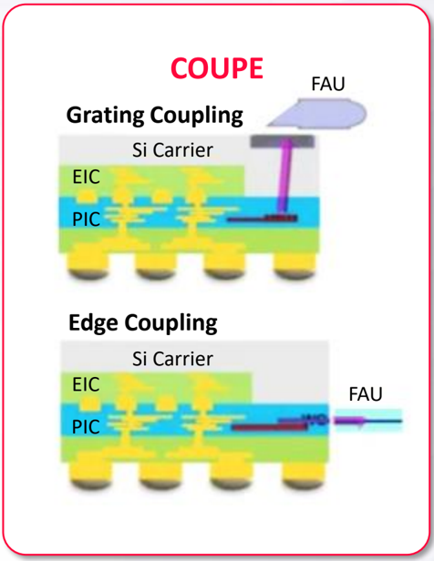
Source : TSMC
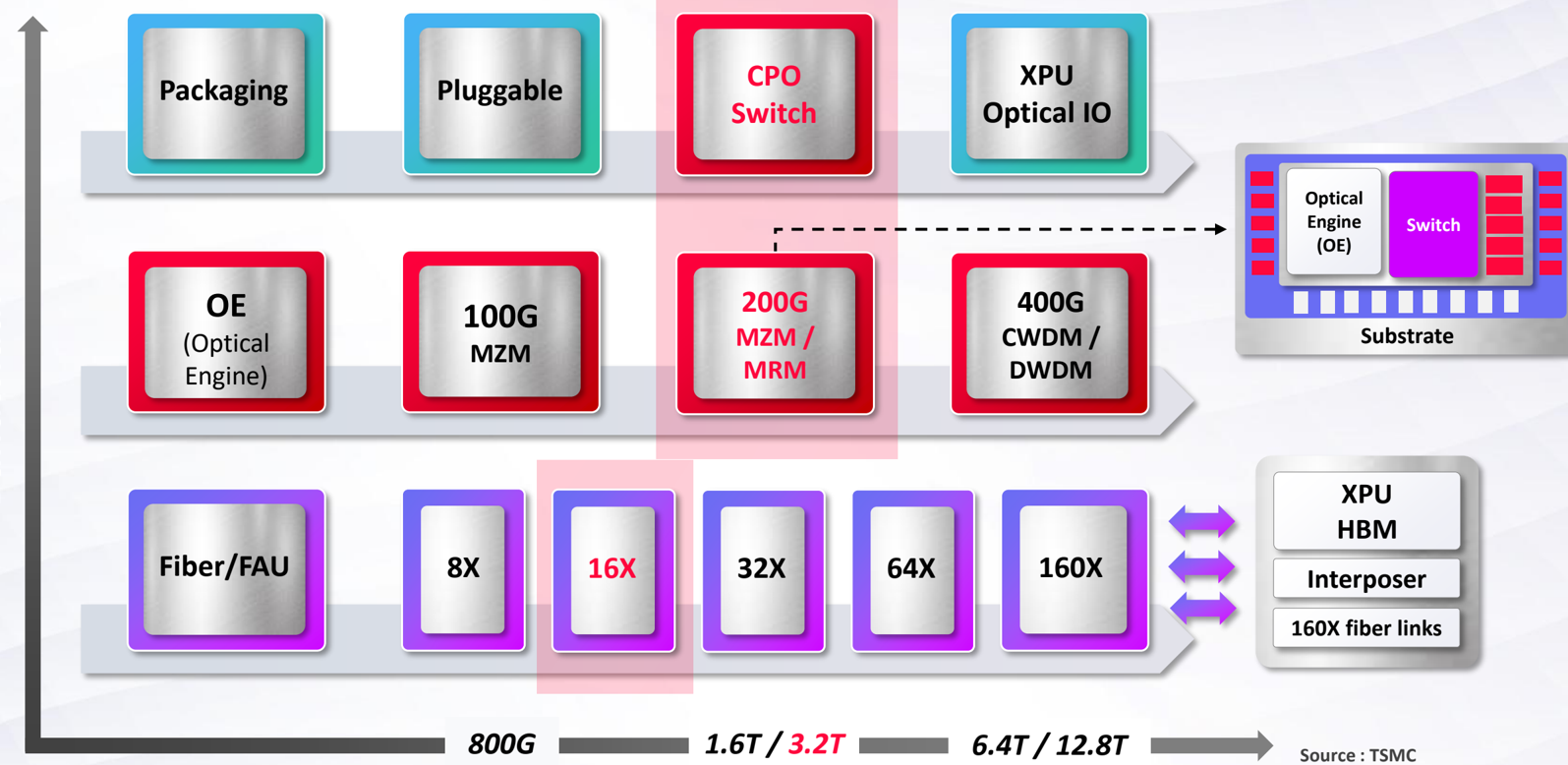
Bandwidth
CPO Roadmap
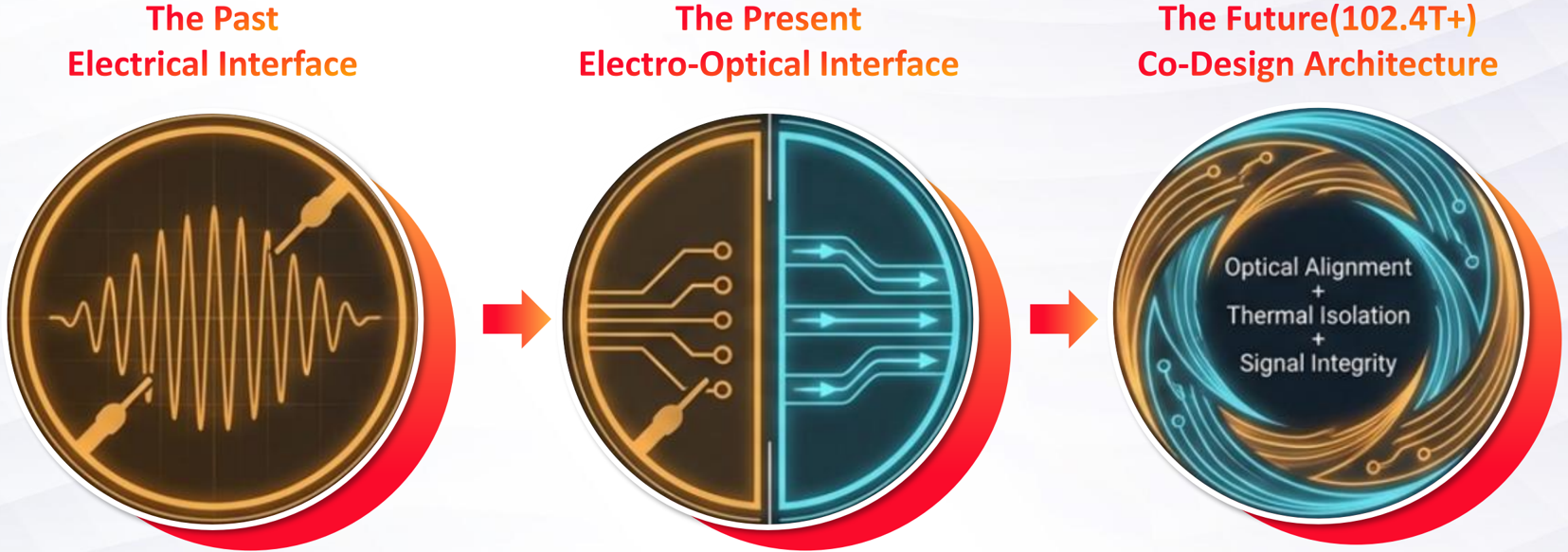
The I/O Interface Evolution
CPO/CPC Application
Winkay
Tech
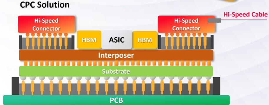
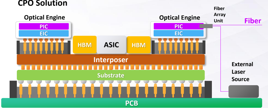
CPO / CPC Application
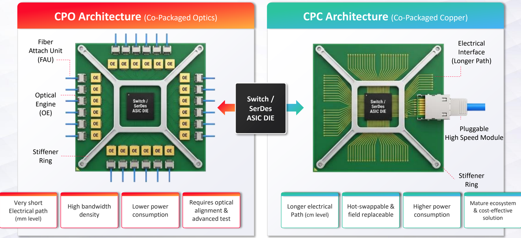
Source : Official Website
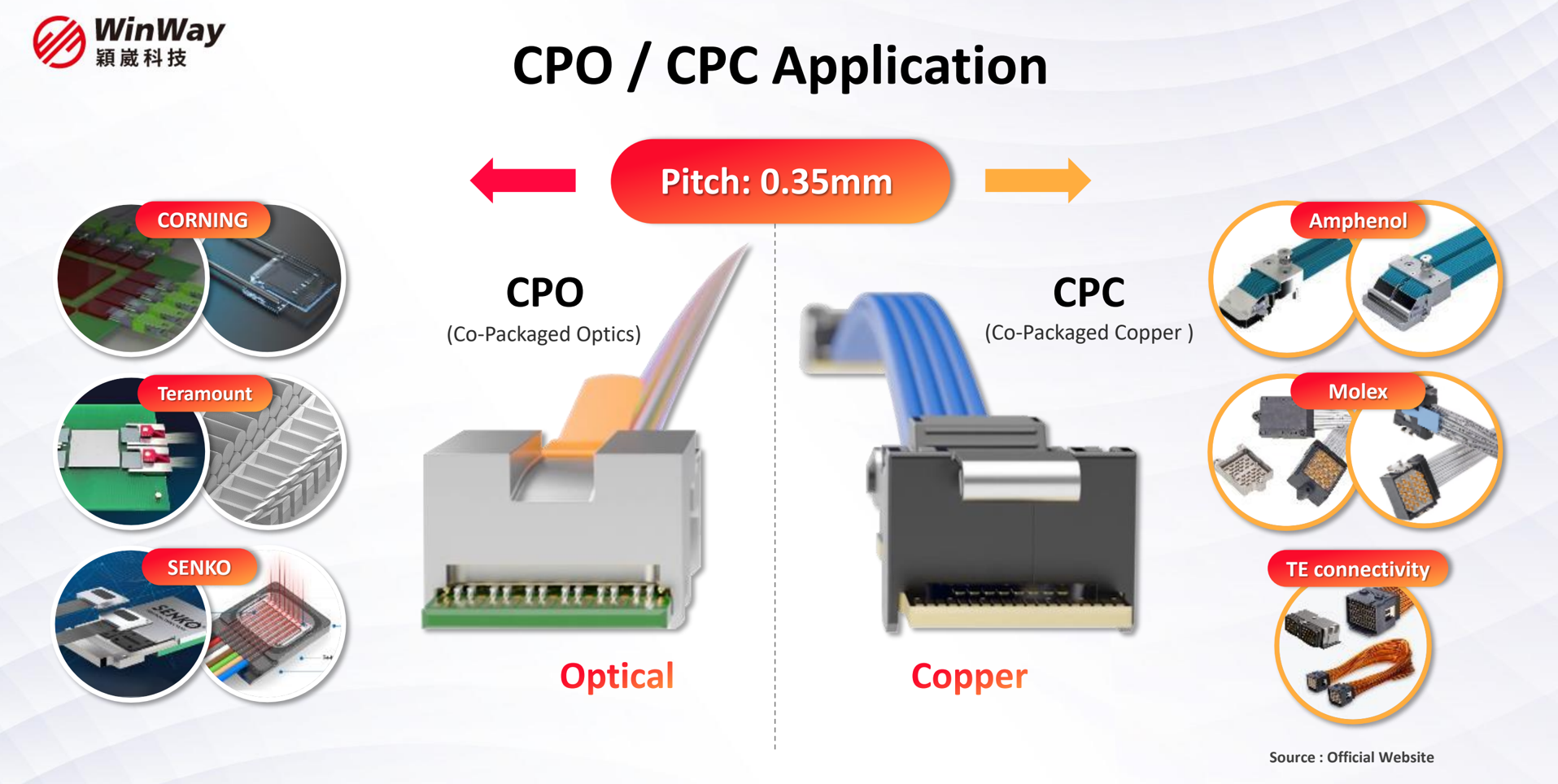
WinWay CPO/CPC Total Solution
Winkay
Tech
Future Technical Challenge
A. Mechanical Extremes
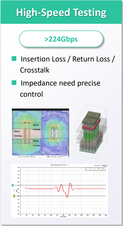
B. Electrical Performance Barriers
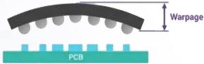
- Package Size > 100 mm up to 200mm
- Pin Count > 10,000 pins up to 50,000 pins
- Key Challenge Warpage up to 0.6mm
Technical Development Direction to 'Optics'
The challenges of package testing have evolved from a focus on mechanical machining accuracy to multi-physics coupled design , encompassing mechanical integrity, electrical performance, thermal management.
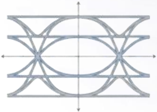
- Signal Speed 224Gbps PAM4 and beyond
- Key Challenge Signal Integrity, Crosstalk
C. Thermal Density Crisis
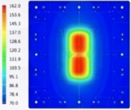
- Power Consumption > 4000W per device
- Key Challenge Thermal Runaway / Solder Melt
Interposer Size
A. Mechanical Extremes / TSMC
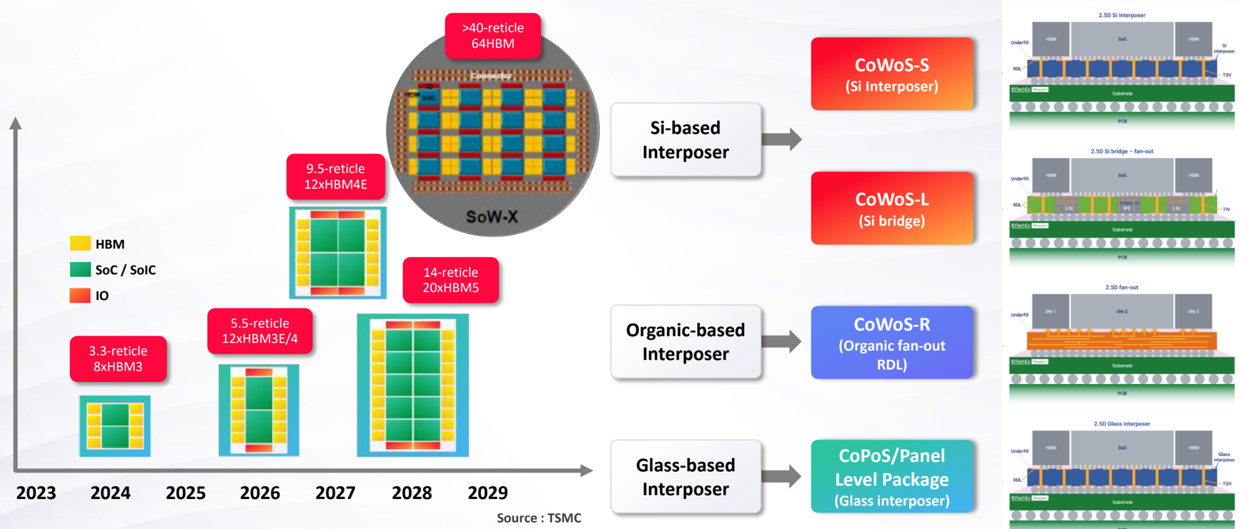
Package size dimension determine by # of Die, Memory, High Speed I/O Channel, Manufacturing limitation…
Source : IDTechEx Research
A. Mechanical Extremes /Intel
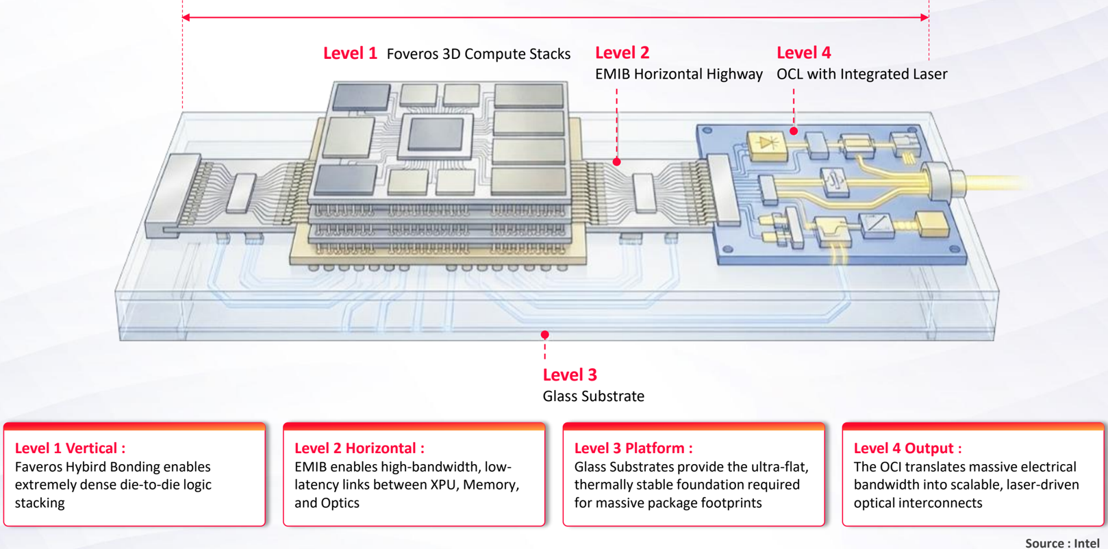
Source : Intel
B. Electrical Performance Barriers
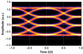
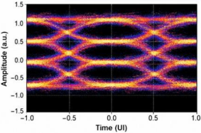
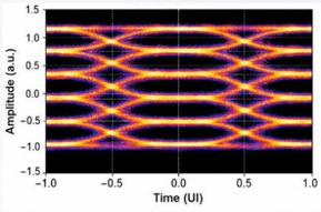
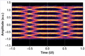
| Parameter | 224G (PAM4) | 448G(PAM4) | 448G(PAM6) | 448G(PAM8) |
|---|---|---|---|---|
| 224Gbps | 448Gbps | 448Gbps | 448Gbps | Data rate |
| log 2 4 =2 | log 2 4 =2 | log 2 6 ~2.58 | log 2 8 =3 | Bits / Symbol |
| 112 GBaud | 224 GBaud | ~173.6 GBaud | ~150 GBaud | Baud Rate |
| 56GHz | 112GHz | 86.8 GHz | 74.7GHz | Nyquist Freq. |
| 0 dB (Ref) | 0 dB (Ref) | -3.7 dB | -6.2 dB | SNR Penalty |
| Medium | High | Higher | Highest | DSP Complexity |
| Mature ecosystem : Feasible on standard PCB/Cable | Simple architecture : Best theoretical SNR. | Goldilocks Choice : Balances BW&SNR. | Low Baud Rate for 448G target | Pros |
| Requires 2X lanes to match 448G total rate. | Bandwidth Wall : Unfeasible for copper | SNR Penalty : Complex encoding logic | SNR Cliff : Requires powerful FEC | Cons |
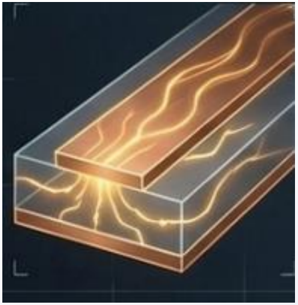
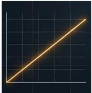
The 448G Electrical Wall
Copper Channel Loss
Insertion loss approaches -10dB on just 1 inch of premium dielectric at 112 GHz Nyquist.
Dielectric Loss Multiplier
Loss scales linearly with frequency.
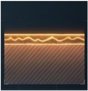
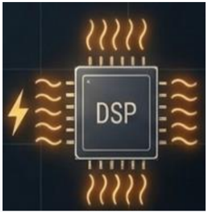
The Skin Effect Limit
At > 100GHz, skin depth drops below 0.2 um
DSP Power Explosion
Compensating for physical loss requires ADC sampling > 224 GS/s.
1 reticle Max. ~830mm 2 Chip heat density design reference : 1.1~2 W/mm 2
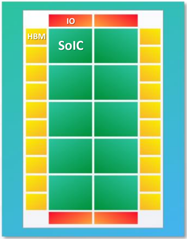
- ◼ Advanced Thermal Control System
- ◼ Higher CCC requirement (>6A/pin)
C. Thermal Density Crisis
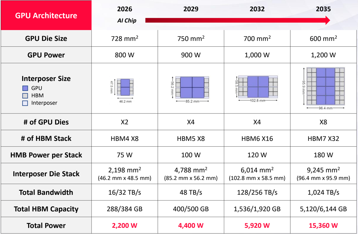
| GPU Architecture | 2026 AI Chip | 2032 | 2029 2035 |
|---|---|---|---|
| GPU Die Size 728mm | 2 750mm 2 | 700mm 2 | 600mm 2 |
| GPU Power 800W | 900W | 1,000W | 1,200W |
| Interposer Size GPU HBM Interposer | |||
| X2 | X4 | X4 | # of GPU Dies X8 |
| HBM4 X8 | HBM5 X8 | HBM6 X16 | # of HBM Stack HBM7 X32 |
| 75W | 100W | 120W | HMB Power per Stack 180W |
| 2,198mm 2 (46.2 mmx48.5 mm) | 4,788mm 2 (85.2 mmx56.2 mm) | 6,014mm 2 (102.8 mmx58.5 mm) | Interposer Die Stack 9,245mm 2 (96.4 mmx95.9 |
| 16/32 TB/s | 48 TB/s | 128/256 TB/s | Total Bandwidth 1,024 TB/s |
| Total HBM Capacity 288/384 GB | 400/500 | Source : KAIST 1,536/1,920 GB | TERALAB GB 5,120/6,144 |
| Total Power 2,200W | 4,400W | 5,920W | 15,360W |
Source : KAIST TERALAB
A+B+C : Heterogeneous Integration
CPO is the path to success in near future
The Problem with Organic Substrates
- ◼ Thermal / Mechanical Instability
- ◼ Electrical Loss
High CTE Mismatch Silicon:
Causes Warping & Misalignment
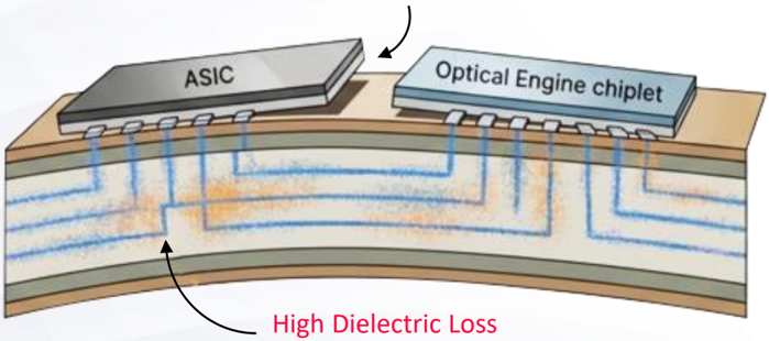
Organic Substrate
Why Glass is the Breakthrough Solution
- ◼ Superior Stability
- ◼ Pristine Electrical Performance
- ◼ Advanced Integration
Near-Perfect CTE Match to Silicon:
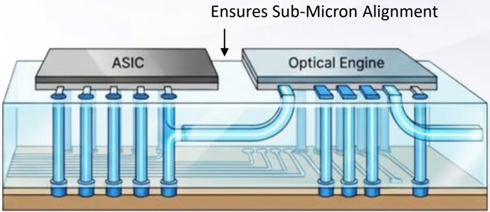
Glass interposer / Substrate
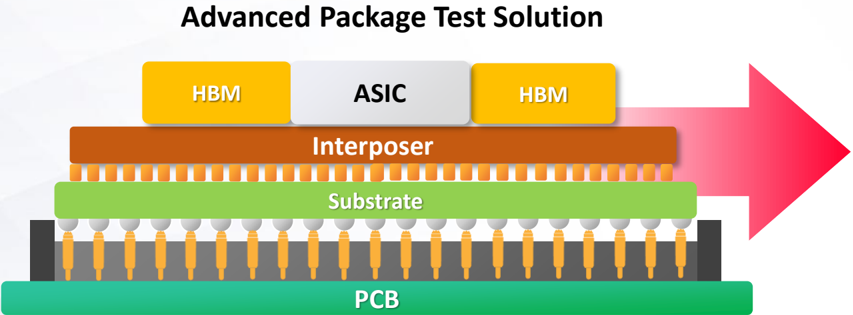
Challenges of Advanced Package Test Solutions
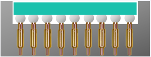
High Pin Count
>20KPin
- ◼ Preload force
- ◼ Maintenance
- ◼ Random fail concern
Housing Warpage by Preload
Contact Resistance random fail (If 20 pin fail/20,000~0.1%)
High Heat Density
>4000W
- ◼ Socket thermal domain
- ◼ Thermal run away
IC>4000W
Socket Power Loss>500W
Socket housing thermal distribution
Innovation of Hybrid Architecture / Conventional Test Interface
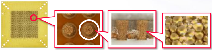
Elastomer
Spring probe
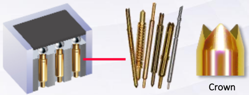
| Length(mm) | 0.5~2.0 | ★ 1.5~6 even longer depend on the requirement |
|---|---|---|
| ★ <50 (Multiple contacts) | <60 (Design dependent, including probe structure) | Resistance (mohm) |
| 0.2(Min.)~0.4(Max.) | ★ 0.35(Min.)~1.0(Max.) | Travel (mm) |
| 20~50/per bump | ★ 15~25/per pin | Force(g) |
| ~4 | ★ Up to 6 | CCC(A) |
| Not really applicable | ★ Applicable | Coaxial Structure |
| ★ clean by sticker | clean by brush/clean pad/laser | Maintenance |
| Whole piece, but easy to replace | ★ Individual probe replaeable, but take times to replace &maintenance | Spare part |
| • Hard to balance lower force <20g, contact resistance and lifetime PS: Normally, reflected force varies from 30~50g/per bump • Shorter contact travel <0.4mm(Max) to cover package warpage • Shorter lifetime (can not replace individually) • No coaxial structure for large package application | • Limited four contact points of top plunger design • Need regular clean to maintain Cres • Physical damage to solder ball and pad if wrong setup | Limitation |
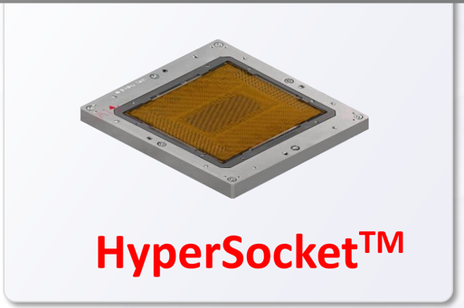
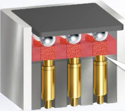
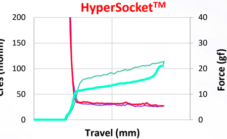
Innovation of Hybrid Architecture HyperSocket TM
Contact Resistance
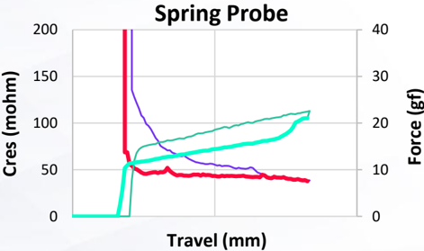
Cres (mohm)
Current Carrying Capacity
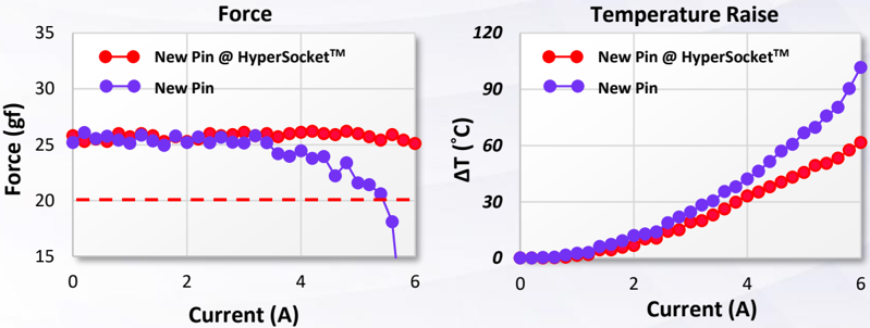
Why HyperSocket is suitable for Advantaged Package Testing(Ultra Large Package)?
| Limitation | Characteristics |
|---|---|
| Elastomer Lifetime | Significantly increase contact surface between contactor to solder ball and PCB pad |
| Higher Initial investment | Less and stable contact resistance↓30% |
| Higher current carrying capacity(C.C.C.)↑30% Less joule heat generation by high current↓30% No housing warpage of spring probe socket Lower total test cost of ownership: Factory operation, | |
| Hardware, Maintenance and Test interface including Change Over Kit, Socket, PCB. |
Innovative Test Solution HyperSocket TM
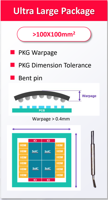
Requirements for HyperSocket TM Design
-
◼ Package Size
-
◼ Pin count
-
◼ Device Warpage
-
◼ High Current Density
-
◼ SACQ(Frequent Clean)
-
◼ Solder Ball Melting
-
◼ Probe bent and worn out issue
>100 X 100 mm 2
>10,000 pin
>0.4 mm
>6 A
~10 TD
Patent NO .
- TWI862047
- TWI922268
- TWI862191
- TWI901161
- TWI884802
- TWI923382
Hyper-UF
Frequent Clean, Solder Ball Melting
Hyper-DH
High Current Density, Probe Bent
Hyper-LF
Ultra Large Package, High Pin Count
Hyper-Liquid
Under Validation
Extremely High Power > 2500W
- TWI901181
- CN220584352
- US(Granted )
Summary
Winkay
Tech
CPO Market Trends & Challenges

2026 - 2028 is the golden window for ASIC platform flexibility.
One ASIC supporting both CPO and CPC -Scale-up via CPO for performance, Scale-out via pluggable for flexibility.
NVIDIA SIGNALS
- 1.6T CPO saves 180MW at million-GPU scale
- Spectrum-X: 5 × efficiency, 2Tb/s, 10 × reliability
- CPO and copper coexist, layered deployment
FUTURE TRENDS
- Scale-up is the main battlefield
- Adoption: coexist → expand → mainstream
- ELS architecture, DSP-free design
CORE CHALLENGES
- Thermal & yield: one defect kills package
- Serviceability: operations SOP rebuilt
- Standards & cost: ecosystem immature
WinWay is Ready for CPO & CPC Testing
Q
Your Trusted Partner in Semiconductor Testing
THANK YOU
You may contact WinWay Technology via sales@winwayglobal.com
+886 7 361 0999 / +886 3 656 8282
www.winwayglobal.com