PDF 原檔:報告_IEEE_EPS_JohnLau玻璃封裝與可靠度_20260924_original.pdf
圖片清單(已驗證 2026-09-29)
ingest 時建立的「眼見為憑」圖片索引;<40KB 未逐張 Read(預設 logo,免列)。80 頁投影片前段(001-017)多為 IEEE EPS 學會簡介與素材庫照片,非玻璃封裝技術內容;技術圖解集中在 018 之後。
| 檔名 | size | 分類 | 親眼所見內容 |
|---|---|---|---|
_001.png |
145KB | 裝飾·素材庫照片 | 風力發電機+太陽能板天空背景圖 |
_002.png |
170KB | 裝飾·素材庫照片 | 電路板特寫(電容、IC 晶片) |
_003.png |
136KB | 裝飾·素材庫照片 | 全息投影技術感的女性研究員 |
_004.png |
137KB | 裝飾·素材庫照片 | 亞裔男學生手持電路裝置 |
_005.png |
157KB | 裝飾·素材庫照片 | 機械手指觸碰電路板特寫 |
_006.png |
289KB | 文字卡 | IEEE EPS(Electronic Packaging Society)組織介紹輪盤圖:Awards/Membership/Technical Committees/Conferences/Publications/Education 六區塊 |
_007.png |
131KB | 裝飾·banner | IEEE EPS Certificate Program 宣傳 banner |
_008.png |
132KB | 文字卡 | EPS Resource Center 六張論文/簡報封面縮圖拼貼 |
_009.png |
107KB | 裝飾·會議照片 | 三人於戶外餐會合影(會議社交場合) |
_010.png |
99KB | 裝飾·會議照片 | 會場觀眾席照片 |
_011.png |
46KB | 裝飾·會議照片 | 講者站於 ECTC 講台照片 |
_015.png |
50KB | 裝飾·logo | 「DTMES」綠色標誌 |
_017.png |
42KB | 文字卡 | IEEE EPS 全球分會地圖(世界地圖+分會數統計,非玻璃封裝技術內容) |
_018.png |
90KB | 真資料圖 | CPO with Glass Photonics 架構圖:ASIC Switch + Laser Driver/InP Laser/TIA/Germanium PD 經 Cu 連接玻璃波導/耦合器至光纖,標示 Glass Bench、TSV/Cu-Cu |
_019.png |
250KB | 真資料圖 | FOPLP 玻璃暫時載板製程 (a)-(d):Carrier 1 bonding → KGD die bonding → Dry film lamination → Carrier 2 bonding & Carrier 1 de-bonding |
_020.png |
173KB | 真資料圖 | FOPLP 製程 (e)-(g):RDL → 錫球植球 → 半導體後段;右側 9mm×9mm 完成品實照,紅字標註「FOPLP with RDLs substrate/There is no glass substrate」 |
_021.png |
251KB | 真資料圖 | KGD 完整製程:device wafer 測試 → 玻璃暫時載板(LTHC 犧牲層)→ die face-up → compression molding EMC → 磨薄 → RDL/植球 → 雷射解鍵合切割 (a)-(h) |
_022.png |
127KB | 真資料圖 | 300mm 晶圓 → 13.4mm×13.4mm 單元 → 10mm×10mm 晶片尺寸示意 |
_023.png |
132KB | 真資料圖 | Organic-core substrate vs Glass-core substrate 2D 結構剖面對比圖:CHIP/HBM/CHIPLET + C4/µbump + ABF/PID RDL + PTH(有機)/TGV(玻璃)+ solder ball + PCB |
_024.png |
126KB | 真資料圖 | Woven Glass Laminate Core 剖面圖:Die-RDL-PTH-玻纖布層-RDL-solder ball |
_025.png |
146KB | 真資料圖 | Glass Core + TGV + RDL 剖面圖(與上圖對照的玻璃芯版本) |
_026.png |
302KB | 真資料圖 | Silicon TSV-interposer vs Glass TGV-interposer 完整結構對比圖:SoC/HBM 經 µbump 接 interposer(矽 TSV 或玻璃 TGV)→ ABF RDL → organic-core substrate → solder ball → PCB;右側分別標示「2.5D (CoWoS)」與「2.5D (CoPoS)」 |
_027.png |
251KB | 真資料圖 | TSV-interposer 完整結構圖(含晶片實照插圖),標示 RDL L/S=0.2µm min,下方紅字「CoWoS has been in HVM since 2013.」(原簡報第 20 頁) |
_028.png |
228KB | 真資料圖 | 同上但為 TGV-interposer 版本,右側標示「Glass Panel Size: 310mm x 310mm」 |
_029.png |
258KB | 真資料圖 | CoWoS-L with Embedded LSIs (Si-Bridges) 結構圖 (a) 簡化版 (b) 詳細版:RI(Reconstituted-Interposer)= Si Bridge 埋入 Fan-Out EMC |
_030.png |
330KB | 真資料圖 | 玻璃版 Reconstituted-Interposer 結構圖:Si Bridge Wafer + Glass Temporary Carrier Wafer → Glass-core package substrate,標示 Glass Panel 310mm×310mm |
_031.png |
412KB | 真資料圖 | Unimicron 美國專利 11,410,933(2021-05-07 申請)剖面圖:Si Bridge RDL by 64nm process technology(L/S=0.2µm min),Chip 1/Chip 2 經 C2/C4 bump 接 Si Bridge,EMC+TMV+Package Substrate |
_032.png |
396KB | 真資料圖 | 「CoWoS」黃底標題版簡化結構圖(TSV-interposer + organic substrate) |
_033.png |
537KB | 真資料圖 | 「CoPoS-v1」黃底標題版結構圖(TGV-interposer + organic substrate,玻璃 panel 310×310mm) |
_034.png |
585KB | 真資料圖 | 「CoPoS-v2」黃底標題版結構圖(TGV-interposer + glass-core substrate) |
_035.png |
76KB | 真資料圖 | CoPoS-v3:Bridge Embedded in Panel Fan-Out EMC with RDLs 結構圖 |
_036.png |
144KB | 真資料圖 | CoPoS-v3 續(RI/EMC 結構 + Glass Temporary Carrier + Glass Panel 310×310mm 標註,原簡報第 30 頁) |
_037.png |
141KB | 真資料圖 | WLP vs PLP 面積效率對比圖:300mm 晶圓 8 顆 substrate/interposer(效率~50%)vs 310×310mm 面板 16 顆(效率~88%) |
_038.png |
597KB | 真資料圖 | TSV 傳統製程步驟圖(Si substrate→SiO2→photoresist→DRIE→PVD barrier+seed→Cu plating→CMP)+ SEM 剖面照(100µm TSV,頸縮 0.40/0.44/0.83µm,底徑 8.67µm) |
_039.png |
537KB | 真資料圖 | PECVD+Dual Cu-Damascene+CMP RDL 製程圖 + SEM 剖面照(UBM/RDL3/RDL2/RDL1/TSV 尺寸標註),黃字「RDLs minimum pitch = 0.4µm」 |
_040.png |
584KB | 真資料圖 | (a) TGV Process flow (b) SEM image of TGV (c) 蝕刻機制示意(OH/F 離子攻擊玻璃孔壁) |
_041.png |
80KB | 真資料圖 | TGV 金屬化示意:(a) 側壁鍍膜前 (b) 電鍍填銅後,Glass/TGV/Cu 標註 |
_042.png |
82KB | 真資料圖 | SEM 剖面照放大:Cu/TGV/Glass 三色區塊特寫 |
_043.png |
181KB | 真資料圖 | TGV+RDL 完整製程對照:(a) PID/ABF 聚合物增層路線 (b) PECVD SiO2+Dual Cu-damascene 路線,皆以 Glass Core Panel 為基材 |
_044.png |
95KB | 真資料圖 | SEM 剖面照:Build-up layers (RDLs) / Glass core (內含多支 TGV) / Build-up layers (RDLs) 三層結構全視野 |
_045.png |
187KB | 真資料圖 | SEM 剖面照放大:Cu-filled TGV/Cu-pad/Dielectric/Build-up layers 標註(原簡報第 40 頁) |
_046.png |
45KB | 真資料圖 | 600mm×600mm panel 可容納 4 顆 300mm wafer 示意圖 |
_047.png |
39KB(<40KB,仍逐張確認) | 真資料圖 | 與 037 相同主題的簡化重複版:300mm 圓(8 Interposers,效率~50%)vs 310×310mm 面板(16 Interposers,效率~88%) |
_048.png |
705KB | 真資料圖 | ASE 官方簡報頁(右上角 ASE logo):300mm Wafer vs 310×310mm Panel 屬性比較表(Shape/Edge Waste/Area Utilization <60% vs >85%/Capacity/Material Utilization/Equipment Throughput,皆為 Higher),註:Die per panel vs wafer 通常 >1.5x(3.5x reticle size 下) |
_049.png |
151KB | 真資料圖 | CTE 失配結構圖:Organic Core(αx=αy=11.3、αz=24.8 ×10⁻⁶/°C)vs Glass Core(α=6.3×10⁻⁶/°C)與 PCB(αx=αy=18、αz=70)對比 |
_050.png |
201KB | 真資料圖 | corner µbump 累積等效非彈性應變曲線圖:Glass core substrate 4.43%/cycle vs Organic core substrate 9.12%/cycle(皆有 underfill 保護) |
_051.png |
207KB | 真資料圖 | C4 corner solder joint 累積等效非彈性應變曲線圖:Glass core substrate 19%/cycle vs Organic core substrate 8.43%/cycle(PCB 側無 underfill 保護) |
_052.png |
76KB | 真資料圖 | BGA solder joint 對稱模型示意圖(Chip/Equivalent block/PCB,無 underfill) |
_053.png |
180KB | 真資料圖 | CTE 失配結構圖重複版+µbump(Sn0.7Cu)/C4(SAC305) 材料標註,紅字結論「Strain and stress are larger!」(玻璃版) |
_054.png |
113KB | 真資料圖 | Glass-core build-up substrate 尺寸標註圖:20mm×20mm 晶片、800µm 玻璃核心、Cu trace/SiO2 各 1.5µm、40mm×40mm PCB(not-to-scale) |
_055.png |
198KB | 真資料圖 | Poisson's ratio 等效模型簡化圖(815µm 實際結構 → 813.5µm equivalent block) |
_056.png |
122KB | 真資料圖 | Cu 材料應力應變曲線圖:Yield Stress=173MPa、E=121GPa、Tangent Modulus=1.2GPa |
_057.png |
598KB | 真資料圖 | Cu-Cu hybrid bonding FEM 網格模型:1/4 model + Solder Joint/Cu Pad 細/粗網格對比 |
_058.png |
136KB | 真資料圖 | 熱循環邊界條件圖:5 個循環,85°C 至 -40°C 溫度曲線 |
_059.png |
67KB | 真資料圖 | 85°C 側視形變等高線圖(色階 0 至 84.353µm) |
_060.png |
71KB | 真資料圖 | -40°C 側視形變等高線圖(色階 0 至 -119.45µm) |
_061.png |
43KB | 真資料圖 | 四分之一模型應力等高線圖(局部放大,紅橙為高應力角) |
_062.png |
42KB | 真資料圖 | 同上另一時間點應力等高線圖(色階分布不同) |
_063.png |
64KB | 真資料圖 | 結構形變時間歷程圖:5 個循環間震盪於 +75µm 至 -115µm |
_064.png |
86KB | 真資料圖 | Corner Cu pad 應變等高線圖(450s,數值趨近 0) |
_065.png |
148KB | 真資料圖 | Corner Cu pad 應變等高線圖(2250s,最大 4.7×10⁻⁶) |
_066.png |
152KB | 真資料圖 | Corner Cu pad 應變等高線圖(18000s,最大 1.3×10⁻⁵,紅色熱點浮現) |
_067.png |
873KB | 真資料圖 | Cu-Cu hybrid bonding FEM 網格 + 85°C/-40°C 應力等高線大圖(Max Stress 163-180MPa,位於 Chip-Cu pad 界面) |
_068.png |
844KB | 真資料圖 | Solder Joint FEM 網格 + 85°C/-40°C 應變等高線大圖(0.043 至 0.13 max,Glass-core substrate 與 solder 界面) |
_069.png |
139KB | 真資料圖 | Corner solder bump 累積等效非彈性應變曲線圖:16.02%/cycle(單一情境) |
_070.png |
62KB | 真資料圖 | 形變曲線對比:Glass CTE=4.8×10⁻⁶/°C(紅,形變較大)vs CTE=10×10⁻⁶/°C(藍,形變較小) |
_071.png |
174KB | 真資料圖 | Corner Solder Joint 應變曲線對比:Glass CTE=4.8×10⁻⁶/°C(16%/cycle)vs CTE=10×10⁻⁶/°C(8%/cycle) |
_072.png |
287KB | 真資料圖 | CPO 玻璃基板/中介層異質整合專利圖(TW Patent I936450,2024-04-12 申請):Switch/EIC/PIC 經 Cu-Cu hybrid bonding 與玻璃波導/光纖耦合器整合 |
_073.png |
117KB | 真資料圖 | 3.5D 異質整合結構圖:SoC/HBM/ASIC Switch/OE 陣列於 TGV-interposer 上之 Top-View 與 X-View(TGV-interposer L/S=0.2µm min) |
_018、_072、_073涉及 CPO(Co-Packaged Optics)玻璃波導/中介層整合,屬本份講座的旁支主題;本批次依批次規則不改寫既有 技術_CPO 頁,故這三張圖暫不嵌入任何 lib 頁,僅列此清單存查。
原始內容
Glass Packaging and Its Reliability
(IEEE Santa Clara Valley EPS Chapter Distinguished Lecture)
John H Lau Unimicron Technology Corporation John_Lau@unimicron.com September 24, 2026
This Lecture is supported by the IEEE Electronics Packaging Society's Distinguished Lecturer Program
eps.ieee.org
2
IEEE Electronics Packaging Society (EPS)
'Emerging technologies-such as AI, 5G, edge, cloud, and data center, autonomous vehicles and wearable technology hold great promise for improving the lives of individuals across the globe,'(HIR)
Highlights of the EPS Education Programs
EPS Certificate Program
- EPS Achievement Certificate
- EPS Distinguished Achievement Certificate for Technical Leadership and Expertise
- EPS Distinguished Achievement Certificate for Professional Engagement and Service
EPS Distinguished Lecturer (DL)
- 34 DL's covering a multitude of topics
- Talks at Chapters/Universities & Conferences
Resource Center (Resource Center IEEE EPS)
- Heterogeneous Integration Roadmap: Presentations, 24 Technology Specific Chapters
- Featured Papers/ Reports
- EPS Newsletters
- > 100 Technical Webinars
- Education Materials
(EPS VP, Education -Eric Perfecto)
25+ Conferences / Workshops + CPMT Transactions
North America
ECTC
Asia
Europe
EPS Flagship Conferences
40+ Chapters Around the World
6
- ➢Introduction
- ➢Definition of Glass Packaging
- ➢Glass as a Temporary Wafer or Panel Carrier
- ➢Intel's Glass-core Substrate
- ➢TSMC's Glass-core Substrate/Interposer
- ➢Panel Size Update
- ➢Solder Joint Reliability on Glass-core Substrate
- ➢Summary and Recommendations
CONTENTS
In the past
The performance of a semiconductor product has been driven by Moore's Law. Today, 2nm is in high volume manufacturing.
Now and the future
The performance is not only driven by purely Moore's Law but also by:
- how the chips are partitioned and split into smaller chiplets
- how the chiplets are stacked
- how the chiplets are interconnected (Bridges)
- how the chiplets are cooled
- how the chiplets are packaged
The methods, among others, are:
- Chiplets heterogeneous integration [1, 2, 3, 4, 5, 7]
- Bridges connecting chiplets [1, 2, 3, 4]
- FOWLP/FOPLP, TCB, Cu-Cu hybrid bonding [1, 2, 3, 4, 5, 8]
- Panel-level packaging [1, 8]
- Glass packaging [1. 2]
- Co-packaged optics with Si/Glass photonics [1, 2]
- Superior quality and reliability [1, 2, 3, 6]
- Superior thermal management [2]
- Innovative materials and processes [1 - 10]
- Integrate into the existing manufacturing environments
- etc.
- [1] Lau, J. H., and K. N. Chiang, Hybrid Bonding, Glass, and Al-Assisted Simulation for Chiplets Heterogeneous Integration, (547 pages), Springer, 2026.
- [3]Lau, J. H., Flip Chip, Hybrid Bonding, Fan-In, and Fan-Out Technology, (501 pages), Springer, 2024.
- [2] Lau, J. H., and X. Fan, Hybrid Bonging and Thermal Management for Chiplets and Heterogeneous Integration, (645 pages), Springer, April 2025.
- [4] Lau, J. H., Chiplet Design and Heterogeneous Integration Packaging, (525 pages), Springer, 2023.
- [5] Lau, J. H., Semiconductor Advanced Packaging, (498 pages), Springer, 2021.
- [6]Lau, J. H., and N. C. Lee, Assembly and Reliability of Lead-Free Solder Joints, (527 pages), Springer, 2020.
- [8] Lau, J. H., Fan-Out Wafer-Level Packaging, (303 pages), Springer, 2018.
- [7] Lau, J. H., Heterogeneous Integrations, (367 pages), Springer, 2019.
- [9] Lau, J. H., 3D IC Integration and Packaging, (458 pages), McGraw-Hill, 2016.
- [10] Lau, J. H., Through-Silicon Via (TSV) for 3D Integration, (487 pages), McGraw-Hill, New York, 2013.
Advanced Packaging in Artificial Intelligence (AI) Era
PD
Why Glass Packaging?
It is because of high-performance computing (HPC) and Data Centers driven by Artificial Intelligence (AI)!
- ➢The AI computing power arms race has expanded beyond core chip processing capabilities to encompass a materials revolution - the very "skeleton" of the technology.
- ➢Glass substrates/interposer - once seemingly unassuming but now undergoing a spectacular transformation within the realm of semiconductor packaging - have emerged as the central protagonists of this revolution.
- ➢As the computing power of AI chips continues to escalate -alongside the integration of increasingly high-bandwidth memory (HBM) -packaging processes have grown correspondingly complex. Consequently, traditional copper-clad laminates (CCLs) -typically composed of resin and fiberglass fabric -have begun to encounter their physical limits.
- ➢When substrate/interposer dimensions exceed 120mm to 140mm, issues such as the "warping" of organic materials and thermaldissipation bottlenecks place chip stability in jeopardy.
- ➢Leveraging their inherent physical properties, glass substrates/interposers have therefore made a cross-industry leap - transitioning from the display panel sector to the battleground of advanced semiconductor packaging.
Definition of Glass Packaging
- The glass (substrate or interposer) is a part of a package structure! or
A glass package must have a glass substrate or interposer!
Glass panel or wafer as a temporary carrier of FOWLP or FOPLP - not part of a package
Glass as a Temporary Panel Carrier for FOPLP
People say: '… the glass substrate of fan-out panel-level packaging (FOPLP) …'
This is wrong!
There is no glass substrate in the FOPLP!
FOPLP is not a glass packaging!
FOPLP process with Glass as a Temporary Carrier
Glass as a Temporary Wafer Carrier for FOWLP
Organic-core Substrate vs. Glass-core Substrate
Organic-core Substrate vs. Glass-core Substrate
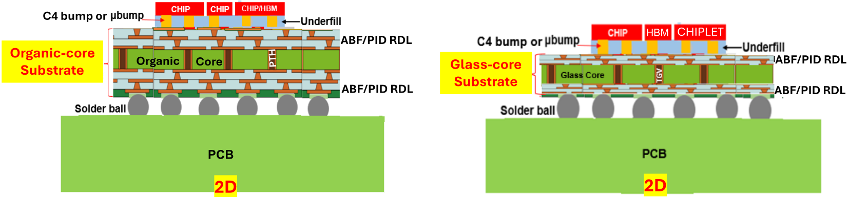
The key advantages of glass-core substrate over the organic-core substrate are:
- ➢Superior flatness
- ➢Better dimensional stability
- ➢Better heat resistance
- ➢Finer L/S RDLs
- ➢Cu-Cu hybrid bonding for chiplets
- etc.
Intel's Glass Packaging
On September 18, 2023, …
- ➢Intel has announceda new glass-substrate technology for the next generation of highpower processors.
- ➢Intel is on the path to delivering 1 trillion transistors on a package by 2030 and its ongoing innovation in advanced packaging including glass substrates will help achieve this goal.
Intel Glass Core Substrate
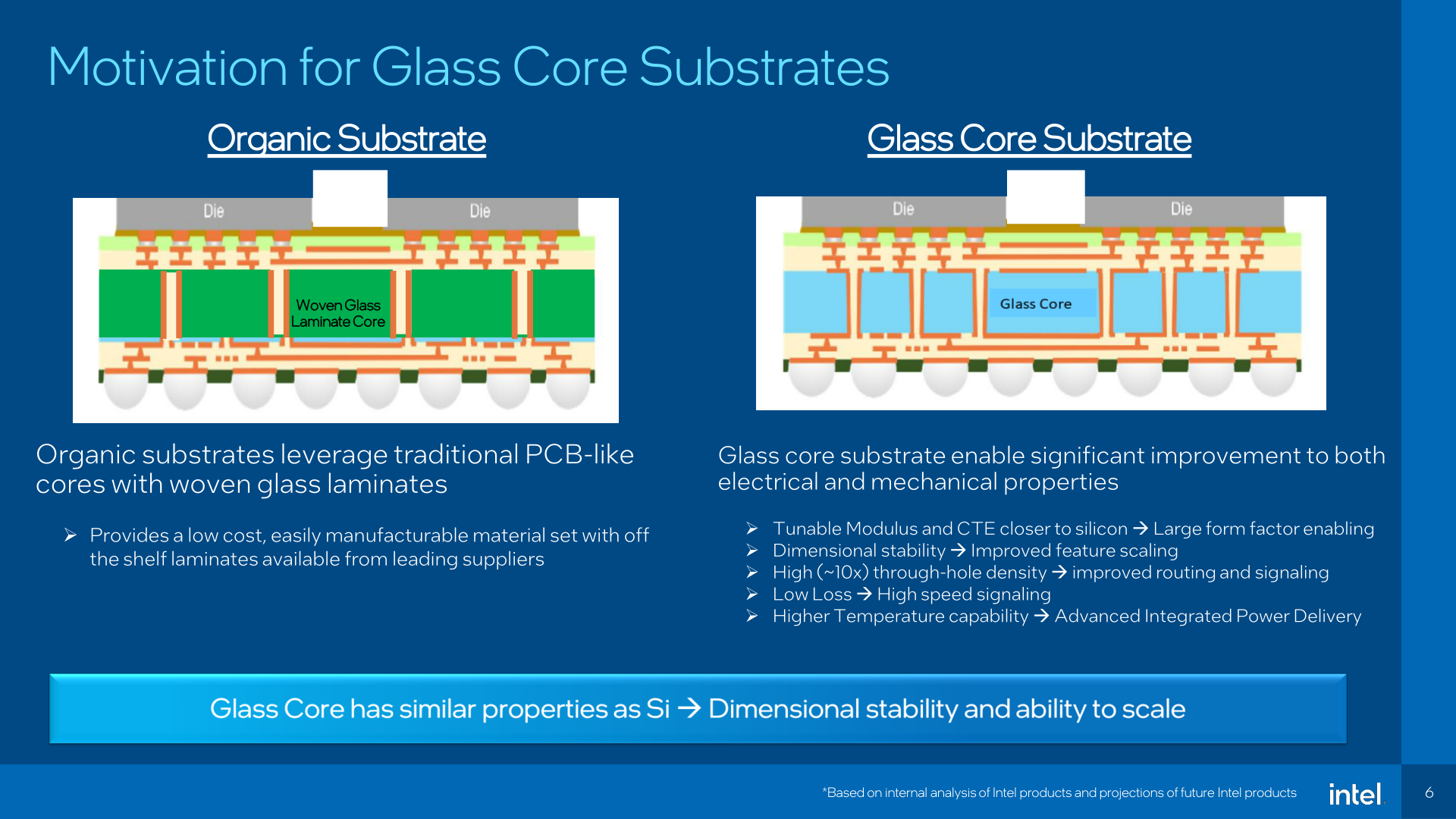
Organic Substrate
Glass Core Substrate
Compared to organic substrates, glass substrates offer:
*Based on internal analysis of Intel products and projections of future Intel products intel
- On September 18, 2023, Intel told the world that they had spent more than one billion dollars in glass packaging R&D. It is for their 1 trillion transistors on a package to be shipped by 2030
- During July 2025, Intel stopped all the in-house glass manufacturing activities and started licensing its extensive glass patents (> 700) to third suppliers.
- On July 28., 2026, Intel signed a memorandum of understanding with Lens International (HK) limited on how to fabricate crack-free through-glass via. 17
TSV Interposer vs. TGV Interposer
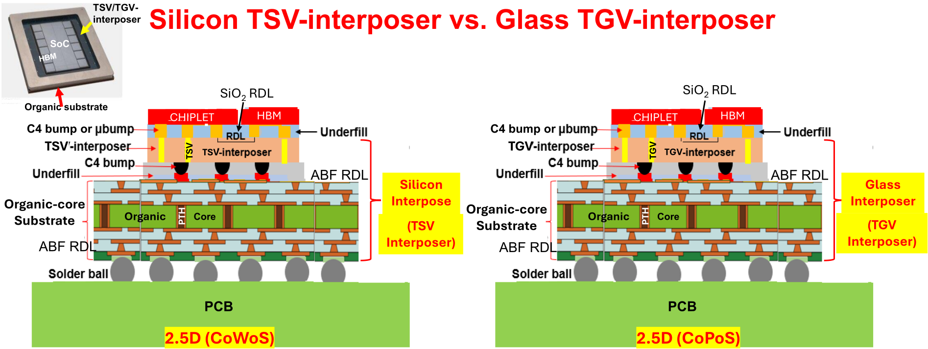
The key advantages of glass TGV-interposer over the silicon TSV-interposer are:
- ➢Better electrical isolation
- ➢Flatter surface
- ➢Lower D f and D k
- ➢Better area efficiency
- etc.
Package of Choice for HPC and Data Centers Driven by AI CoWoS (chip on wafer on substrate)
TSMC's Glass Packaging - CoPoS
During the TSMC 2025 North America Technology Symposium (April 23), the company announced its CoPoS (chip on panel on substrate) technology, which is competing with its CoWoS (chip on wafer on substrate) technology.
'310mm x 310mm Glass Panel'
There are many rumors on the CoPoSpackage structure!
Gag Order of CoPoS
For the very first time, in May 2026, TSMC issued a strict "gag order" and exclusivity mandate to its advanced packaging supply chain. This restriction targets companies involved in the panel-based CoPoS rather than the current-generation wafer-based CoWoS lines.
Nature of the "Gag Order" & Exclusive Agreements
Non-Disclosure Overhaul: TSMC is forcing Taiwanese materials, equipment, and manufacturing suppliers to sign aggressive legal agreements to ensure proprietary research and development secrets do not leak to rivals.
Mandatory Exclusivity: Beyond simple secrecy, the agreements act as a "lock-in" decree, legally barring these supply chain partners from selling the same CoPoS-generation tools or materials to any other semiconductor firms for several years during mass production.
The Strategic Intent
Blocking Intel and Samsung: Intel recently restarted advanced packaging expansions in Malaysia, and Samsung is heavily pitching its alternative solutions. Because some equipment manufacturers holding "TSMC Vendor Codes" began securing spillover orders from Intel, TSMC moved to legally choke off their access to next-gen supply lines.
Defending the Packaging Moat: Next-gen AI chips are hitting size ceilings on traditional silicon interposers. Rival tech like Intel's EMIB has started peeling away some market interest. TSMC intends to build an impenetrable barrier around CoPoS to prevent competitors from capitalizing on its multi-year R&D investments.
What's the package structure of CoPoS?
The tear-down of the first CoPoS product in Q1 of 2029 will tell!
I guess there could be three versions!
CoPoS (Chip on Panel on Substrate): v1
CoPoS (Chip on Panel on Substrate): v2
TSMC's CoWoS-L with Embedded
LSIs (Local Silicon Interconnects), i.e., Si-Bridges
CoWoS
CoWoS-L (Bridge with Fan-Out RDLs)
CoWoS (2.5D IC Integration) 27 TSV-Interposer is replaced by the RI (Reconstituted-Interposer) which consists of Si Bridge (LSI) embedded in Fan-Out EMC with fan-out RDLs
CoPoS (Chip on Panel on Substrate): v3
Bridge Embedded in Panel Fan-Out EMC with RDLs
CoPoS-v3
Interposers or Substrates Fabricated on a round wafer (WLP) and on a rectangular panel (PLP) -Area Efficiency.
- ➢WLP has been in high volume production for more than 25 years.
- ➢In the past few years PLP has been attracting lots of tractions. The one and only reason is PLP has better area efficiency (which leads to lower costs) compared to WLP.
- 31 ➢The larger the interposer (or substrate) size, the larger the area efficiency of the PLP (which leads to lower cost). This is very important for HPC and data centers in AI era. Because the interposer size is very large, e.g., 2500mm 2 (8HBM) or 3320mm 2 (12HBM). There are less than 10 physically possible interposers on a 300mm wafer.
Status CoPoS on
- TSMC has planned to establish its first CoPoS pilot line at Chiayi in 2026, with mass production facilities located at its P4 and P5 plants in AP7, Chiayi.
- Mat to trt et e s e s or eon
- The first wave of equipment supply chains has been largely finalized, with specifications and order volumes confirmed. These are:
- International companies: KLA, TEL, Screen, Applied Materials, and Disco
- Taiwanese companies: Innolux, Sin-Yun, Hung-Soo, Chung Hwa, Chromium, Chih-Sheng, and Da-Long
32 TSMC license some of Intel's glass patents and work with Ibiden and Innolux to make the TGVs and RDLs on a 310mm x 310mm glass panel.
TSV and RDLs
TSV Fabrication (Via-diameter = 5-10µm)
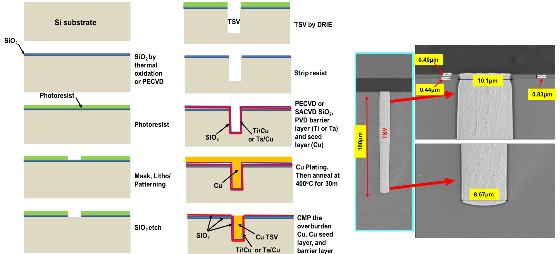
RDL Fabrication (Minimum Pitch = 0.4µm)
35 J. H. Lau, P. Tzeng, C. Lee, C. Zhan, M. Li, J. Cline, et al., 'Redistribution Layers (RDLs) for 2.5D/3D IC Integration', IMAPS 2013 Proceedings. Also, Journal of Microelectronic Packaging, First Quarter 2014, pp. 16-24.
TGV and RDLs
- ➢The TGVs are usually fabricated by the laser drilling such as the laser induced deep etching (LIDE) developed by LPKF Laser & Electronics AG in 2017.
- ➢The diameter of TGV in HPC and data centers in AI era is 20 - 50µm
- ➢The most common used glass materials are:
- SCHOTT AF 32 alkali-free flat glass
- CORNING HPFS 7980 high purity non crystalline fused silica glass
- Both materials have low CTE, which are close to that of silicon
(a) TGV sidewall metallization. (b) Cu plating. (c) An image of Cu-filled TGV
Metallization: Ti/Cu, electroless Cu, etc.
RDL Process Flow for (a) Glass Substrate (L/S ≥ 2µm), and (b) Glass TGV-interposer (L/S < 2µm)
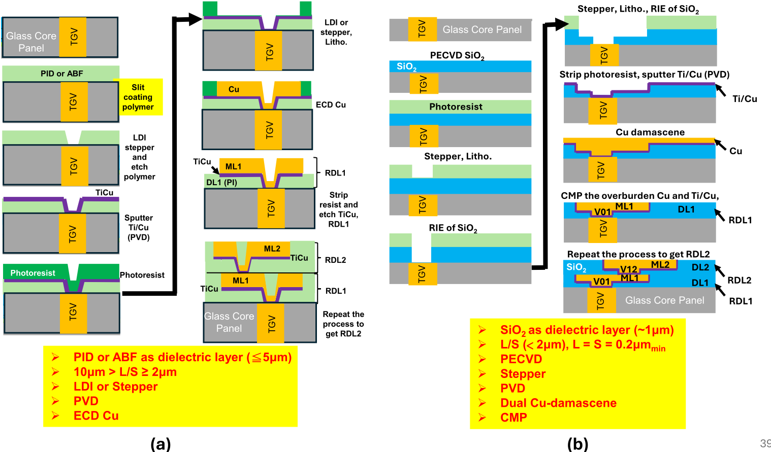
SEM image of glass-core substrate with TGV and RDLs (build-up layers) L/S > 2µm
RDLs (L/S = 0.2µm min ) on Top of Glass TGV-Interposer have not been published in the literature yet!
Process Compraison between the TSV and TGV
| Items | Through-Silicon Via (TSV) | Through-Glass Via (TGV) |
|---|---|---|
| Base Material | Silicon wafer | Alkali-free flat glass or fused silica |
| Via Formation | Deep Reactive-Ion Etching (DRIE) | Laser drilling / Laser Induced Deep Etching (LIDE) |
| Chemical Post-Processing | Gas-phase plasma etch chemistry | Anisotropic wet chemical etching (HF or NaOH) |
| Insulation Layer | SiO 2 (PECVD) | None - Glass is natively non-conductive |
| Metallization and Filling | Ti or Ta (PVD barrier layer) | Direct seed layer, e.g., Ti/Cu or electroless Cu |
| Sidewall Profile | Straight, vertical sidewalls. | Distinct taper angle (hourglass shape) |
| Via Filling | Electroplated with Cu | Electroplated with Cu |
| Maturity | Very | Not yet |
Mutuality Very Not yet but working on it
Standardization of Panel size for HPC and Data Centers in AI era
600mm x 600mm Panel vs. 310mm x 310mm Panel
Disadvantages
- ➢More expensive equipment
- ➢Larger floor space
- ➢Longer Pick and Place time
- ➢Larger warpage
- ➢Higher yield loss
- ➢Longer time to clean the equipment
- ➢The large panel must be cut into smaller panels for solder ball mounted
- ➢Etc.
Advantages
- ➢Higher area efficiency compared with 300mm-wafer
- ➢Similar process control as with 300mm-wafer
- ➢Similar yield loss as with 300mm-wafer
- ➢All the experience from 300mm-wafer can be adopted to 310mmx310mm panel
Cost! Cost! Cost!
Throughput & Processing Time Comparison: 300mm Wafer vs. 600mm x 600mm Panel
| Chip Size & Format | Approximate Die Count | Pick & Place (P&P) Time | Total Time (P&P + Molding) |
|---|---|---|---|
| 2mm × 2mm Chips | |||
| 300mm Wafer | ~16,684 chips | 100.1 minutes | 115.1 minutes |
| 600mm × 600mm Panel | ~88,209 chips | 529.3 minutes | 544.3 minutes |
| 3mm × 3mm Chips | |||
| 300mm Wafer | ~7,328 chips | 44.0 minutes | 59.0 minutes |
| 600mm × 600mm Panel | ~39,204 chips | 235.2 minutes | 250.2 minutes |
| 5mm × 5mm Chips | |||
| 300mm Wafer | ~2,592 chips | 15.6 minutes | 30.6 minutes |
| 600mm × 600mm Panel | ~13,924 chips | 83.5 minutes | 98.5 minutes |
- ➢Speed = 10,000 Units Per Hour (UPH) (0.36 seconds per chip)
- ➢Epoxy flow + Compression Molding time = 13 minutes
- ➢Since the P&P time is so long for 600mm x600mm panel, the compression molding machine has to be idle for a long time 45
Line Balancing: 300mm Wafer vs. 600mm x 600mm Panel
| 2mm x 2mm chip | 3mm x 3mm chip | 5mm x 5mm chip | |
|---|---|---|---|
| Time to populate 1 panel (min) | 529.3 | 235.2 | 83.5 |
| Time to populate 1 wafer (min) | 100.1 | 44 | 15.6 |
| Comp. Mold. Equi. idle time (%) for Panel | 94 | 88 | 78 |
| Required Panel P&P cluster size for no idling | 36 | 16 | 6 |
- ➢P&P Speed = 10,000 Units Per Hour (UPH) (0.36 seconds per chip)
- ➢Epoxy flow + Compression Molding time = 13 minutes
The Throughput Mismatch (1 P&P Machine : 1 Molding Machine)
➢2mm × 2mm Panel: (94% idle time). ➢3mm × 3mm Panel: (88% idle time). ➢5mm × 5mm Panel: (78% idle time). How Factories Fix This: Line Balancing For 2mm × 2mm Chips Time to populate 1 panel: 529.3 minutes Time to mold 1 panel: 15 minutes Required P&P cluster size: 36 P&P machines running in parallel. Result: Every 15 minutes, one of the 36 P&P machines finishes a panel and hands it off to the molding machine. The molding machine never idles. For 3mm × 3mm Chips Time to populate 1 panel: 235.2 minutes Time to mold 1 panel: 15 minutes Required P&P cluster size: 16 P&P machines running in parallel. Result: Every 15 minutes, one of the 16 P&P machines finishes a panel. For 5mm × 5mm Chips Time to populate 1 panel: 83.5 minutes Time to mold 1 panel: 15 minutes Required P&P cluster size: 6 P&P machines running in parallel. Result: Every 15 minutes, one of the 6 P&P machines finishes a panel. 47
Status of Panel Size
- ➢On April 23, 2025, TSMC announced they'll use 310mm x 310mm panel size for their CoPoS.
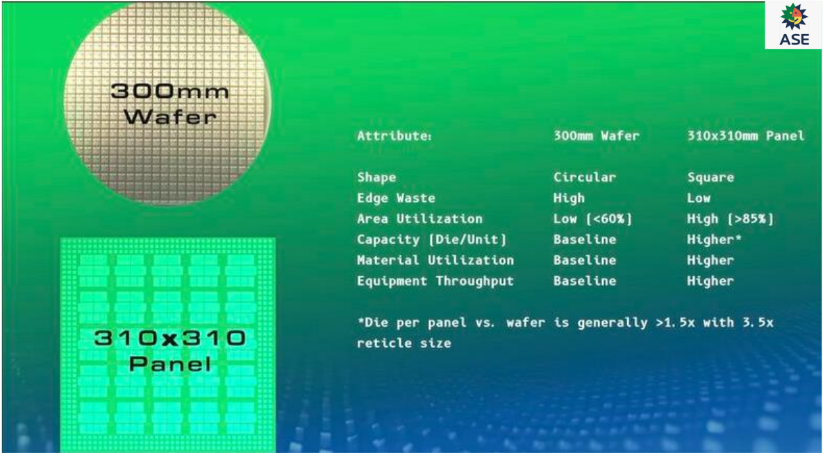
- ➢In March 2026, while ASE originally planned for a 600mm x 600mm panel line, it scaled back to310mm x 310mmto align with TSMC'spanel size. ASE aims to have a fully automated 310mm x 310mm production line operational for pilot production by theend of 2026.
- ➢On May 26, 2026, ASE formally announced the 310mm x 310mm panel size by the CEO (Dr. Tien Wu) of ASE at ECTC2026. Most of the successful experiences from 300mm wafer can be transferred to 310mm x 310mm.
- ➢With the #1 foundry (TSMC) and the #1 OSAT (ASE) now aligned, the market is poised to shift from experimentation to volume production.
- ➢Standardizing this panel size 310mm x 310mm is expected to help the entire semiconductor ecosystem scale AI chip packaging more reliably by providing a common platform for testing and manufacturing.
- ➢I do think that 310mm × 310 mm format strikes a critical balance: it is large enough to capture the area efficiency (cost) and small enough to maintain the processing control (yield). All the experience from 300mm-wafer can be adapted to 310mm x 310mm panel. 48
ASE's 310mm x 310mm
Flip Chip on Glass-core Substrate with µbumps
(Effects of glass-core substrate on Solder Joint Reliability)
Lau, J. H., N. Liu, M. Ma, and T. Tseng, 'Flip Chip on Glass-Core Substrates with Microbump and Cu-Cu Hybrid Bonding', Journal of Microelectronic Packaging, Vol. 22, Issue 3, September 2025, pp. 44-60.
Flip Chip (a) on organic-core substrate, and (b) on glass-core substrate
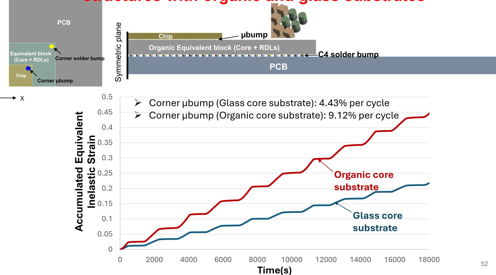
The chip dimensions are 10mm x 10mm x 350µm. The C4 bump is SAC. The µbump is Cu-pillar + Sn0.7Cu. Both solders obeyed Anand model. Build-up layers (RDLs) = 2 layers on top and 2 layers at the bottom. The thickness of each layer is 8µm (Cu metal layer = 3µm and dielectric layer = 5µm). The thickness of the glass core and organic core is 800µm. The thickness of the PCB = 1.57mm.
Maximum accumulated inelastic strain time-history in corner µbump of structures with organic and glass substrates
Y
joint of structures with organic and glass substrates Maximum accumulated inelastic strain time-history in corner C4 solder
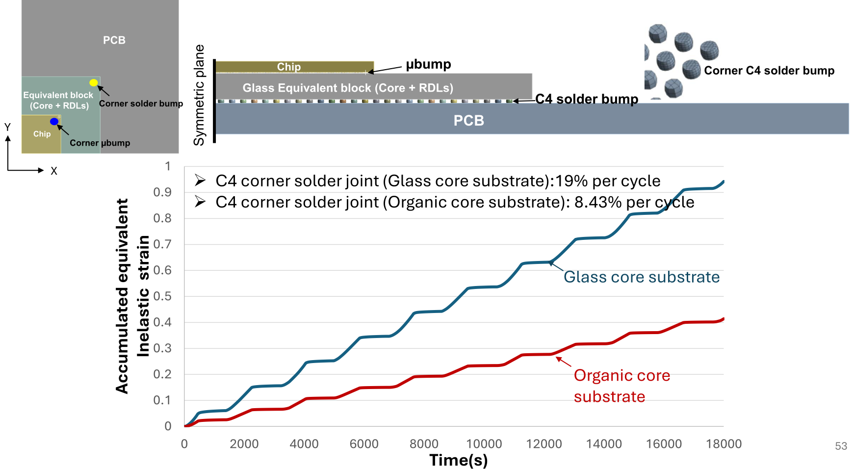
Max Accumulated equivalent inelastic strain: Glass-core Substrate vs. Organic-core Substrate
Y
X
| Interconnect Type | Organic Core Substrate (Max accumulated equivalent inelastic strain) | Glass Core Substrate (Max accumulated equivalent inelastic strain) | Technical Consequence / Status |
|---|---|---|---|
| Corner μbump Solder Joint with underfill | 9.12% per cycle | 4.43% per cycle | Low risk: Both are protected by underfill |
| Corner BGA Solder Joint without underfill | 8.43% per cycle | 19.0% per cycle | High risk: Glass core introduces more than doubles the inelastic strain on the PCB side where no underfill is presented |
C4 Solder Joint Reliability: Glass core vs. Organic Core
SUMMARY
As a matter of fact, the CTE of the glass substrate should be closer to the PCB CTE. Say 10x10 -6 / o C
.
Because there is underfill protection of the µbump solder joint on the glass substrate but there is no underfill protection for the C4 or BGA solder joints on the PCB.
Flip Chip on Glass-core Substrate with Cu-Cu Hybrid Bonding
(Effects of glass-core substrate on Solder Joint Reliability)
Cross section of flip chip on glass-core substrate with bumpless CuCu hybrid bonding
10mmx10mm
Equivalent Young's modulus, equivalent CTE, and equivalent
For Equivalent Young's modulus: 70.3GPa
121× 1.5∗4 +70× 1.5∗5 +72∗800
1.5∗4+1.5∗5+800
= 70.3GPa
For Equivalent Poisson's ratio: 0.29
0.34× 1.5∗4 +0.17× 1.5∗5 +0.29×800
1.5∗4+1.5∗5+800
= 0.29
For Equivalent CTE (Glass = 4.8): 4.85x10 -6 / o C
For Equivalent CTE (Glass = 10): 9.96x10 -6 / o C
Elastoplastic of dual-damascene copper
Finite element modeling of flip chip on glass-core substrate with Cu-
Cu hybrid bonding
Thermal cycling boundary condition
Deformation of structure with organic-core substrate.
85 O C (450s)_Side view
85 O C (450s)_Top view
-40 O C (2250s)_Side view
-40 O C (2250s)_ Top view
Time-history deformation of the structure
2250s Accumulated equivalent inelastic strain contours at the corner Cupads at 450s, 2250s, and 18000s
▪ 450s Accumulated equivalent (von Mises) stress contours at the corner Cupads at 450s and 2250s.
Accumulated equivalent inelastic strain contours at the corner solder ball at 450s and 2250s
Max
Time-history accumulated equivalent inelastic strain at the corner solder ball
Time(s)
20000
Warpage for glass-core substrate with CTE = 4.8x10 -6 / o C and 10x10 -6 / o C
Accumulated equivalent inelastic strain at the corner solder joint (CTE = 4.8x10 -6 / o C and 10x10 -6 / o C).
RECOMMENDATION
The CTE of Glass should be as close as to the PCB, instead of the Silicon chip.
3D Heterogeneous Integration of CPO (Switch, PIC and EIC) on Glass Substrate and Glass Interposer
3D Heterogeneous Integration of PIC and EIC with Glass Interposer and Cu-Cu Hybrid Bonding
Microbump
3.2T
3.2T
OE
Switch
ASIC
3.2T
OE
OE
3.2T
OE
3.2T
OE
OE
3.2T
OE
3.2T
OE
3.2T
OE
3.2T
OE
3.2T
TGV
Cu-Cu
EIC
ASIC switch Glass Interposer Fiber Coupler Fibers Glass Waveguide Glass Interposer Glass TGV- Interposer
145 140
142
155 184
143
TGV
PIC
125 144 160 186
165
PCB
µbump or
EIC
A
PD
Laser
Glass waveguide
RDL
Fiber Coupler
121
Fiber
125
120
123
Cu-Cu hybrid bonding
Underfill
3.2T
OE
OE
3.2T
OE
3.2T
OE
3.2T
OE
3.2T
X
Y
3.2T
OE
Underfill PCB
130
µbump
Switch
CPO substrate
115
115
US Patent No. 12,645,041, June 2, 2026, filed on April 1, 2024
PIC
PIC
Co-packaged optics substrate
Cu-Cu PIC
72
172(170)
Glass
waveguid
-110
3D Heterogeneous Integration of EIC and PIC by Cu-Cu Hybrid Bonding with the PIC Embedded in a Co-Packaged Glass Substrate
3.5D Heterogeneous Integration of Switch, PIC and EIC on Glass Interposer
3.5D Heterogeneous Integration of SoC, HBMs, Switch IC, PIC, and EIC on a TGV-Interposer in AI Era
In General, the Challenges of Glass Packaging are:
- ➢Micro-bubbles-free raw glass material formation
- ➢Crack-free TGV formation
- ➢Delamination-free seed layer formation
- ➢Fine L/S = 0.2µm min SiO 2 RDLs fabrication on top of TGV interposer
- ➢Fine 10µm < L/S ≥ 2µm ABF RDLs fabrication on both sides of glass-core substrate
- ➢RDLs thickness uniformity
- ➢Panel warpage for fabricating the RDLs
- ➢Handling
- ➢Testing
- ➢Integration within existing manufacturing environments
- ➢Immature technology
- etc.
SUMMARY and RECOMENDATIONS
- ➢FOWLP and FOPLP are not glass packaging.
- ➢Glass packaging either with a glass-core substrate or glass-core interposer is most suitable for HPC and date centers in AI era.
- ➢310mm × 310mm panel format strikes a critical balance: it is large enough to capture the area efficiency (cost) and small enough to maintain the processing control (yield). All the successful experience from 300mm-wafer can be adapted to 310mm x 310mm panel.
- ➢Because there is underfill protection of the µbump solder joint on the glass substrate but there is no underfill protection for the BGA solder joints on the PCB. Thus, for flip chip applications, the CTE of glass is recommended to be as close as to that of the PCB, e.g., 10x10 -6 / o C.
Some Recent Advanced Packaging Papers Published by the Lecturer and his Colleagues
- Lau, J. H., 'Recent Advances and Outlooks of Hybrid Bonding', IEEE Transactions on CPMT, 2027.
- Lau, J. H., and N. Liu, 'Silicon Bridges for Chiplets Heterogeneous Integration with Cu-Cu Hybrid Bonding' ASME Transactions, Journal of Electronic Packaging, 2027.
- Lau, J. H., N. Liu, T. Tseng, 'Microbump Reliability of Silicon Bridges for Chiplets Heterogeneous Integration', Journal of Microelectronic Reliability, Vol. 185, August 2026, pp. 116262.
-
Lau, J. H., 'Current Advances and Outlook of Advanced Packaging', ASME Transactions, Journal of Electronic Packaging, published online: February 11, 2026.
-
Lau, J. H., 'State-of-the-art and Outlooks of Cu-Cu Hybrid Bonding', IEEE Transactions on CPMT, Dec 2025, pp. 2575-2613.
-
Lau, J. H., 'Co-Packaged Optics - Heterogeneous Integration of Chiplets (Switch, Photonic IC, and Electronic IC)', J. of Microelectronic Packaging, V 22, Issue 4, Dec. 2025, pp. 93-104.
- Lau, J. H., N. Liu, M. Ma, and T. Tseng, 'Flip Chip on Glass-Core Substrates with Microbump and Cu-Cu Hybrid Bonding', J. of Microelectronic Packaging, V. 22, I3, Sept.2025, pp. 44-60.
- Lau, J. H., N. Liu, M. Ma, and T. Tseng, 'Flip Chip on Glass-Core Substrates with Microbump and Cu-Cu Hybrid Bonding', Journal of Microelectronic Packaging, 3 rd Quarter, 2025.
- Lau, J. H., N. Liu, M. Ma, and T. Tseng, 'Solder joint reliability - glass core substrate versus organic core substrate', Journal of Microelectronic Reliability, Vol. 168, May 2025, pp. 115701.
- 10.Lau, J. H., 'Current Advances and Outlooks in Hybrid Bonding', IEEE Transactions on CPMT, Vol. 15, No. 3, March 2025, pp. 651-681.
- 11.Lau, J. H., 'Co-Packaged Optics - Heterogeneous Integration of Photonic IC and Electronic IC', ASME Transactions, J. of Electronic Packaging, Vol. 147, March 2025, pp. 1-12.
- 12.Lau, J. H., 'State-of-the-art of Cu-Cu Hybrid Bonding', IEEE Transactions on CPMT, Vol. 14, No. 3, March 2024, pp. 376-396.
- 13.Lau, J. H, G. Chen, et al., 'Hybrid Substrates for Heterogeneous Integration' ASME Transactions, J. of Electronic Packaging, published online: Aug 11, 2023.
- 14.Lau, J. H, C. Lin, et al., 'Hybrid Substrate with Ultra-Large Organic Interposer for Heterogeneous Integration', IEEE Transactions on CPMT, Vol. 13, No. 9, September 2023, pp. 1371-1379.
- 15.Lau, J. H., 'Recent Advances and Trends in Chiplet Design and Heterogeneous Integration Packaging', ASME Trans., J. of Electronic Packaging, published online: June 23, 2023.
- 16.Lau, J. H., 'Recent Advanced and Trends in Cu-Cu Hybrid Bonding', IEEE Transactions on CPMT, Vol. 13, No. 3, March 2023, pp. 399-425.
- 17.Lau, J. H., 'Recent Advanced and Trends in Multiple system and Heterogenous Integration with TSV-Interposers', IEEE Transactions on CPMT, Vol. 13, No. 1, January 2023, pp. 3-25.
- 18.Lau, J. H., 'Recent Advanced and Trends in Multiple system and Heterogenous Integration with TSV-less Interposers', IEEE Trans. on CPMT, Vol. 12, No. 8, August 2022, pp. 1271-1280.
- 19.Lau, J. H., 'Recent Advances and Trends in Advanced Packaging', IEEE Transactions on CPMT, Vol. 12, No. 2, February 2022, pp. 228-252.
- 20.Lau, J. H., G. Chen, J. Huang, et al., 'Hybrid Substrate by Fan-Out RDL-First Panel-Level Packaging, IEEE Transactions on CPMT, Vol. 11, No. 8, August 2021, pp. 1301-1309.
21.Lau, J. H., 'State of the Art of Lead-Free Solder Joint Reliability', ASME Transactions, Journal of Electronic Packaging, Vol. 143, June 2021, pp. 1-36.
- 22.Lau, J. H., C. Ko, C. Lin, et al., 'Fan-Out Panel-Level Packaging of Mini-LED RGB Display', IEEE Transactions on CPMT, Vol. 11, No. 5, May 2021, pp. 739-747.
- 23.Lau, J. H., C. Ko, K. Yang, et al., 'Panel-Level Fan-Out RDL-first Packaging for Heterogeneous Integration', IEEE Transactions on CPMT, Vol. 10, No. 7, July 2020, pp. 1125-1137.
- 24.Lau, J. H., C. Ko, T. Tseng, et al., 'Panel-Level Chip-Scale Package with Multiple Diced Wafers', IEEE Transactions on CPMT, Vol. 10, No. 7, July 2020, pp. 1110-1124.
- 25.Lau, J. H., 'Recent Advances and Trends in Fan-Out Wafer/Panel-Level Packaging', ASME Transactions, Journal of Electronic Packaging, Vol. 141, December 2019, pp. 1-27.
- 26.Lau, J. H., M. Li, M. Li, et al., 'Fan-out wafer-level packaging for heterogeneous integration,' IEEE Transactions on CPMT, Vol. 8, Issue 9, September 2018, pp. 1544-1560.
- 27.Lau, J. H., M. Li, Q. Li, et al., 'Design, Materials, Process, and Fabrication of Fan-Out Wafer-Level Packaging', IEEE Transactions on CPMT. Vol. 8, Issue 6, June 2018, pp. 991-1002.
- 28.Lau, J. H., M. Li, Y. Li, et al., 'Warpage Measurements and Characterizations of FOWLP with Large Chips and Multiple RDLs', IEEE Transactions on CPMT, October 2018, pp. 1729-1737.
- 29.Lau, J. H., M. Li, D. Tian, et al., 'Warpage and Thermal Characterization of Fan-Out Wafer-Level Packaging', IEEE Transactions on CPMT, Vol. 7, Issue 10, October 2017, pp. 1729-1738.
- 30.Lau, J. H., 'Recent Advances and New Trends in Flip Chip Technology', ASME Transactions, Journal of Electronic Packaging, September 2016, Vol. 138, Issue 3, pp. 1-23.
- 31.Lau, J. H., Q. Zhang, M. Li, et al., 'Stencil Printing of Underfill for Flip Chips on Organic-Panel and Si-Wafer Substrates', IEEE Trans. on CPMT, Vol. 5, No. 7, July 2015, pp. 1027-1035.
- 32.Lau, J. H., 'Overview and Outlook of 3D IC Packaging, 3D IC Integration, and 3D Si Integration', ASME Trans, Journal of Electronic Packaging, Dec. 2014, Vol. 136, Issue 4, pp. 1-15.
- 33.Lau, J. H., C. Lee, C. Zhan, et al., 'Low-Cost Through-Silicon Hole Interposers for 3D IC Integration', IEEE Transactions on CPMT, Vol. 4, No. 9, September 2014, pp. 1407-1419.
- 34.Peng, C., J. H. Lau, C. Ko, et al., 'High-Density Hybrid Substrate for Heterogeneous Integration', IEEE Transactions on CPMT, Vol. 12, No.3, March 2022., pp. 469-478.
- 78 35.Lee, Z., J. H. Lau, CT Ko, et al., 'Characterization of Low-Loss Dielectric Materials for High-Speed and High-Frequency Applications', Materials Journal, 15, 2022, pp. 1-16.
- 36.Ko, CT, H. Yang, Lau, J. H., et al., 'Chip-First Fan-Out Panel Level Packaging for Heterogeneous Integration', IEEE Transactions on CPMT, 2018, V 8, Issue 9, Sept. 2018, pp. 1561-1572.
Some Packaging Books Published by the Lecturer and his Colleagues
- Lau, J. H., and K. N. Chiang, Cu-Interconnects, Glass, and AI-Assisted Simulation for Chiplets Heterogeneous Integration, (547 pages), Springer, New York, April 2026.
- Lau, J. H., and X. Fan, Hybrid Bonging, Advanced Substrates, Failure Mechanisms, and Thermal Management for Chiplets and Heterogeneous Integration, (645 pages), Springer, New York, April 2025.
- Lau, J. H., Flip Chip, Hybrid Bonding, Fan-In, and Fan-Out Technology, (501 pages), Springer, New York, 2024.
- Lau, J. H., Chiplet Design and Heterogeneous Integration Packaging, (525 pages), Springer, New York, 2023.
- Lau, J. H., Semiconductor Advanced Packaging, (498 pages), Springer, New York, 2021.
- Lau, J. H., and N. C. Lee, Assembly and Reliability of Lead-Free Solder Joints, (527 pages), Springer, New York, 2020.
- Lau, J. H., Heterogeneous Integrations, (367 pages), Springer, New York, 2019.
- Lau, J. H., Fan-Out Wafer-Level Packaging, (303 pages), Springer, New York, 2018.
- Lau, J. H., 3D IC Integration and Packaging, (458 pages), McGraw-Hill, New York, 2016.
- Lau, J. H., Through-Silicon Via (TSV) for 3D Integration, (487 pages), McGraw-Hill, New York, 2013.
- Lau, J. H., Reliability of RoHS compliant 2D & 3D IC Interconnects, (606 pages), McGraw-Hill, New York, 2011.
- Lau, J. H., C. K. Lee, C. S. Premachandran, and Yu Aibin, Advanced MEMS Packaging, (552 ages), McGraw-Hill, New York, 2010.
- Lau, J. H., C. P. Wong, N. C. Lee, and R. Lee, Electronics Manufacturing with Lead-Free, Halogen-Free, and Adhesive Materials, (643 pages), McGraw-Hill, New York, 2003.
- Lau, J. H., and R. Lee, Microvias for Low Cost, High Density Interconnects, (565 pages), McGraw-Hill, New York, 2001.
- Lau, J. H., Low Cost Flip Chip Technologies for DCA, WLCSP, and PBGA Assemblies, (585 pages), McGraw-Hill, New York, 2000.
- Lau, J. H., and R. Lee, Chip Scale Package: Design, Materials, Process, Reliability, and Applications, (564 pages), McGraw-Hill, New York, 1999.
- Lau, J. H., C. P. Wong, J. Prince, and W. Nakayama, Electronic Packaging: Design, Materials, Process, and Reliability, (498 pages), McGraw-Hill, New York, 1998.
- Lau, J. H., and Y. Pao, Solder Joint Reliability of BGA, CSP, Flip Chip, and Fine Pitch SMT Assemblies, (408 pages), McGraw-Hill, New York, 1997.
- Lau, J. H., edited, Flip Chip Technologies, (565 pages), McGraw-Hill, New York, 1996.
- Lau, J. H., edited, Ball Grid Array Technology, (636 pages), McGraw Hill, New York, 1995.
- Lau, J. H., edited, Chip On Board Technologies for Multichip Modules, (555 pages), Van Nostrand Reinhold, New York, March 1994.
- Lau, J. H., edited, Handbook of Fine Pitch Surface Mount Technology, (692 pages), Van Nostrand Reinhold, New York, 1994.
- Lau, J. H., edited, Thermal Stress and Strain in Microelectronics Packaging, (883 pages), Van Nostrand Reinhold, New York, 1993.
- Lau, J. H., edited, Handbook of Tape Automated Bonding, (645 pages), Van Nostrand Reinhold, New York, 1992.
- Lau, J. H., edited, Solder Joint Reliability: Theory and Applications, (631 pages), Van Nostrand Reinhold, New York, 1991.