260521_nmr_semi-renaissance
PDF 原檔:260521_nmr_semi-renaissance_original.pdf
原始內容
ANCHOR REPORT
Global Markets Research 21 May 2026
Greater China Semi
A guide to Semi renaissance in 2026-30F
As metal pitch scalability of advanced chips has not been able to keep up with demanding AI functions, we believe more transistor complexity and heterogeneous integration will be required. In our view, this will not only benefit Semi production equipment (SPE), but also the Semi material sector. We expect ALD (atomic layer deposition), etching, CMP (chemical mechanical planarization), wafer thinning, wafer-to-wafer/chip-to-wafer bonding, and materials related to photoresist, semi wafer, InP, SOI (silicon-on-insulator) wafer, glass core substrate to see strong growth over 2026-30F, as long as AI demand does not fade away. We initiate coverage with Buy ratings on AEMC (4749 TT), Kinik (1560 TT), and Ingentec (4768 TT); maintain our Buy ratings on Besi (BESI NA), Soitec (SOI FP), Dinglong (300054 CH), and Anji (688019 CH); and upgrade GWC (6488 TT) to Buy (from Neutral).
Key themes and analysis in this Anchor report:
- Updates on semi market trends and TSMC’s (2330 TT, Buy) localization plan ·
- High-NA EUV (high numerical aperture extreme ultraviolet lithography), metal-oxide resist and dry deposition/etching process ·
- 3D transistor, backside power delivery and SoIC (system on integrated chips) ·
- Wafer-bonded NAND and DRAM-on-logic ·
- InP (indium phosphide), photonics SOI, and glass core substrate ·
Research Analysts
Asia Technology
Donnie Teng - NIHK donnie.teng@nomura.com +852 2252 1439
Frank Fan - NIHK frank.fan@nomura.com +852 2252 2195
Aaron Jeng, CFA - NITB aaron.jeng@nomura.com
+886(2) 21769962
Anne Lee, CFA - NITB anne.lee@nomura.com
+886(2) 21769966
Eric Chen, CFA - NITB eric.chen@nomura.com +886(2) 21769965
Vivian Yang - NITB vivian.yang@nomura.com
+886(2) 21769970
Production Complete: 2026-05-20 21:56 UTC
EQUITY: TECHNOLOGY
Greater China Semi
EQUITY: TECHNOLOGY
A guide to Semi renaissance in 2026-30F
Revolution in Semi materials, spare parts and SPE being driven by rapid migration in advanced technology
When metal pitch scalability can’t keep up with demanding AI functions, more transistor complexity and heterogeneous integration are required
AI infrastructure and Agentic AI demand are driving evolution of already fast-moving Semi technologies at a speed that has never been seen before in history. We believe advanced node migration alone can’t fulfill the requirements from all perspectives, which include not just computing performance, but also more efficient power saving, better heat dissipation, wider data process bandwidth, faster electrical and optical signal transmission speed, and more responsive reaction time at the physical AI interfaces. As a result, in our view, complicated 3D transistor designs and backside power delivery (BPD), with heterogeneous integration and different types of materials have quickly started playing a more important role. We believe this is changing the landscape of the Semi market’s growth that used to be mainly driven by transistor pitch scalability, which primarily follows the Moore’s Law. We initiate coverage with Buy ratings on AEMC, Kinik, and Ingentec; maintain Buy on Besi, Soitec, Dinglong, and Anji; and upgrade GWC to Buy (from Neutral).
Photoresist and lithography process upgrade is necessary when high-NA EUV is available in the market
With a higher NA (numerical aperture) light source, the thinner photoresist layer reduces the risk of pattern collapse, but also requires more advanced photoresist material that can better capture photons, with an improved etching process. As a result, we believe this will lead to the adoption of new metal-oxide resists (MOR), while dry deposition and etching could replace the existing wet process. In our view, from TSMC’s perspective, Lam Research (LRCX US, Not rated) could be the ultimate winner as it can provide dry deposition and etching equipment with JSR (unlisted) being the major supplier of MOR material. We expect this will increase the total addressable market (TAM) for photoresist and photoresist auxiliary due to the upgrade in materials.
3D transistor, BPD and SoIC will play more important role
Besides pitch scalability, we believe the Semi industry is focusing more on device/transistor structure innovation, particularly on more complicated 3D transistors, such as the current gate-all-around FET (GAAFET); while in the future, transistors will be stacked on top of each other which is called a complementary FET (cFET) device. At the same time, BPD has also been introduced that allows both additional space for logic transistors and power saving. While a SoIC (system on integrated chips) leaves room for design flexibility so that IC designers can vertically integrate ICs with different functions. We expect ALD, etching, CMP, wafer thinning, wafer-to-wafer bonding and chip-to-wafer hybrid bonding demand to grow rapidly. Hence, in our view, Semi wafer consumption would increase as well.
Wafer-bonded NAND and DRAM-on-logic to improve the performance of memory
Density and bandwidth requirements are growing considerably across memory hierarchies in both cloud and physical AI applications. A wafer-bonded NAND increases the NAND storage density per memory die while the DRAM-on-logic unlocks the memory bandwidth between DRAM and a logic SoC. Hence, we believe the demand for CMP, wafer thinning, and wafer-to-wafer bonding should grow, along with more Semi wafer consumption.
Combinations of materials are critical in SiPh and glass core substrates
Materials such as silicon photonics (SiPh) and glass core substrates have quickly emerged to meet the demand for AI networking. SiPh makes a compact optical transceiver with better integration and scalability, while glass core substrates achieve better heat dissipation and lower warpage. Hence, the demand for multiple materials such as InP, photonics SOI and glass core substrates should grow rapidly, in our view.

Research Analysts
Asia Technology
Donnie Teng - NIHK donnie.teng@nomura.com +852 2252 1439
Frank Fan - NIHK frank.fan@nomura.com +852 2252 2195
Aaron Jeng, CFA - NITB aaron.jeng@nomura.com
+886(2) 21769962
Anne Lee, CFA - NITB anne.lee@nomura.com +886(2) 21769966
CW Chung - NIHK cwchung@nomura.com +852 2252 6075
Eric Chen, CFA - NITB eric.chen@nomura.com +886(2) 21769965
Vivian Yang - NITB
vivian.yang@nomura.com +886(2) 21769970
Japan technology
Manabu Akizuki - NSC manabu.akizuki@nomura.com +81 3 6703 1185
Atsushi Yoshioka - NSC
atsushi.yoshioka@nomura.com +81 3 6703 1176
Virginia Wang - NSC virginia.wang@nomura.com +81 3 6703 1215
Japan chemicals & textiles
Shigeki Okazaki - NSC shigeki.okazaki@nomura.com +81 3 6703 1170
Daiki Ban - NSC daiki.ban@nomura.com +81 3 6703 1124
Ticker
Semi materials
4768 TT
4749 TT
4772 TT
4186 JP
5234 TT
DD US
BAS GR
AI FP
Mean
APD US
Median
1560 TT
ENTG US
8028 TT
MMM US
300054 CH
6140 JP
688019 CH
Mean
Median
6488 TT
688126 CH
SOI FP
3532 TT
002428 CH
AXT US
Mean
Median
Advanced Echem Materials
Fig. 1: Stocks for action
Rating
Buy
Buy
Not Rated
PIE (x)
2026F
2027F
68.4
n.a.
41.5
54.4
105.3
31.4
Mkt Cap
USDmn
2,917
628
1,368
Current Price
(LC)
1,015.0
430.5
299.5
P/S (x)
2026F
2027F
17.7
11.1
11.2
14.1
7.9
8.9
P/B (x)
2026F
2027F
9.5
13.6
10.7
8.8
2.2
8.6
9.2
31.7
| Company | Code | Rating | Market Cap (USD mn) | Avg. TO (USD mn) | TP (LCY) | 15-May (LCY) | Upside (%) |
|---|---|---|---|---|---|---|---|
| Ingentec* | 4768 TT | Buy | 767 | 25 | 960 | 431 | 123% |
| Soitec | SOI FP | Buy | 6,883 | 148 | 250 | 148 | 69% |
| AEMC* | 4749 TT | Buy | 3,206 | 78 | 1500 | 1,015 | 48% |
| Dinglong | 300054 CH | Buy | 10,128 | 285 | 104 | 73 | 43% |
| Kinik* | 1560 TT | Buy | 2,685 | 45 | 840 | 629 | 34% |
| Besi | BESI NA | Buy | 24,395 | 150 | 340 | 262 | 30% |
| Anji Microelectronics | 688019 CH | Buy | 7,425 | 145 | 360 | 289 | 25% |
| GlobalWafers | 6488 TT | Buy | 12,209 | 115 | 850 | 710 | 20% |
8.0
6.3
41.0
Note: Stocks on which we are initiating coverage in this Anchor report are marked with an *; closing price as on 15 May 2026 Note 2: n.a. 91.1 3.5
Source: Bloomberg Finance L.P., Nomura estimates
Ingentec: Leading specialty gas supplier with (Through-Glass Via) TGV capability in Taiwan
AEMC: Leading photoresist and photoresist auxiliary supplier in Taiwan
Soitec: Largest SOI wafer company in the world
Dinglong: Leading CMP-related material supplier in China
Besi: Leading hybrid bonding tool company in the world
Kinik: Leading CMP pad conditioner and reclaim wafer supplier in Taiwan
Anji Microelectronics: Leading CMP-related material supplier in China
GlobalWafers: Third largest Semi wafer supplier in the world
Fig. 2: Valuation comparison table
Note: Bloomberg consensus for Not rated stocks; data as on 15 May 2026
Source: Bloomberg Finance L.P., Nomura estimates
6.3
56.7
56.2
24.9
12.3
n.a.
35.5
52.7
22.6
12.4
n.a.
94.5
407.2
n.a.
180.9
94.5
171.9
n.a.
164.61
n.a.
114.8
127.9
4.6
n.a.
n.a.
38.6
12.5
4.0
7.0
2.9
3.3
4.6
n.a.
n.a.
36.6
11.9
4.0
ROE (%)
2026F
2027F
14.4
(1.5)
29.5
28.2
16.0
6.7
6.8
14.9
17.8
14.8
14.9
22.8
12.9
23.3
89.8
4.8
‘6.1
28.2
28.3
22.8
8.6
(4.4)
(0.3)
3.6
3.3
5.2
2.7
16.8
3.2
36.2
27.2
16.5
7.0
7.7
15.3
17.7
16.4
16.5
24.2
15.0
25.1
79.1
4.8
15.8
30.0
27.7
24.2
10.6
3.7
1.2
n.a.
5.8
7.0
5.7
5.8
EV/Sales (x)
2026F
2027F
17.5
10.4
11.5
7.6
4.8
3.2
1.1
4.0
6.7
7.4
6.7
9.7
6.9
8.8
3.4
1.2
15.4
15.3
8.7
8.8
5.5
8.7
17.2
7.8
57.0
56.7
25.5
13.0
14.0
5.2
9.1
8.1
4.3
3.1
1.11
3.8
6.3
6.1
5.2
8.3
6.1
7.0
3.3
1.1
12.1
12.3
7.2
7.0
4.7
7.9
13.4
n.a.
35.7
53.1
22.9
13.4
0.8
0.9
1.7
1.9
0.8
1.6
4.3
2.2
2.5
1.9
1.7
0.8
0.3
1.5
2.2
2.5
n.a.
0.3
1.3
1.1
1.1
0.0
0.0
0.9
n.a.
n.a.
0.5
0.5
1.0
0.7
2.3
2.8
0.9
1.7
4.5
2.4
2.5
2.1
2.3
0.8
0.3
2.0
2.3
2.7
n.a.
0.3
1.4
1.4
1.6
0.0
0.0
n.a.
n.a.
n.a.
0.5
0.0
2026
2027
Executive summary
Mentioned in this report
Yes
Guide to the evolution of key Semi processes and materials in 2026-30F
AI infrastructure and Agentic AI demand are driving the evolution of already fast-moving Semi technologies at a speed that has never been seen before in history. The advanced node migration alone can’t fulfill the requirements from all perspectives, which include not just computing performance, but also more efficient power saving, better heat dissipation, wider data process bandwidth, faster electrical and optical signal transmission speed, and more responsive reaction time at the physical AI interfaces. As a result, in our view, 3D transistor design and BPD, with heterogeneous integration across 2.5D/3D packaging and different types of materials have quickly started playing a more important role. We believe this is changing the landscape of Semi market growth that used to be mainly driven by transistor density growth, which follows the Moore’s Law. But it is slowing down quickly, particularly when the next-generation EUV and high-NA EUV are not likely to be widely adopted by the Semi industry until 2029-30F at the earliest, in our view. In this report, we will discuss the evolution of most key Semi technologies over 2026-30F (Fig. 3 - 4 ).
Fig. 3: Evolution of key Semi technologies in 2026-30F
Source: Nomura research
2028
2029
2030
Fig. 4: Key Semi technologies, market growth, beneficiaries, and timeline
| Technology | 2025-2030 | Key Equipment | Key Materials | Major Beneficiaries | Note |
|---|---|---|---|---|---|
| GAA(Gate-All- Around) | CAGR >20% | ALD (Atomic Layer Deposition) Selective Etch Epitaxy (Si/SiGe Superlattice) CMP Metrology / Inspection | High-k Dielectrics (HfO₂) SiGe Superlattice Wafers Work-Function Metals (TiN, TiAl) Molybdenum (contact metal) Metal Oxide Resists | ASMInternational, Applied Materials,Lam Research, Tokyo Electron, KLA Tencor | CAGRof over 20%as part of the normal advanced node migration. Will start growing from 2026F. |
| SoIC (System on Integrated Chip) | >30% | Hybrid Bonder (D2W) TSV Etch &Fill Wafer Thinning/CMP Temp. Bond / Debond Optical Inspection RDL Deposition | Cu-Cu Bonding Interfaces SiCN / SiO₂ Dielectrics CMPSlurries (Cu) Underfill Materials | BESI, Applied Materials, Ebara, Disco, Onto Innovation, Camtek | CAGRof over 30%due to the very low base in 2025;we expect it to rapidly increase in 2026-27F due to TSMC’s SoIC capacity expansion and potential adoptionbyHBM customers. Will start growing from 2026F. |
| Glass Core Substrate | >40% | TGV Laser Drill / Etch Panel-Level Lithography RDL / Metallization (Sputter, Plate) Glass Panel Handling Metrology (Warpage, Defect) | High-Purity Glass Panels Cu / Ti / WMetallization ABF-type Dielectric Films CMPSlurries (Glass) | Ibiden, Unimicron, SEMCO, Toppan Absolics (SKC), JNTC, LG Innotek, Ingentec LPKF, DRLaser, E&R Engineering, Innostar Service Schott, AGC, Corning | CAGRof over 40%as it’s a totally new technology/material. Will start growing from 2027F at the earliest. |
| Backside Power Delivery (BSPDN) | >20% | Nano-TSV Etch &Fill Wafer Thinning/CMP Carrier Wafer Bonding Backside Litho (DUV / EUV) Backside Metal Deposition EDA Tools (P&R re-design) | CMPSlurries &Pads Cu / Ru / MoInterconnects Low-k Dielectrics Carrier Wafer Adhesive | Disco, Ebara, Applied Materials, EVG, TEL, SUSS Microtec, Entegris, CMCMaterials, Kinik,3M | CAGRof over 20%as part of the normal advanced node migration. Will start growing from 2027F. |
| Wafer Bonded NAND(Xtacking- type) | >20% | W2WHybrid Bonder High Aspect Ratio Etch (60:1+) ALD / CVD(multi-layer stack) CMP(post-bond planarize) Optical Inspection | SiO₂ / SiN Multi-Layer Stacks W/Mo(Wordline metals) Cu-Cu Bonding Interface Polysilicon Channels | EVG, TEL, SUSS Microtec, LamResearch,AMEC | CAGRof over 20%as part of the normal NANDproduction technology migration. Will start growing from 2027F. |
| DRAM-on-Logic (LPDDRW2W) | >30% | W2WHybrid Bonder TSV Etch &Fill ALD (High-k Capacitor) Wafer Thinning / Grinding Advanced Litho (EUV for Logic) Metrology (Alignment) | High-k Capacitor Dielectrics (ZrO₂, HfO₂) IGZO / Oxide Channels (future) Cu-Cu Bonding Interface Ru / MoInterconnects | EVG, TEL, SUSS Microtec | CAGRof over 30%as we believe it would not pick up meaningfully until 2028F driven by edge AI/physical AI applications. Will start growing from 2028F. |
| InP-Based Lasers | >20% | MOCVD/MBEEpitaxy III-V Wafer Processing Facet Coating / Cleaving Die Bonding / Packaging Burn-In &Reliability Test | InP Substrates (2”→6”) InGaAsP / InGaAlAs Epitaxy High-Purity Indium &Phosphorus AR/HR Coatings | Lumentum, Coherent (II-VI) Sumitomo Electric, AXT, JX Metals Landmark, VPEC, Win Semi, IQE Aixtron | CAGRof over 20%as we believe growth can reach very high in 2025- 27F, but moderate in 2028-30F if more meaningful capacity is built across the industry, particularly in China. Will start growing from 2026F. |
| Photonics SOI (SiPh) | >30% | SOI Wafer Fab (DUV Litho) Ge Epitaxy (Photodetectors) Edge / Grating Coupler Fab Wafer Bonding (InP-on-Si) CPOPackaging Tools | Photonic SOI Wafers (220nm/400nm Si) SiN (Low-Loss Waveguides) Ge (Photodetectors) LiNbO₃ (Modulators, emerging) | Soitec, GlobalWafers, NSIG/Simgui, Shin-Etsu | CAGRof over 30%, which is higher than that of InP material, as Photonics SOI’s (SiPh) growth momentumwill start later than that for InP substrate, mainly driven by SiPh used in CPOafter 2027F. Will start growing from 2027F. |
| High-NAEUV | >40% | High-NA EUV High-Power EUV Light Source Anamorphic Optics &Mirrors Metal Oxide / Dry Deposition NewReticle / Mask Infrastructure Advanced Metrology and Overlay | Metal Oxide Photoresist (MOR) EUV Pellicles Ru-capped Multilayer Mirrors Ultra-Low-Defect EUV Mask Blanks Hydrogen Gas Dry Resist Chemicals | ASML Carl Zeiss, Trumpf, AGC/Mitsui, Hoya/AGC, JSR/Inpria, LamResearch,AEMC KLA Tencor/Lasertec, Guden/Entegris | CAGRof over 40%depending on whether TSMCwill adopt high-NA EUV on A10 node or further push it out. Will start growing from 2029F at the earliest. |
Source: Nomura research
Lalgel tie
70
cultaul ar eao, wollel tlle vowel bullouttiytiull
3D transistor, BPD, and advanced packaging such as SoIC and CoWoS/CoPoS will play more important role
60
50
40
30
20
10
0
We believe the Moore’s Law may still continue along with the pitch to scale down further once the leading Semi companies start adopting high-NA EUV at around 1nm (A10). In this case, we think the Semi market giants, such as ASML (ASML US, Not rated) and TSMC, could still be able to widen their technology leadership over other Semi companies in the next decade. However, in our view, if high-NA EUV eventually proves to be less cost effective and is pushed out further, pitch scaling could no longer remain a key topic in the future, where the whole Semi industry will focus more on device/transistor structure innovation, from 2D to 3D structure and transistors that are stacked on top of each other, called a cFET device, compared to the current GAAFET type.
Fig. 5: Metal pitch scaling - historical trend
N16 N10
Source: Nomura estimates, IMEC
Fig. 6: Contact area between gate and source/drain electrodes
Larger the contact areas, better the power consumption
Source: Samsung, Nomura research
(Nanowire, Nanosheet, Forksheet)
Oxide
The approach to fabricate stacked-Si nanowires for GAA (gate-all-around) devices in Fig. 7 includes: 1) a stack of Si/SiGe layers grown on a silicon wafer; 2) anisotropic plasma etching (vertical direction) achieved in an inductively coupled plasma (ICP) reactor; 3) isotropic and selective etching (both vertical and horizontal directions) of SiGe layers in an RPS (remote plasma source) reactor; 4) the cycle of a two-step process alternating oxidation (atomic layer deposition; ALD) and etch; and 5) the release of horizontal Si nanowires. As a result, we believe the deposition and etching processes will be increasing more meaningfully. Si substrate nanowires
SIO, BOX 20 nm
Si substrate

Source: Journal of Vacuum Science & Technology A Vacuum Surfaces and Films, Nomura research
A power delivery network is designed to provide power supply and reference voltage to the active devices on a die most efficiently. A BPD network decouples the power delivery network from the signal network by moving the entire power distribution network to the backside of the silicon wafer, which today serves only as a carrier. From there, it enables direct power delivery to the standard cells through wider, less-resistive metal lines, without the electrons needing to travel through the complex BEOL stack. This approach promises to benefit the IR drop, improve the power delivery performance, reduce routing congestion in the BEOL, and when properly designed, allow for further standard cell height scaling.
As two silicon wafers will be used in the back-side power delivery process, one being the silicon wafer acting as an interposer in between the signal network, and another acting as the permanent silicon carrier of the device, we expect the usage of silicon wafers to increase along with wafer bonding. On the other hand, we believe the wafer bonding, CMP, grinding and thinning process will increase as well to form the silicon interposer in between the signal and power network.
Isotropic etching in RPS reactor: cycle of a two-step process
Oxidation
Etch
Oxidation
Etch
wIlNI
Fig. 8: Process flow of BPD
STEP 2
Permanent bonding
STEP 3
Backside passivation
Source: IMEC, Nomura research
An alternative solution to the high-NA EUV stitching issue is the avoidance of large dies altogether. In advanced packaging such as SoIC, by using hybrid bonding technology, it has been proven that it is possible to maintain high performance even while separately fabricating parts of circuits that previously had been fully integrated into a single die. This is currently being done to improve the cost-effectiveness of advanced lithography. For example, the high-performance logic circuits of AMD’s (AMD US, Not rated) EPYC processor have been fabricated using 7 nm technology, while input/output functions have been fabricated using lower-cost 14 nm processes. In other applications, memory access rates are improved using advanced packaging technology. It may also be possible to achieve high levels of performance with maximum die sizes that can fit into the exposure fields of high-NA EUV exposure tools.
Fig. 9: Chip-to-chip/wafer hybrid bonding
Source: Nomura research
Chip 5
Chip 6
Chip 7
HiT i Tin
Oxide-oxide direct
Cu
Oxid
Memory
Cell Array
CMOS wafer metal VIAs(Vertical Interconnect Accesses)
Memory wafer
Cell array
Wafer-bonded memory (wafer-bonded NAND; DRAM-on-logic) to maximize performance and bandwidth
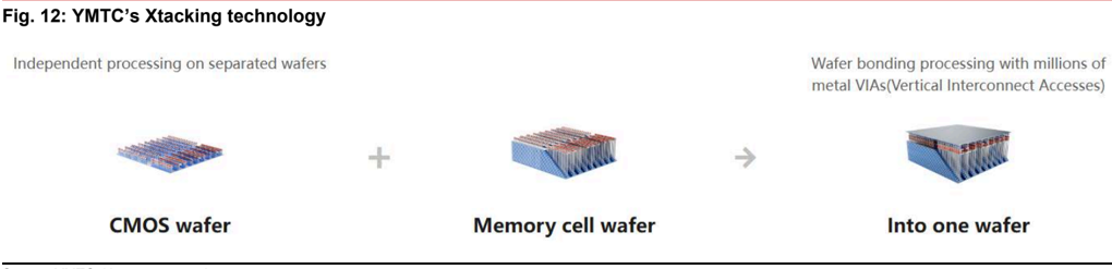
Bit line
The wafer-bonded NAND technology was introduced by YMTC (unlisted) for the first time in 2018. YMTC’s wafer-bonded technology is called Xtacking, and can also be called CMOS directly bonded to array (CBA) technology, which makes it possible for the CMOS circuit (logic) wafers and memory cells array wafers to be manufactured separately and bonded together. Before the launch of CBA architecture, 3D NAND architectures in the market were divided into traditional side-by-side structure and CnA (CMOS next to Array) architecture.
Word line hook up interconnect
Cu bonding pad
Bonding interface
CMOS
Since the two types of wafers are manufactured in parallel, there is also the added benefit of shortened production times compared to the conventional method. Performing hightemperature processing solely on the memory cell array wafer makes it possible to achieve the optimal temperature to ensure reliability without having to consider the impact on the CMOS circuit. By separating the wafer manufacturing processes, the performance of the CMOS circuit and the memory cell array can be maximized.
Fig. 10: 3D NAND: CNA vs CBA structure
Source: Kioxia, Nomura research
Source: YMTC, Nomura research
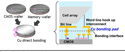
AI inference is a memory-bound task in the smart-edge domain requiring high memory bandwidth and energy efficiency with modest computing power between 45 and 100+ TOPS (trillions of operations per second). The DRAM-on-logic WoW can achieve 1TB/s bandwidth for throughput higher than 100 TPS (tokens per second). We believe the strong momentum for DRAM-on-logic could start from 2028F, led by AI agents in automotive smart cockpit, premium smartphones/PCs, and robotics.
Fig. 11: Wafer-to-wafer bonding structure
Source: Kioxia, Nomura research
Into one wafer
nm module)
WoW (WoW hybrid bonding, no interposer
0.55 NA EUV
>>10X higher etch and bump)
building blocks
0.33 NA EUV
4X more photons absorbed / volume
Source: Nomura research
Resist
Transfer layer selectivity & contrast
Si
Photoresist upgrade is critical along with high-NA EUV to drive further scalability of metal pitches
With a higher NA, photons strike the wafer at a shallower angle. That requires thinner photoresist layers to avoid shadowing. The upside is that a thinner resist layer reduces the risk of pattern collapse, as the aspect ratio of resist features is smaller. However, it also provides less protection for the wafer. In addition, long etch processes used to create high-aspect ratio wafer features can erode the resist layer, ultimately degrading the transferred pattern. With less material, a thinner resist also captures fewer photons, potentially making roughness and other stochastic effects worse.
At present, metal-oxide resists are probably the leading alternative to photoacid-driven chemistries, or chemically amplified resists (CAR). Based on a metal-oxide core, surrounded by ligands that tune solubility, crosslinking, and other properties, these resists offer inherently good etch resistance. The dense core absorbs more energy, too, attenuating electron energy and reducing blur.
Fig. 14: Reduction in photoresist film thickness
Source: Cadence, Nomura research
material
Schott
AGC
Corning
Laser Modification
Etching
Through Glass Etching
AOL
Glass Inspection
Electroless plating
Seed Layer Coating
Sputtering
Seed Layer Coating
Electroplating or copper pillar mass
transter
Double-Sided Copper
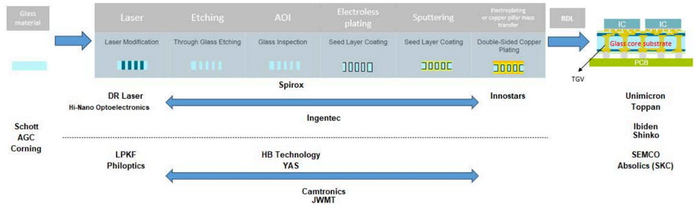
Glass core substrate is an emerging new technology amid rising demand for optical communications and tight ABF substrate supply
Glass core substrates and interposers are being pursued intensively by leading device makers, materials suppliers, and equipment vendors for advanced packaging applications. Intel (INTC US, Not rated) has publicly demonstrated its glass core substrates for next-generation advanced packaging, positioning the work as foundational research for the latter part of this decade rather than imminent high -volume manufacturing, which helps frame expectations for the technology’s maturity today. We believe Broadcom (BRCM US, Not rated) is likely one of the early movers of adopting glass core substrates by 2027F at the earliest, which may be firstly adopted on its switch ASIC. We think the main reason that Broadcom is considering the use of glass core substrates is mainly to avoid the heat issue which could result in the warpage of substrates. Using the glass core substrate (a good heat spreader) will lead to better heat dissipation through copper pillars, in our view. However, we see two uncertainties for the glass core substrate adoption in the coming year: 1) substrate makers are still dealing with the RDL dielectric peeling and delamination issue; 2) ABF substrate and EMIB-T demand is too strong for substrate makers to invest in glass core substrate capacity.
Fig. 16: Process of glass substrate and some supply chain names related to Broadcom
Source: Manz, Nomura research
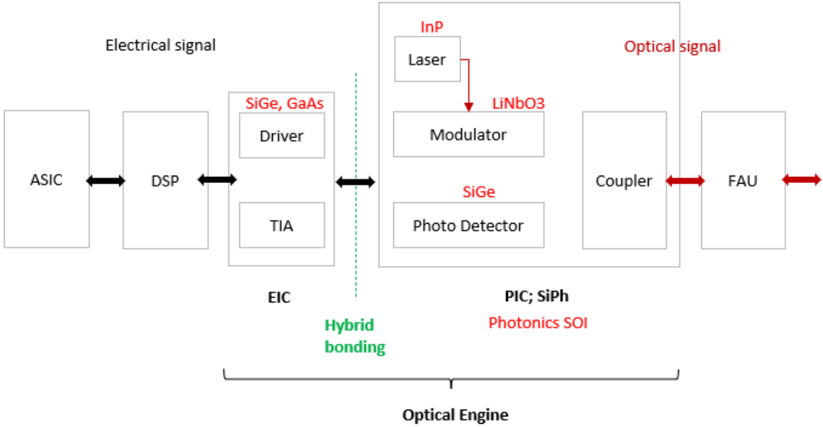
The fast-growing optical communications market is driving surging demand for InP substrate and photonics SOI wafers
Driven by global AI leaders’ buoyant demand for high-speed optical transceivers, as well as persistent component shortages (i.e., optical chips), we believe the product upcycle will continue into 2027F. Meanwhile, product innovation in the optical transceiver market is accelerating, and future technology trends including silicon photonics (SiPh), LPO/LRO, and NPO/CPO primarily target higher performance, lower energy consumption and costs. We believe the 1.6T upgrade and SiPh migration are the key drivers. We also think NPO/CPO technologies will continue to improve. In our view, if leading CPO solution providers use bundled sales strategies for their CPO switch products, then it could accelerate adoption rates in a scale-out network in the medium term, while there are more CPO use cases for the scale-up network in the long term.
Other than using silicon-based wafers to produce key ICs in optical transceivers, other critical areas where non-siIicon-based wafers/materials are used include: 1) InP for EML and CW lasers; 2) Ge (germanium) on silicon for PD; and 3) photonics SOI wafer for PIC (SiPh). Ideally, the fully-integrated PIC necessitates a monolithic III-V compound Semi and silicon platform for efficient light coupling and large dimension III-V compound Semi materials for flexible device/circuit designs. Thus, we believe a monolithic InP/photonics SOI platform for integrated photonics is becoming a better solution. These InP crystals are located right on top of the buried oxide layer and feature an in-plane configuration with the silicon device layer, which results in a unique InP-on-insulator architecture and allows for strong light confinement within the epitaxial InP.
RDL
TGV
Ie
IC
Glass core substrate
PCB
Unimicron
Toppan
Ibiden
Shinko
SEMCO
Absolics (SKC)
Mulre allu
fabs in US and Japan
Ramp up N2 and A16 with new fabs
InP
in US and Japan
Fig. 17: Structure of an advanced optical transceiver and key materials
20
15
ASIC
10
5
0
Source: Nomura research
TSMC’s strong capex and local sourcing plan will be another catalyst for Semi supply chain
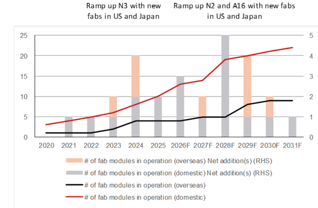
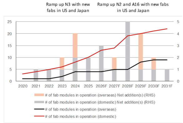
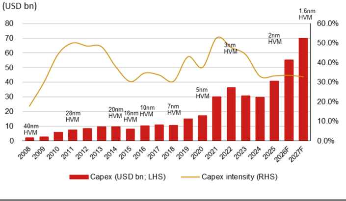
TSMC continues to build up new capacity in Taiwan and overseas. TSMC now has 26 advanced wafer fabs and advanced packaging facilities ramping up or planned globally (18 of them are in Taiwan). We formulate our high-volume manufacturing timeline assumptions in Fig. 18 , which suggests TSMC will have more fab modules coming on stream after 2027F in line with management commentary ‘… So 2026-2027 for the shortterm, we are looking to improve our productivity. 2028 to 2029, yes, we start to increase our capacity significantly’ during the earnings call in early-2026. As a result, we expect TSMC could spend up to around USD70bn of capex in 2027F considering that over 10 new fab modules would be expanded simultaneously in Taiwan and overseas.
Fig. 18: TSMC’s total no. of fab modules and net additions of fab modules
Source: TSMC, Nomura estimates
ve enpoll romeo lapen buulu teaul up tu
80
Fig. 19: TSMC’s capex and capex intensity trend
70
60
50
40
30
20
10
0
We expect TSMC’s capex could reach up to USD70bn in 2027F
HVM
40nm
HVM
Source: Company data, Nomura estimates
2nm
HVM
1.6nm
60.0%
50.0%
HVM
80%
70%
60%
50%
40%
30%
20%
10%
0%
To strengthen local supply chain resilience, enhance the local economy, and reduce carbon emissions during transportation, TSMC has expanded the goal scope for local sourcing globally, encompassing six categories: equipment, components, raw materials, facility systems, automation, and goods across TSMC’s major operational production fabs in the past decade, to aid local suppliers in upgrading technology and quality, cutting costs, and diminishing carbon emissions.
Fig. 20: TSMC’s Semi material, spare parts and back-end equipment localization plan
Source: TSMC, Nomura estimates
Stocks recommended in this Anchor report
Soitec: Leading SOI wafer company in the world
Soitec is the largest SOI wafer supplier globally with around 70% market share (as per our estimates), maintaining its leadership for years (please refer to our 2019 deep-dive report ). However, we believe its growth driver is no longer RF SOI, but photonics SOI, which is likely to be adopted widely in silicon photonic (SiPh)-based photonic integrated circuits (PIC). We think Soitec’s business could return to its 2019-21 glory days. Compared with Bloomberg consensus, we are more bullish on Soitec’s sales contribution from photonics SOI wafers in the coming years. Our sales forecasts for FY27-28F are 38% higher than consensus estimates.
We have a Buy rating and a TP of EUR250 on Soitec. Our TP is based on 8x FY30F P/S with sales of EUR1.12bn, which is in line with its previous peak cycle valuation level in FY21. Risks to our rating and TP include weak optical communication, smartphone, automotive and FD-SOI demand; rising competition from other materials; and oversupply of SOI wafers.
Besi: Leading hybrid bonding tool company
In our advanced packaging sector report published in Feb-25 (‘The evolution of CoWoS, SoIC, and InFO ’), we were conservative on HB demand in 2025. However, we now expect HB demand to surge quickly in 2026-27F on the back of strong demand driven by AI chips, optical communications, and potentially HBMs. Thus, we now believe Besi’s HB orders in 2026-27F could potentially at 70+ and 150+ units. Compared with consensus, we are more bullish on Besi’s HB orders from customers in 2026-27F. Our sales forecast for 2026F is 7% lower, but for 2027F is 8% higher than consensus estimates.
We have a Buy rating on Besi with a TP of EUR340, based on 55x 2027F EPS of EUR6.1. The P/E of 55x is between Besi’s +1 SD P/E to +2 SD of Besi’s P/E range since 2014 as its HB orders will likely reach historical high levels in 2026-27F, in our view. Downside risks: 1) slower-than-expected semi assembly equipment demand and foundry capex raise; 2) slower-than-expected HB adoption; 3) delays in new customers’ project wins and order shipments; and 4) rising competition causing valuation, ASP or gross margin erosion.
GlobalWafers: Third largest Semi wafer company in the world
In addition to regular Semi wafer demand growth and Semi companies’ capex expansion cycles driven by strong AI demand, we see some catalysts driven by the adoption of new Semi technology, including: 1) wafer-bonded NAND; 2) backside power delivery (BPD); and 3) emerging photonics SOI demand, which we believe may drive annual Semi wafer market shipment growth of 10% in 2026-30F. Although, in our view, GlobalWafers’ profitability remains at a low level and Semi wafer prices are unlikely to be revised up meaningfully immediately as existing LTAs have not all been renewed yet, we expect Semi wafer companies’ bargaining power to recover gradually. Compared with consensus, our GPM forecasts for 2026-27F are 1.8-3.8pp lower. Our 2026-28F sales and net profit estimates are TWD61.2-83.5bn and TWD8.2-15.3bn.
We upgrade GlobalWafers to Buy and raise our TP to TWD850 (from TWD480), based on 3.2x 2028F BVPS TWD262 (increased from previously 2.1x 2026F BVPS of TWD230 to factor in the potential upcycle in 2027-28F). Downside risks include: 1) faster-thanexpected entry of China into the 12’ semi wafer market; 2) slower-than-expected market consolidation; 3) worse-than-expected end-demand for the Semi industry; 4) less favorable demand/supply dynamics in the Semi wafer industry; and 5) less-favorable FX volatility and rising material/utility costs.
AEMC: Leading photoresist and photoresist auxiliary supplier in Taiwan
We initiate coverage of Advanced Echem Materials (AEMC) with a Buy rating and a target price of TWD1,500. AEMC is a leading Taiwan-based developer and manufacturer of specialty chemical materials for semiconductor and display applications, and is among the major photoresist (PR) auxiliary domestic suppliers for TSMC. Considering TSMC’s aggressive N3/N2 and sub-2nm capacity expansion plans from 2026-27E onwards and AEMC’s potential market share gain from global peers, we forecast 2026-30F revenue/net income CAGRs of around 30% each for AEMC. Compared with consensus, we are more bullish on AEMC’s long-term business opportunities to further broaden its product portfolio from photoresist auxiliary to photoresist. Our 2026-28F sales and net profit estimates are TWD5.2-8.4bn and
TWD1.4-2.3bn, respectively.
Our TP of TWD1,500 is based on 60x FY28F EPS of TWD25 - the target multiple of 60x reflects our expectation that AEMC would sustainably grow its business with its leading foundry customer and the TAM of PR would expand. Downside risks include: (1) product disqualifications by its leading foundry customer; (2) loss of market share to other competitors; (3) inability to supply more high-end products such as BARC (Bottom Anti-Reflective Coatings) and photoresist.
Ingentec: Leading specialty gas supplier with TGV capability in Taiwan
We initiate coverage of Ingentec, a Taiwanese specialty gas supplier and emerging TGV (Through-Glass Via) glass core substrate manufacturer, with a Buy rating. In our view, Ingentec is positioned at the intersection of two powerful secular trends: 1) the accelerating demand for etch gases driven by memory capacity expansion, particularly 3D NAND; and 2) emerging glass core substrate demand driven by Broadcom from 2027F. We estimate 2026F will be a year of recovery for its core specialty gas business, and its glass core substrate business could emerge from 2027F onwards at the earliest. Thus, we assume there could be more meaningful sales and earnings growth in late 2027F. Compared with consensus, we assume that the glass core substrate business will not contribute meaningful sales and profit until late-2027F with strong sales and profit surge in 2028F (consensus currently estimates strong earnings growth in 2027F already). We also assume Ingentec would need to raise funds by issuing new shares by the end of 2027F to support the rising capex for its glass core substrate business. Our 2026-28F sales and net profit estimates are TWD1.8-9.3bn and TWD46mn-1.2bn, respectively.
Our TP of TWD960 is based on 60x 2028F EPS of TWD16, in the mid-range of the company’s 45-75x P/E over 2021-23, when Ingentec’s specialty gas business was strong, driven by tight supply due to the Ukraine-Russia war. Downside risks include: 1) weaknening semi capex cycle; 2) loss of market share to competitors; 3) delay in the commercialization of next-generation products; and 4) slower-than-expected adoption of glass core substrate.
Kinik: Leading CMP pad conditioner and reclaim wafer supplier in Taiwan
Kinik is the dominant chemical mechanical polishing (CMP) pad conditioner (DBU) supplier to TSMC on advanced nodes, with an ~80% share on the N2 node through a multi-year codevelopment partnership. We believe Kinik’s reclaim/test wafer business (SBU) is also likely to grow along with the recovery of semi wafer demand. Other than these two growth engines, we expect its grinding wheel business (ABU) could be an additional lever if Kinik is able to penetrate into the leading OSAT companies in the long term. Compared with consensus, our GPM forecast for 2026F is slightly higher due to Kinik’s better product mix, and we have also factored in some more grinding wheel business opportunities in 2028F. Our 2026-28F sales and net profit estimates are TWD9.7-14.2bn and TWD2.0-3.0bn, respectively.
We initiate coverage on Kinik with a Buy rating and a TP of TWD840, based on 40x 2028F EPS of TWD21 in the upper half of its historical P/E of 10-45x, to address its stably growing business with its leading foundry customer, as well as the rising TAM across its different business units. Downside risks are: 1) disqualification of products by its leading foundry customer; 2) losing market share to competitors; 3) failure to broaden its product portfolio; and 4) weakening Semi market demand.
Hubei Dinglong: CMP scale-up and photoresist breakthrough
Dinglong’s investment case rests on two reinforcing growth engines: a rapidly scaling CMP consumables franchise and an inflecting photoresist business. CMP pad sales surged 71.2% y-y in 1Q26 to CNY376mn, with monthly shipments exceeding 40k pieces and capacity now at 50k/month, evidencing meaningful share gains at domestic foundries during China’s semiconductor capacity build-out. The CMP slurry segment is also broadening, with recent wins in 12-inch fine slurry, ceria slurry at a leading memory player, and TSV slurry for advanced packaging - collectively unlocking a domestic TAM of over CNY1bn currently dominated by imports. On photoresist, Dinglong has three ArF/KrF products in stable mass supply with several more order conversions expected in 2026E, supported by a completed 300 tons/annum Phase-2 line offering >5x capacity headroom versus current run-rate. With domestic localisation rates still extremely low (~15% for KrF, 2-3% for ArF) and potential export tightening in 2026-27F, the substitution opportunity is substantial - positioning Dinglong as a direct mainland competitor to AEMC’s photoresist ambitions.
We maintain our Buy rating with TP raised to CNY104 (from CNY42), based on 96x
2026F P/E (CNY1.08 EPS), at +2.5x SD of its 5-year historical average P/E of 51x. The target multiple is supported by a 33% earnings CAGR over 2025-28F, with net profit forecast at CNY1,022/1,312/1,675mn for 2026/27/28F. The stock currently trades at 64x 2026F P/E, implying 43% upside to TP. Key catalysts include continued CMP pad share gains at record shipment levels, broadening of the slurry pipeline into import-dominated categories, and accelerated ArF/KrF order conversions as domestic fabs prioritise supplychain localisation. Downside risks include slower-than-expected ArF/KrF ramp-up, customer production delays, and goodwill/integration risk from the lithium materials acquisition.
Anji Microelectronics: Sub-10nm node leader in China and gross margin recovery
Anji is China’s leading CMP slurry supplier, differentiated by its advanced-node positioning and raw-material self-sufficiency. The company is a primary beneficiary of China’s CMP slurry market scaling to an estimated CNY10.5bn by 2028F, with growth concentrated in sub-10nm area. Copper and copper-barrier slurries at a key client have transitioned from qualification to scaled mass production, while 7nm cobalt-interconnect slurry - a greenfield category with no Cabot/DuPont benchmark - is advancing into qualification at a follow-on site. A further incremental driver is one client’s wafer-to-wafer (W2W) hybrid-bonding initiative for 3D DRAM, which increases CMP step count through pre- and post-bonding planarisation. In-house abrasives production supports slurry gross margins of 55-58% (vs. 52-55% at peers), underpinning superior profitability with ROE forecast at 28-30% through 2026-28F.
We maintain our Buy rating with TP raised to CNY360 (from CNY320), based on 42x 2027F P/E (CNY8.52 EPS), at +2x SD of its historical average P/E of 26x. The target multiple is supported by a 25% earnings CAGR over 2025-28F, with net profit forecast at CNY1,097/1,437/1,738mn for 2026/27/28F. The stock currently trades at 34x 2027F P/E, implying 25% upside to TP. Key catalysts include gross margin recovery from 2Q26F as advanced-node mix improves, incremental CMP step pull-ins from the W2W hybridbonding ramp, and continued displacement of imported slurries at sub-10nm nodes. Downside risks include ultra-high-purity silica sol remains Fuso, rising competition from Dinglong in CMP slurries, and potential fab-led vertical integration that could disintermediate third-party suppliers.
=..
3
Can semiconductor materials close the gap with Semi and SPE market growth?
Assembly & Test
Semiconductor materials: ~USD80bn market powered by fab expansion, node migration and advanced packaging
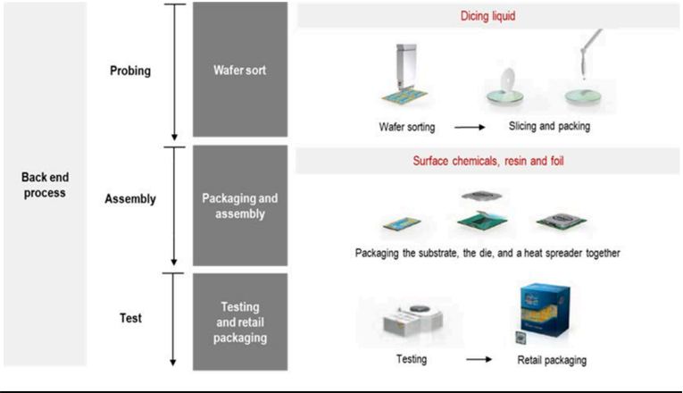
The semiconductor supply chain has been under the spotlight in terms of its importance to international relations, the attention it received from senior leaders in the government and business, and its use as a tool of foreign policy. Across a diverse range of global opportunities and geopolitical challenges, semiconductor materials are increasingly at the center of the story. Semiconductor materials, along with certain chemicals, are necessary inputs across the semiconductor manufacturing process (Fig. 21 ).
Fig. 21: Simplified semiconductor value chain
Source: CSIS, Nomura research
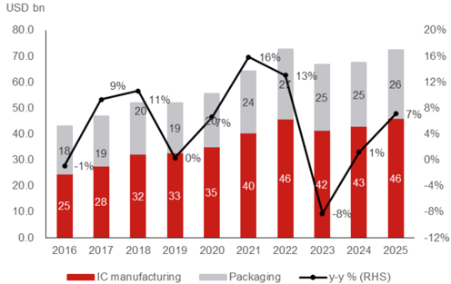
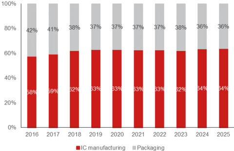
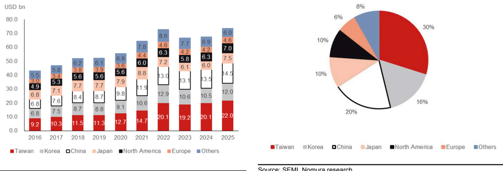
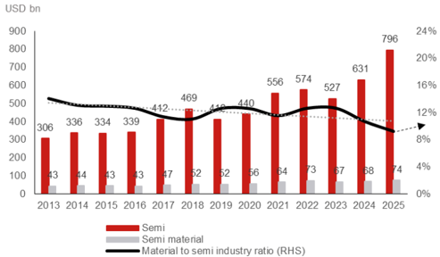
In 2025, global semiconductor sales reached USD796bn (+26% y-y), according to WSTS, while, global total semiconductor material sales merely grew 7% y-y to USD73.6bn. In general, semiconductor materials consist of two main segments - manufacturing materials and encapsulation (packaging) materials (Fig. 22 -23 ). Fabrication materials accounted for 64% of the total material market share in 2025, while packaging materials made up the remaining 36%, as per our estimates.
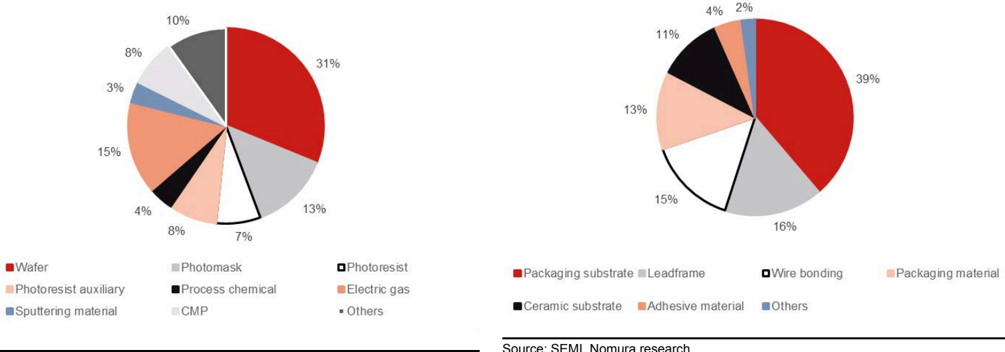
IC manufacturing materials include wafer, photomask, photoresist, photoresist auxiliary materials, process chemicals, electric gas, sputtering material, and CMP materials. According to our estimates, in 2025, wafer represented 31% of total IC manufacturing materials, followed by photo resist and photoresist auxiliary (c.15%), electric gas (c.14%), while photomask and CMP accounted for 13% and 8%, respectively. Packaging materials include packaging substrate, lead frame, ceramic substrate, wire bonding, packaging and adhesive materials, where packaging substrate accounted for the biggest portion of packaging material market with a 39% share, as per our estimates.
somedateu
Sand
Special gas
Seed crystal doping
Slicing liquid
Dicing liquid
Fig. 22: Integrated circuit manufacturing process and corresponding materials
Back end process
Front end
Grinding and polishing slurry
Deionized water cleaning
Source: Nomura research
Fig. 23: Integrated circuit packaging process and corresponding materials
Source: Nomura research
Fig. 24: Semi materials market breakdown by market size
10%
percentage
80.0
70.0
60.0
50.0
40.0
30.0
20.0
10.0
25
0.0
• Wafer
2016
Photoresist auxiliary
•Sputtering material
20%
Fig. 24: Semi materials market breakdown by market size
3%
Source: SEMI, Nomura research
Fig. 26: IC manufacturing materials market breakdown by percentage
11%
Fig. 25: Semi materials market breakdown by percentage
58%
•Packaging substrate # Leadframe
• Ceramic substrate
Source: SEMI. Nomura research
Source: SEMI, Nomura research
Fig. 27: IC packaging materials market breakdown by percentage
Source: SEMI, Nomura research
Source: SEMI, Nomura research
9%
26
12%
18/
Fig. 25: Semi materials market breakdown by percentage percentage
100%
80%
60%
4%
2%
‘you mejor del materiale marnet orare
Fig. 28: Global semiconductor materials sales by market
80.0
70.0
60.0
Fig. 29: Global semiconductor materials sales breakdown, 2025
8%
Taiwan has the highest share in fabrication material consumption, whereas Japan dominates the supply
50.0
40.0
30.0
20.0
10.0
0.0
20%
By country/region, Taiwan remains the biggest semiconductor materials market owing to its large IC foundry and packaging capacities. In 2025, Taiwan accounted for 30% of global semi material sales, followed by 20% for China. South Korea and Japan were the third- and fourth-largest markets, representing 18% and 10%, respectively, of the total share, according to our estimates. The US has been growing rapidly in recent years due to the ‘Made in US’ policy, which is driving more Semi companies to build their new capacities on the US soil.
2016
2017
2020
2021
2018
2019
2022
2023
2024
2025
14%
20%
Fig. 28: Global semiconductor materials sales by market
Photomasks
CMP (slurry and pad)
Other wafer fab materials
9%
34%
Fig. 29: Global semiconductor materials sales breakdown, 2025
11%
Source: SEMI, Nomura research
54%
50%
South Korea
Source: SEMI, Nomura research
•Japan
20%
United States
30%
•Taiwan
• China
Fig. 30: Major semi materials market share of sales by country/region, 2025
Source: SEMI, Nomura research
11%
90%
RoW
5%
100%
7%
12%
40%
12%
13%
30%
8%
12%
16%
16%
Fig. 32: Photoresist - KrF market share by company in 2025
80%
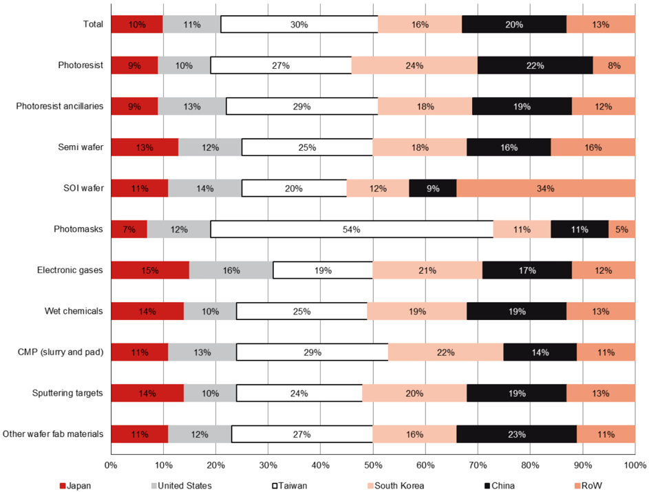
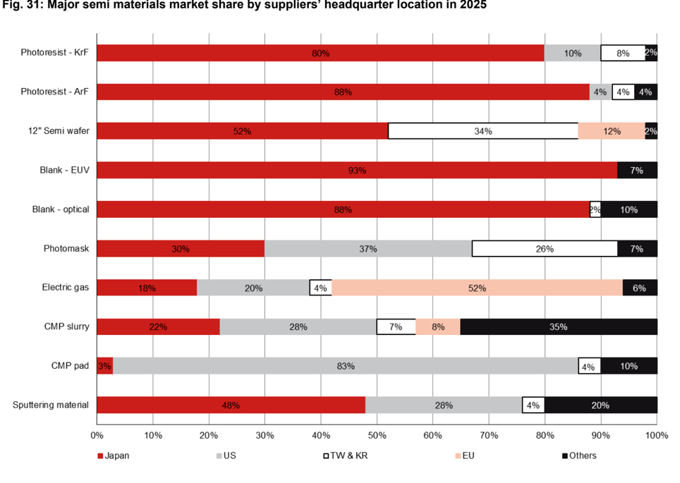
However, the supply of global semi materials is still dominated by Japan, US and EU companies (Fig. 31 -44 ). In details, Japan dominated the lithography and sputteringrelated material market, while the US and EU each have relatively higher shares in CMP and electric gas related markets.
Fig. 31: Major semi materials market share by suppliers’ headquarter location in 2025
Blank - optical
•Fujifilm (JP)
Electric gas
Sputtering material
Fig. 33: Photoresist - ArF market share by company in 2025
10%
8%
4% 4%
12%
2%
4%
2%
Source: Company data, Nomura research
Fig. 32: Photoresist - KrF market share by company in 2025
Fig. 33: Photoresist - ArF market share by company in 2025
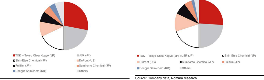
Source: Company data, Nomura research
Source: Company data, Nomura research
Fig. 34: Semi wafer size breakdown by area shipment in 2025
Fig. 36: Photomask market share by company, 2025
Fig. 38: Blanks (optical) market share by company in 2025
10%
Fig. 34: Semi wafer size breakdown by area shipment in 2025
20%
•Captive (TW, US, KR, JP)
•Hoya (JP)
300mm (12”)
•Dai Nippon Printing / DNP (JP)
Shin-Etsu Chemical (JP) |
•LG Innotek (KR)
•Hoya (JP).
- Compugraphics (UK)
Source: SEMI, Nomura research
Fig. 36: Photomask market share by company, 2025
Fig. 35: 300mm water market share by company
Fig. 37: Electric gas market share by company, 2025
Fig. 39: Blanks (EUV) market share by company, 2025
20%
Fig. 35: 300mm wafer market share by company
Source: SK Siltron, Nomura research
Fig. 37: Electric gas market share by company, 2025
Source: Company data, Nomura research
Fig. 38: Blanks (optical) market share by company in 2025
Source: Company data, Nomura research
Fig. 39: Blanks (EUV) market share by company, 2025
Source: Company data, Nomura research
Source: Company data, Nomura research
components in 2025
Fig. 42: CMP pad market share by company in 2025
Fig. 43: CMP pad conditioner market share by company in 2025
Fig. 40: CMP market breakdown by different materials and components in 2025
Fig. 41: CMP slurry market share by company in 2025
•Entegris / CMC Materials (US) • Fujimi (JP)
•Resonac / Showa Denko (JP) Merck KGaA / Versum (DE)
A3M (US)
•Saesol Diamond (KR)
•EHWA Diamond (KR)
• Anji Microelectronics (CN)|
• Shinhan Diamond (KR)
Source: Company data, Nomura research
Fig. 43: CMP pad conditioner market share by company in 2025
Source: Company data, Nomura research
•DuPont (US)
•JX Advanced Metals / JX Nippon (JP)
•Materion / Heraeus (US/DE)
CMP slurry
•JSR Micro (JP)
= Others
•Plansee SE (AT)
• ULVAC (JP)
Source: SEMI, Nomura research
Fig. 42: CMP pad market share by company in 2025
Source: Company data, Nomura research
Fig. 44: Sputtering material market share by company in 2025
Source: Company data, Nomura research
Countries
Taiwan
China
Japan
US
Germany
France
Korea
Companies
Tickers
G-line/t- line
Photoresist
EUV
High-NA
MOR
KrF/ArF
BARC
Photoresist auxiliary
Developer
EBR
Rinse
Fig. 45: Matrix of some key semi materials vs suppliers
Ingentec
Kanto-PPC
B&C Chemical
Air Products
Air Liquide
Saesol Diamond
Precursor Lithograp
Cleaner /Depositi on
MP
MP
hy
UD/MP
Specialty gas
Etching
Doping
MP
MP
Chamber cleaning
MP
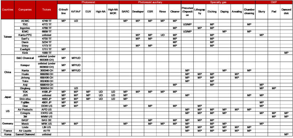
| 4768 TT 6959 TT | MP 333 | MP | |||
|---|---|---|---|---|---|
| 5234 TT 1773 TT 1711 TT | MP | ||||
| 1560 TT | |||||
| unlisted (under | MP MP/UD | ||||
| 603306 CH) unlisted (under | |||||
| 603650 CH) | MP MP/UD | ||||
| MP/UD | |||||
| 300346 CH | MP | ||||
| 688268 CH | |||||
| 688106 CH 002409 CH | |||||
| 688019 CH 300054 CH 4186 JP | MP UD MP | MP | |||
| unlisted | MP MP | MP | 565 | ||
| 4063 J 4901 P | MP MP MP MP | MP | |||
| DOW US | MP MP | ||||
| APD US | |||||
| ENTG US MMM US | 33 | 333 1 33 | |||
| BAS DE | |||||
| MRK US | MP MP | ||||
| LIN US | |||||
| AI FR | |||||
| unlisted |
Source: Company data, Nomura research
Note: MP = mass production; UD = under development
Semi material market growth underperformed Semi and Semi equipment; gradual mean reversion could be seen post 2027F
According to the Semiconductor Industry Association (SIA), SEMI, and Statista, semiconductor materials revenue represented only 9.3% of semiconductor industry market value in 2025, the lowest point since 2013. This implies a USD1bn semiconductor market value would only require USD93mn worth of semiconductor materials (Fig. 46 ). At the same time, the value of SPE has outpaced semi materials since 2017, leading to overall semi material companies’ stock price performances significantly underperforming those of SPE stocks (Fig. 48 -49 ).
The major reasons for the underperformance include:
- The rise of advanced chips such as AI accelerators, which carry significantly high ASPs ·
Since 2023, demand for AI accelerators has surged quickly. Nvidia’s (NVDA US, Not rated) H100/B200 GPUs and custom ASICs from Google (GOOGL US, Not rated) and Amazon (AMZN US, Not rated) command extraordinary price premiums. A single AI GPU can be priced at USD30,000, but the semi wafer and process chemicals inside it cost a few hundred dollars at the most. So, as AI chips boost the total semiconductor revenue figure, materials spending doesn’t keep pace.
- Moore’s Law makes the manufacturing processes more complicated than materials ·
As transistor sizes shrink, more compute cores can be included onto the same physical semi wafer area. As a result, the value of manufacturing processes (more photolithography, etching processes, etc.) extracted per semi wafer has been growing even faster. Thus, revenue per unit of material consumed has continued to rise.
- Semi oversupply cycle has more direct impact on demand for materials ·
Materials consumption tracks fab production and utilization. During downturns, fabs run at reduced capacity, materials purchases fall sharply, but the Semi market doesn’t collapse as dramatically because it includes inventories which can be sold to the market and can charge higher ASPs driven by new applications such as AI and advanced node migrations.
However, we do not rule out the possibility that semi materials market value could see a gradual mean reversal post 2027F, due to:
MP
High-NA
MP
Anealing
Slurry
CMP
Pad
Damond disk
Gate-all-around (GAA) transistors and new materials ·
Moving from FinFET to GAA at 2nm and below requires entirely new material sets nanosheet channels, high-k dielectrics, and new ALD (atomic layer deposition) precursors. Each process step demands higher-purity, more expensive chemicals. The materials cost per wafer at leading-edge nodes is rising faster than at previous transitions.
Backside power delivery and wafer-bonded NAND driving more semi wafer, wafer thinning, grinding and CMP usage ·
Backside power delivery enables power delivery from the first semi wafer’s backside to the active devices in the frontside, with an additional second semi wafer as a permanent carrier. Semi wafer usage and the wafer-thinning process, simply put, will double. Also, CMP usage will increase as well, as both backside and frontside of the first semi wafer are required to be processed.
On the other hand, the wafer-bonded NAND will also drive more semi wafer and CMP usage, in our view, as it involves creating the CMOS circuitry that controls the memory cells and the memory cell array on separate wafers, then inverting the wafer with the memory cell array and bonding the two wafers together.
Photoresist’s value increasing by at least double with the adoption of high-NA EUV ·
Metal-oxide resists are probably the leading alternative to photo acid-driven chemistries, or chemically amplified resists (CAR). These resists offer inherently good etch resistance. The dense core absorbs more energy, too, attenuating electron energy and reducing blur. Due to the change of materials, the photoresist price for high-NA EUV could be much higher than the existing EUV. According to our industry survey, the value of photoresist for high-NA EUV could go as high as USD10,00040,000 per gallon, increasing significantly from USD5,000 for existing EUV.
Advanced packaging adoption rising quickly ·
HBM stacking and chiplet architectures such as AMD’s 3D V-Cache, Intel’s Foveros, TSMC’s CoWoS and SoIC - stack multiple dies together using advanced packaging techniques. This dramatically increases material consumption per final product: more organic substrates, more underfill resins, more copper interconnects, more thermal interface materials.
Glass interposer and glass core substrate are new rising trends ·
Glass core substrates and interposers are being pursued intensively by leading device makers, materials suppliers, and equipment vendors for advanced packaging applications. Taking glass core substrate as example, the cost initially should be higher than existing ABF substrate, considering it is still at an early stage. However, glass core substrate has the following advantages, including: 1) flatness and less warpage; 2) better heat dissipation; 3) low loss favorable to high-speed signaling; and 4) large-format integration; therefore, we expect glass core substrate will play a important role along with existing ABF substrate.
Compound semi and SOI wafers scaling up ·
SiC, GaN, InP and SOI substrates are now widely used for power electronics and optical communication applications and require fundamentally different and more expensive substrate materials than semi wafer.
The avelage glovai sell matchat marnet to sell market late has lanen years
25%
USD bn
900
20%
800
700
600
15%
500
400
300
10%
200
5%
100
0
0%
Source: WSTS, SEMI, Nomura research
24%
USD bn
25
50.0
Fig. 46: Global semi material market to total Semi market ratio The average global semi material market to semi market ratio has fallen below the average level of around 12% since 2024 16%
440
30.0
Source: WSTS, SEMI, Nomura research
Fig. 48: Global SPE market to semi market ratio vs global semi material market to semi market ratio
The content value of Semi materials has underperformed SPE in the past 10 years
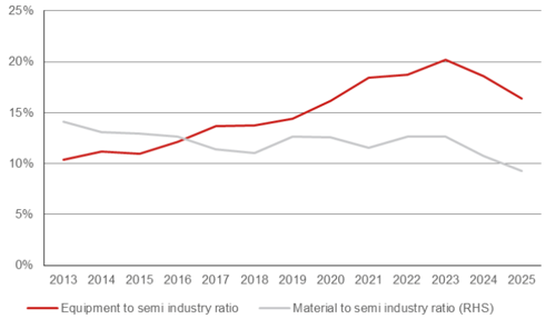
Source: WSTS, Semi.org, Nomura research
12%
306
43
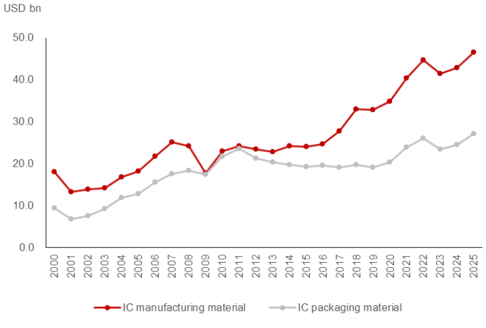
Fig. 47: Semi materials sales: manufacturing vs packaging
Source: WSTS, SEMI, Nomura research
Fig. 49: The performance of global SPE index vs Semi material index vs SOX index since 2013
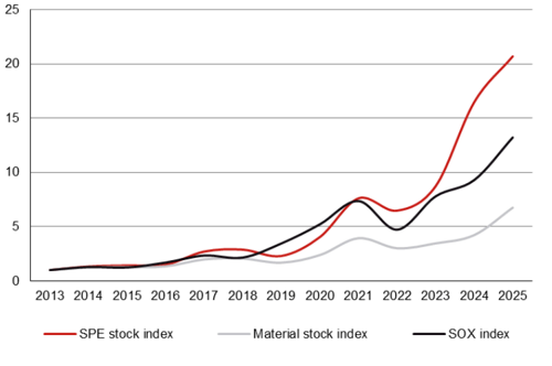
Source: Bloomberg Finance L.P, Nomura research
2025 2030F
CAGR
Fig. 50: Global semi materials sales breakdown by different segment in 2025 vs 2030F
Photoresist
Photoresist auxiliary
Process chemical
Electric gas
Sputtering material
CMP
Others
Packaging substrate
Leadframe
Wire bonding
Packaging material
Ceramic substrate
Adhesive material
Others
| 7.3% | 7.8% | |
|---|---|---|
| 8.0% 7.1% | ||
| 4.1% 3.6% | ||
| 15.3% 13.6% | ||
| 3.4% 3.1% | ||
| 7.7% 8.2% | ||
| 9.9% 8.8% | ||
| Total IC manufacturing material market (USD bn) | 46.5 85.0 | 12.8% |
| 38.7% 49.9% | ||
| 16.2% 12.2% | ||
| 12.9% 12.1% | ||
| 10.7% 7.7% | ||
| 4.4% 4.5% | ||
| 2.2% 2.5% | ||
| Total IC packaging material market (USD bn) | 27.1 45.1 | 10.7% |
| Total Semi material market (USD bn) | 73.6 130.1 | 12.1% |
Source: SEMI, Nomura estimates
The evolution of TSMC’s local sourcing plan
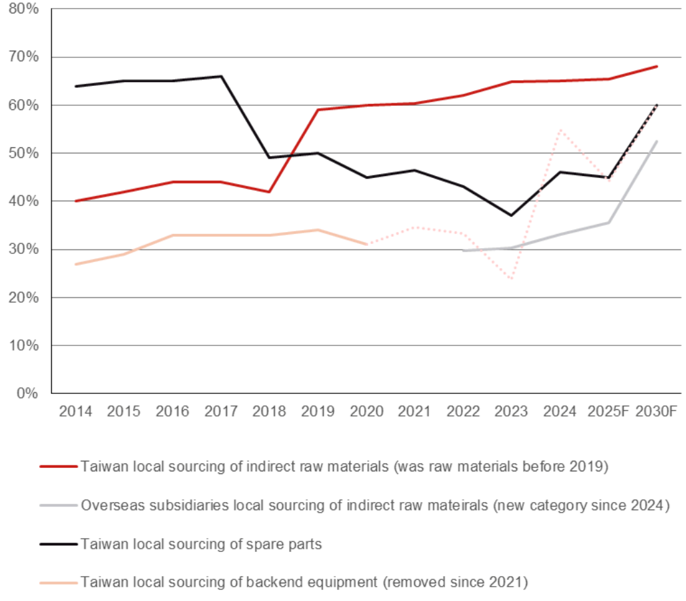
To strengthen local supply chain resilience, enhance the local economy, and reduce carbon emissions during transportation, TSMC has expanded the goal scope for local sourcing globally, encompassing six categories: equipment, components, raw materials, facility systems, automation, and goods across TSMC’s major operational production fabs (TSMC fabs in Taiwan, TSMC (China), TSMC (Nanjing), TSMC Washington, LLC, TSMC Arizona, and JASM) over the past decade, to aid local suppliers in upgrading technology and quality, cutting costs, and diminishing carbon emissions. Concurrently, localized procurement objectives have been defined at each site to reinforce global capabilities for regional material supply.
The goal has been changed a few times since 2018, including:
- As the production capacity of silicon wafers (semi wafer) in Taiwan failed to meet TSMC requirements, the target of local sourcing was adjusted from “local sourcing of raw materials” to “local sourcing of indirect raw materials” in 2018. 1.
- For backend equipment, since the proportion of advanced packaging has increased and both quality requirements and technical specifications have become stricter, TSMC has also increased the procurement volume of domestic and foreign suppliers, and the demand for foreign suppliers is still strong; therefore, TSMC removed the target beginning in 2021. 2.
- In 2020-23, the proportion of spare parts in advanced processes increased compared to previous years. However, the localization of spare parts in advanced processes is still in the development stage, so the annual target was not reached. 3.
- To improve transparency in localized procurement information, a new management indicator for the local procurement ratio of overseas subsidiaries was introduced in 2024. 4.
Based on these changes, we summarize the read-across to TSMC’s suppliers by different sectors:
- TSMC has high specs for semi wafer, which is the largest portion of the semi raw materials market. As TSMC has still not yet brought back its target of ‘local sourcing of raw materials’, we believe the leading semi wafer companies in Taiwan, such as GlobalWafers, may still have room to strengthen its technology capability to meet TSMC’s requirements, particularly for advanced node production. 1.
- For indirect raw materials, we believe the future growth driver is likely to be TSMC’s overseas facilities, particularly TSMC Arizona, which is likely to become an important facility that will ramp up products continuously, while the localization rate in Taiwan has been increasing to a relatively high level. 2.
- TSMC indicated that the spare parts and back-end equipment localization rates were not satisfactory due to the rising requirements for advanced processes and packaging, which implies there may be still room for spare parts and back-end equipment companies to further strengthen their technology capabilities. 3.
80%
70%
60%
50%
40%
30%
20%
10%
0%
fabs in US and Japan
Ramp up N2 and A16 with new fabs in US and Japan
Fig. 51: TSMC’s semi material, spare parts and back-end equipment localization plan
20
15
10
5
0
Source: TSMC, Nomura estimates
TSMC’s capex in 2027F could exceed market expectations
TSMC continues to build up new capacity in Taiwan and overseas. TSMC now has 26 advanced wafer fabs and advanced packaging facilities ramping up or planned globally (18 of them are in Taiwan). We formulate our high-volume manufacturing timeline assumptions in Fig. 52 -53 , which suggest that TSMC will have more fab modules coming onstream in post 2027 and are consistent with management commentary: ‘… So 2026-2027 for the short term, we are looking to improve our productivity. 2028 to 2029, yes, we start to increase our capacity significantly’ during the company’s earnings call in early-2026. As a result, we expect TSMC to spend up to around USD70bn in capex in 2027F considering more than 10 new fab modules would be expanded simultaneously in Taiwan and overseas.
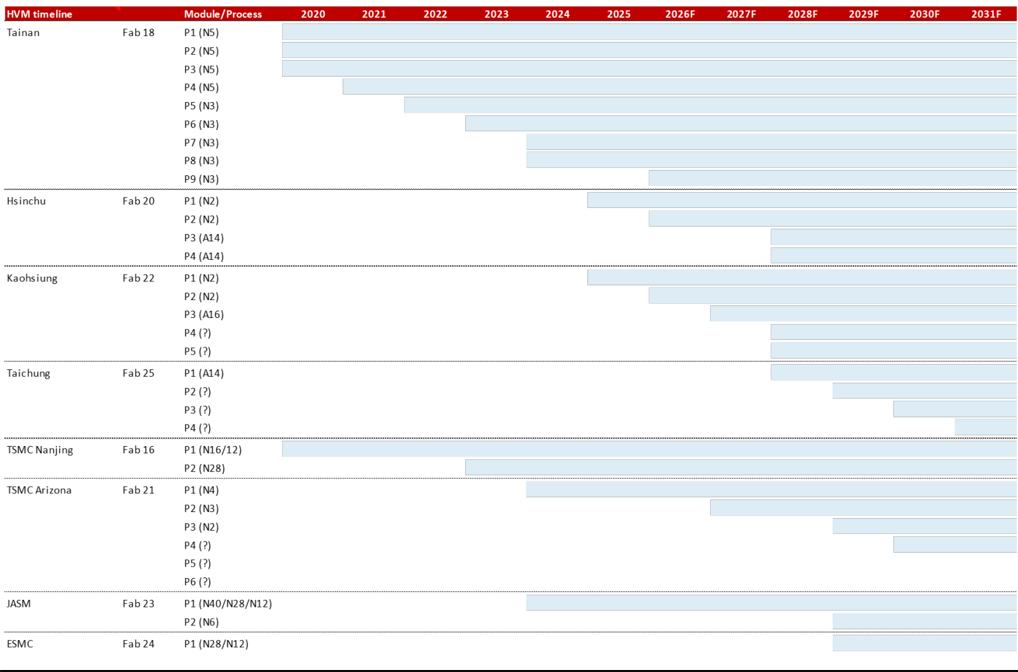
Fig. 52: TSMC’s total fab module numbers and the net additions of fab modules
Source: TSMC, Nomura estimates
4
Tainan
80
70
60
50
40
Hsinchu
30
20
10
40nm
HVM
Kaohsiung
0
Taichung
TSMC Nanjing
TSMC Arizona
JASM
ESMC
2020
2021
P2 (N5)
Fig. 53: TSMC’s fab expansion plans
2026F
60.0%
| P5 (N3) | ||
|---|---|---|
| P6 (N3) | ||
| P2 (N2) | ||
| Fab 16 | P2 (N28) | P1 (N16/12) |
| Fab 21 | P1 (N4) | |
| P4 (?) | ||
| Fab 23 Fab 24 | P1 (N40/N28/N12) P2 (N6) | P1 (N28/N12) |
Source: TSMC, Nomura estimates
Fig. 54: TSMC’s capex and capex-intensity trends
We expect TSMC’s capex could reach USD70bn in 2027F
Source: Company data, Nomura estimates
2022
2023
2024
2nm
2025
1.6nm
HVM
2027F
2028F
2029F
2030F
DUV
ArFi
NXT1980
Model year
2015
2016
Wave length
193nml
193nm
WPH
250
275
Numerical aperture
1.35
1.35
Mix-and-match overlay
Resolution (half pitch)
3.5nm
2.5nm
High-NA EUV - the evolution of EUV in A10 node onward 13.5nm 160 0.33 1.1nm
Currently, the most advanced chips are manufactured using EUV lithography, specifically ASML’s Twinscan NXE:3400C system, which has 0.33 numerical aperture (NA) optics, providing a 13nm resolution (half pitch). This level of resolution is sufficient for a singlepattern approach at 7nm/6nm nodes, with around 36nm metal pitches (>13nm*2=26nm), and at 5nm with around 28nm metal pitches. However, as the metal pitches decrease below 26nm (beyond the 3nm node), 13nm resolution might require double patterning. For post-3nm nodes, ASML and its partners are developing a new EUV tool called the Twinscan EXE:5000-series with a 0.55 NA (High-NA) lens that can achieve 8nm resolution, which is anticipated to eliminate multi-patterning at 3nm and beyond. Intel had already installed high-NA EUV in 2H24 for its 14A node development, and TSMC in 2025F for its 2nd-gen 1.4nm development. Although High-NA scanners are still under development and the usage for major customers’ mass production may not happen until 2029-30F (as TSMC would not use high-NA for mass production until A10), we believe high-NA EUV is expected to be extremely complex, large, and expensive, with a price tag of over USD400mn each. Additionally, these scanners will require new optics, a new light source, and even new fab buildings to accommodate them. Despite these challenges, leading makers of logic chips and memory devices are willing to adopt new technologies to keep up with the scaling of performance, power, area, and costs (PPAc) of semiconductors. Therefore, high-NA EUV scanners are crucial, in our view.
Fig. 55: Specs of ASML’s DUV and EUV
Source: ASML, Nomura research
The three factors of photolithography - wave length, numerical apertures, and k1 coefficient
The critical dimension (CD), the smallest possible feature size that can be printed with a certain photolithography-exposure tool, is proportional to the wavelength of light divided by the numerical aperture (NA) of the optics. So, smaller CDs can be achieved by using either shorter light wavelengths or larger numerical apertures, or a combination of the two. The k1 value can be pushed as close as possible to its physical lower limit of 0.25 by improving manufacturing-process control. The formula is ‘CD=k1*(wave length/NA)‘.
In general, the most economical ways to boost resolution are by increasing the numerical aperture and by improving tool and process control to allow for a smaller k1. Only after chipmakers run out of options to further improve NA and k1 do they resort to reducing the wavelength of the light source. The switch to EUV (13.5nm light) from 193nm light has done part of the job of decreasing CD. Now it looks like NA will be boosted again, from today’s 0.33 to 0.55.
How high-NA EUV works? Anamorphic optics is critical
Increasing the NA from 0.33 to the target value of 0.55 inevitably entails a cascade of other adjustments. Projection systems such as EUV lithography have an NA at the wafer and also at the mask. When you increase the NA at the wafer, it also increases the NA at the mask. Consequently, at the mask, the incoming and outgoing cones of light become larger and must be angled away from each other to avoid overlapping. Overlapping cones of light produce an asymmetric diffraction pattern, resulting in unpleasant imaging effects.
⇐38nm
⇐38nm
⇐38nm
⇐38nm
⇐13nm
⇐13nm
⇐13nm
⇐13nm
⇐13nm
⇐8nm
14-28nm
7-14nm
7nm
5-7nm
5-7 nm
5-7 nm
3-5nm
1.4-3nm
1.4-3nm
1-2nm
1-2nm
The reflection decreases significantly when angle
ML reflection field printing as well
0.33 NA
0.55 NA
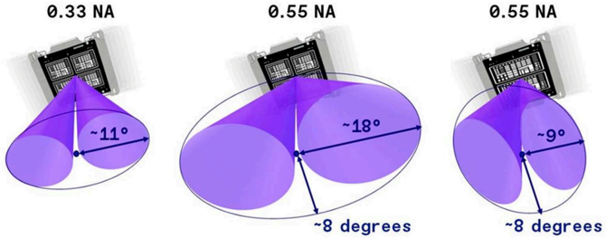
But there’s a limit to this angle. Because the reflective masks needed for EUV lithography are actually made of multiple layers of material, it is not possible to get a proper reflection above a certain reflective angle. EUV masks have a maximum reflective angle of 11 degrees. There are other challenges as well, but reflective angle is the biggest, according to ASML. ~11°
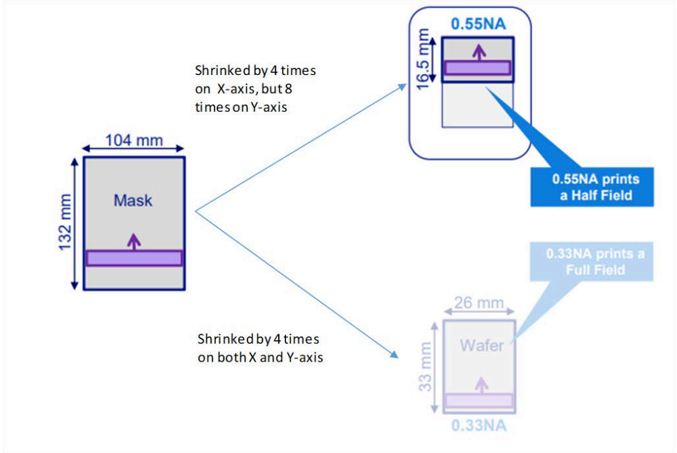
The angle of reflection at the mask in today’s EUV is at its limit of 11 degrees. Increasing the NA of EUV would result in an angle of reflection that is too wide (more than 15 degrees). So high-NA EUV uses anamorphic optics supplied by Zeiss (unlisted), which allow the angle to increase in only one direction on the X-axis. The field that can be imaged this way is half the size on the Y-axis, so the pattern on the mask must be distorted in one direction, but that’s good enough to maintain throughput through the machine. Shrinked by 4 times on both X and Y-axis
0.55NA
,26 mm,
Wafer
Fig. 57: EUV: High-NA requires an anamorphic lens
The anamorphic lens can reduce the angle of incidence on the Y-axis by half, but results in a halffield printing as well
Source: ASML, Nomura research
Fig. 59: Half-field printed chips vs full-field printed chips - 2
Source: ASML, Nomura research
0.7
0.6
0.5
0.4
0.3
0.2
0.1
0
Fig. 56: Mask multilayer reflection vs angle of incidence
The reflection decreases significantly when angle of incidence is approaching 15 degrees
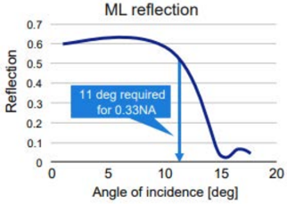
Source: ASML, Nomura research
Fig. 58: Half-field printed chips vs fullfield printed chips - 1
The size of half field printed chip is half of full field’s
Source: ASML, Nomura research
0.55 NA
~9°
0.55NA prints a Half Field
0.33NA prints a
Full Field
~8 degrees
0.33 NA EUV
0.55 NA EUV
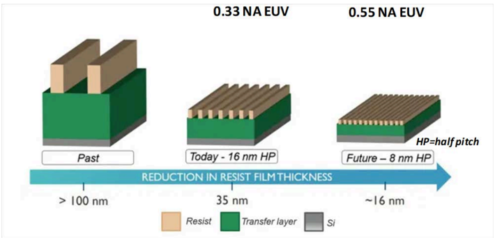
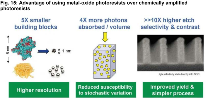
Photoresist, stitch overlay control, SoIC (hybrid bonding), and absorber for mask are also critical for high-NA EUV
Based on the fundamentals of high-NA EUV and the difficulties found during the R&D stages, we expect there are two critical technology issues that need to be resolved: photoresist and stitch overlay.
The change of photoresist and related materials are required
HP=half pitch
With a higher NA, photons strike the wafer at a more shallow angle. That requires thinner photoresist layers are needed to avoid shadowing. The upside is that a thinner resist layer reduces the risk of pattern collapse, as the aspect ratio of resist features is smaller. However, it also provides less protection for the wafer. In addition, long etch processes used to create high-aspect-ratio wafer features can erode the resist layer, ultimately degrading the transferred pattern. With less material, a thinner resist also captures fewer photons, potentially making roughness and other stochastic effects worse.
At present, metal-oxide resists are probably the leading alternative to photo acid-driven chemistries, or chemically amplified resists (CAR). Based on a metal-oxide core, surrounded by ligands that tune solubility, cross-linking, and other properties, these resists offer inherently good etch resistance. The dense core absorbs more energy, too, attenuating electron energy and reducing blur. Due to the change of materials, the photoresist price for high-NA EUV could be much higher than for the existing EUV. According to our industry survey, the value of photoresist for high-NA EUV can go up to USD10,000-40,000 per gallon, a significant increase from USD5,000 for existing EUV.
Improved etch resistance and absorption address the most serious limitations of thin resists, offering a high NA-friendly solution. Unfortunately, only negative tone metal-oxide resists are available, so they cannot be used for contact holes. Both Inpria (acquired by JSR) and Lam Research offer metal-oxide resists, differentiated in part by their approaches to development.
Lam Research is attempting to disrupt the whole stack. Instead of a wet PR technology using a spin coater, it plans to use a chemical vapor deposition process to layer on a metal PR. The throughput and patterned lines would be slower but more accurate. If using Tokyo Electron (TEL) (8035 JP, Buy) and JSR’s solution, due to the change of the PR materials, the developer would need to be changed as well. Currently,
Tetramethylammonium Hydroxide (TMAH) is widely used as developer for existing EUV. But for high-NA EUV, propylene glycol methyl ether acetate (PGMEA) with acid is likely a better solution. We expect TOK is likely the major supplier. The purity requirement of developer would be higher as well.
Although the existing wet process solution supplied by TEL and JSR will be likely more cost effective without procuring the new equipment, we expect TSMC could be more likely to adopt Lam Research’s solution in the high-NA EUV era.
Fig. 60: Reduction in photoresist film thickness
Source: Cadence, Nomura research
Lall nesear ulle bolly uly depostun allu uly uevelop eyurpment lu growemmale photoreolol
Mithough Mon cales Wighel nor, the uodge lo much smallel that legulal mighta suv photoresist
4X more photons absorbed / volume
building blocks
45000
40000
>>10X higher etch selectivity & contrast
Fig. 61: Advantage of using metal-oxide photoresists over chemically amplified photoresists
Wet photoresistapplication - adding up photoresist
35000
30000
25000
Exposure - EUV
20000
15000
Higher resolution
Wet developing - washing out the photoresist by using solvant
10000
5000
Etching
0
High-NA MOR
Source: Inperia, Nomura research
Fig. 62: Price of photoresist per gallon
Although MOR carries higher ASP, the usage is much smaller than regular high-NA EUV photoresist
Source: Nomura estimates
Fig. 63: TEL and JSR vs Lam Research’s solution
Lam Research is using dry deposition and dry develop equipment to grow/eliminate photoresist
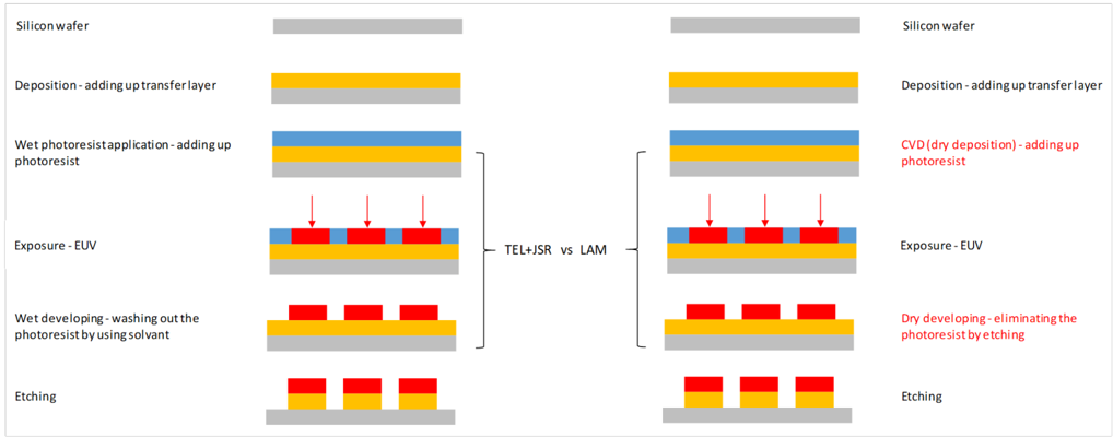
Source: TEL, Lam Research, Nomura research
High-NA
LoW-NA
Silicon wafer
Deposition - adding up transfer layer
CVD (dry deposition) - adding up photoresist
Exposure - EUV
Dry developing- eliminating the photoresist by etching
Etching
ASP (USD per gallon)
Nodes (nm)
Suppliers
Note
‹100
100-1000
ArF
1000-1500
EUV
1000-5000
High-NA EUV
5000
Fig. 64: Specs of different photoresists by nodes and major suppliers
High-NA MOR (metal oxide resist)
10000
>40000 (but with low throughput)
13.5 (with 0.55 NA)
⇐1nm
| TOK | Shin-etsu | Shin-ets u | Shin-etsu TOK | Entegris | Entegris |
|---|---|---|---|---|---|
| Dow | JSR | TOK | JSR Shin-etsu | Gelest (Nanomate) | |
| Merck | Dow | Sumitomo | |||
| Fujifilm | Fujifilm | ||||
| TOK is the | TOK is the | ||||
| Market share consolidation to winner of EUV | Market share consolidation to winner of EUV | JSR could regain share in high-NA EUV technology could outpace Tokyo Electronc’s track technoloy | |||
| photoresist | photoresist | 2. Entegris and Gelest (through | |||
| market used ony 1-2nm nodes | market used ony 1-2nm nodes | Nanomate in Taiwan) could be the | |||
| new photo resist suppliers |
Source: Nomura estimates
Stitch overlay control for large-die-size ICs is critical, in our view
ICs with very large die sizes have become important products for the semi industry, such as Nvidia’s gaming and AI GPUs and certain high-performance computing chips from Intel, Google and Tesla. These processors are so large that only one die can fit in a 26mm33mm exposure field, and such devices are too large to fit in the half-field (only 26mm16.5mm) of high-NA exposure tools. In order to continue producing devices with similar chip sizes when entering into sub-2nm nodes, stitching will need to be adopted. With stitching, part of the chip layout is patterned using one mask, while the remainder is patterned by exposure to a second mask.
Stitching requires very precise implementation by the tight process control requirements of the nodes at which high-NA EUV lithography will be applied. There are also special considerations that apply to EUV lithography. In addition to pattern-placement errors, there could be aerial image cross-talk across the stitch boundary, as well as variations in flare due to different pattern densities on the two sides of the boundary. These phenomena that affect critical dimensions can be compensated through OPC, and pattern placement errors can also be corrected by calculating the displacement due to stress reduction and compensating during mask writing. Because the magnitude of these effects is the greatest near the stitch boundary, and the accuracy of such corrections may become inadequate very close to the boundary, a 1μm exclusion zone between subfields has been proposed. While such an exclusion zone would have little impact on the number of dies per wafer, it does preclude geometries that cross-stitch boundaries, such as interconnects. Fortunately, the tightest pitch metal layers are usually confined to logic and memory cells and local routing. These can be done with high-NA EUV lithography, while the routing that needs to cross-stitch boundaries can be patterned using 0.33 NA EUV lithography. It is also reasonably straightforward to avoid having contacts and vias within this exclusion zone. The special issues associated with stitching provide additional motivation for using multiple patterning with 0.33 NA exposure tools rather than high-NA EUV lithography, particularly for across-die routing.
JSR
JSR
vesign, thus the siligle ale size lo 10l as big do those of to peels.
Sapphire or odd dies distributed across two masks
Similar to field-to-field interactions for NXE
Emerald
Fig. 65: High-NA EUV process for large and small die size ICs
Die ≤ High NA field
3 rows
The stitching (two reticles exposure) will only be seen on the ICs with die size larger than 16.5mm*26mm
5 rows
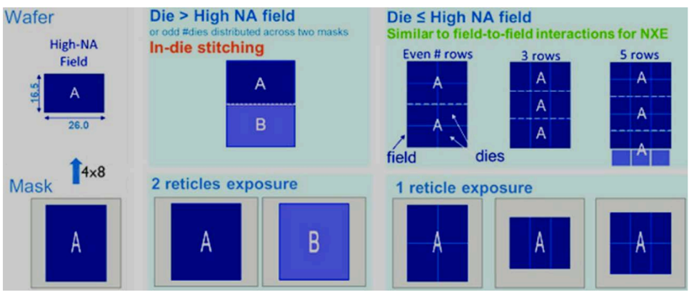
XCC
678
TU102
754
Mask
TPUV2
625
M2 Max
~500?
Tesla
D1 chip
645
Source: SPIE, Nomura research
Fig. 66: Some leading semi companies have large die size chips over 429mm^2 (half field)
Die size larger than 429mm^2 are mostly used for servers, AI, and gaming. AMD has turned to chiplet design; thus the single die size is not as big as those of its peers.
Source: Company data, Nomura research
The material of absorber on mask could be changed to enhance contrast and reduce dosage
Tantalum-based absorbers for EUV masks enabled the development of EUV lithography. However, with dimensions shrinking, mask 3D effects are becoming increasingly significant when such absorbers are used. Recent efforts have gone into identifying new mask absorbers for both binary and attenuated phase-shifting masks (attPSM). For binary masks, mask 3D effects can be reduced by having the real part of the index of refraction of the absorber be close to 1.0, while the extinction coefficient (k = imaginary part of the index of refraction) should be as large as possible. This latter condition enables the use of thin absorbers.
Since it is desirable to have an appreciable amount of reflection from the absorber on an
Extinction coefficient k attPSM, the absorber should have a moderate extinction coefficient. This means that candidate elements for the absorbers of attPSMs should be those in the lower left corner of Fig. 67 , although they may be alloyed with other elements. Since rhodium (Rh) is an extremely rare element, all isotopes of technetium (Tc) are radioactive, and there is a dearth of volatile compounds of palladium (Pd), absorbers for attenuated phase-shifting masks need to contain substantial amounts of ruthenium (Ru) or molybdenum (Mo). This has implications for the capping layer, which has long been composed of ruthenium, since the capping layer has also provided etch selectivity to the absorber. Accordingly, use of absorbers containing a significant amount of ruthenium will also require an alternative capping layer.
However, this change may not bring huge value addition to mask makers, in our view, as there are already Ru and Mo-based materials in a mask, so it is mainly the change of material mix by using more Ru and Mo-based materials to replace the existing TaBN materials. The price of the mask is mainly decided by the blank defect quality - if the mask has no defect, it can be extremely expensive. Since it has been already the case for EUV masks, the incremental value added to mask makers from the change of the materials of absorber is limited, in our view.
Fig. 67: Refraction index n vs extinction coefficient k by different materials
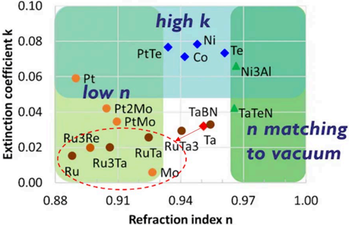
Source: IMEC, Nomura research
It could be changed from TaBN
to low n materials such as Ru
Capping layer
Multilayer for EUV
reflection
Substrate
Back-side film
Source: Hoya, Nomura research amplified, with better intensity at wafer and result in clearer IC circuit
(a) Conventional
Amplitude of light
at mask
Amplitude of light
at wafer
Intensity at wafer
Source: Research Gate, Nomura research
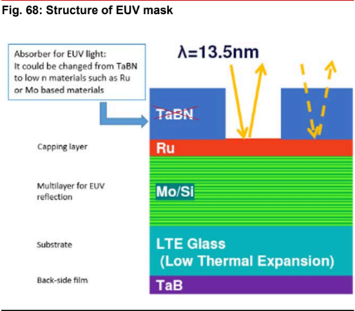
Source: Hoya, Nomura research
(b) Attenuated
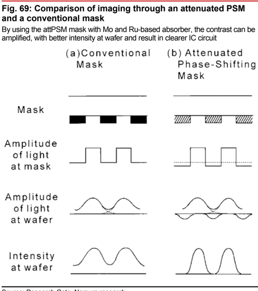
Л=13.5nm
lle vollel vowel bulloutiytlul
Te lalgel cumaul ar eas,
3D transistors and SoIC are playing more important roles
3D transistors rising as pitch scalability is slowing down
A major feature of logic ICs is the 3D circuit. In recent years, this trend towards 3D has gradually moved away from overall circuit design towards the internal structure of the transistor. As circuits shrink, the contact plane between the gate and the electronic channel below also shrinks, making it less able to control current. In the 1990s, Professor Chenming Calvin Hu and his team invented the ‘fin field-effect transistor’ (FinFET). The electronic channel of the FinFET is a fin-like plate structure that wraps into the gate, thus increasing the contact surface from one side to three sides, a significant design improvement. The next goal is to build a ‘gate-all-around field-effect transistor’ (GAAFET), in which the gate material surrounds the channel region on all sides (four sides).
Fig. 70: Contact area between gate and source/drain electrodes
The larger contact areas, the better power consumption

Source: Samsung, Nomura research
Moore’s Law may still continue along with the pitch to scale down further once the leading semi companies start to adopt high-NA EUV at around 1nm (A10). In this case, the giants in the semi market, such as ASML and TSMC, could still widen their technology leadership over other semi companies for next decade. However, if high-NA EUV eventually proven to be less cost effective, the pitch scaling could be no longer the key topic in the future, where the whole Semi industry will focus more on device/transistor structure innovation, from 2D to 3D structure with more complicated, and transistors are stacked on top of each other, called a complimentary FET (cFET) device.
GAAFET
(Nanowire, Nanosheet, Forksheet)
70
60
50
Metal Pitch
(am)
40
Metal Tracks
30
FinFET
N16 N10
Potential roadmap extension
Fig. 71: Metal pitch scaling trend in the history
40
2032
2034
A5
A3
2036
A2
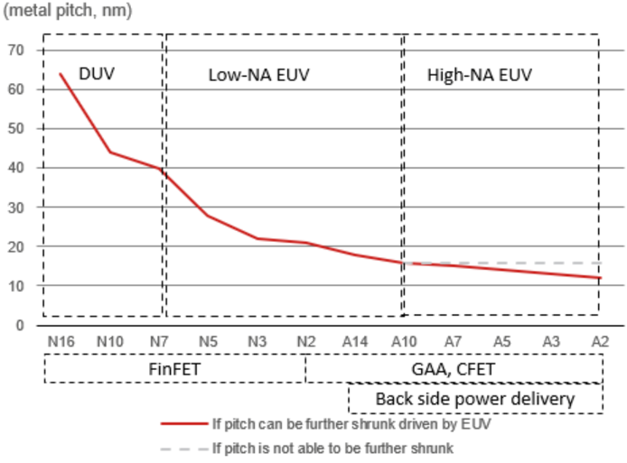
Source: Nomura estimates, IMEC
Fig. 72: Semi logic nodes roadmap
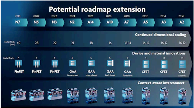
Source: IMEC, Nomura research
We are reminded of the lessons learned from the NAND industry. In 2017, when the semi industry witnessed a migration of 2D NAND to 3D NAND, there were two consequences:
Etching and CVD-related process demand surged more than the industry average level 1.
In 2016-17, the NAND industry started to migrate NAND manufacturing technology from 2D NAND to 3D NAND, which drove strong equipment demand for etching and CVD (including ALD and LPCVD) processes. Thus, we expect once the transistor structure of logic IC also migrates from 2D to 3D, demand for those types of equipment will also surge strongly.
The approach to fabricate stacked-Si nanowires for GAA devices in Fig. 74 includes: 1) a stack of Si/SiGe layers are grown on silicon wafer; 2) anisotropic plasma etching (vertical direction) is achieved in an inductively coupled plasma (ICP) reactor; 3) there is isotropic and selective etching (both vertical and horizontal directions) of SiGe
High-NA EUV
20
10
0
25
20
15
101
Si 10 mm
Si 10 nm
Isotropic etching in RPS reactor: cycle of a two-step process
Over 20% was a danger zone during the semicon bubble
(USD mn)
- 180,000
Llle
In ICP reactor
Oxidation
Etch
Oxidation
Etch layers in an RPS (remote plasma source) reactor; 4) a two-step process alternates oxidation (ALD) and etch; 5) horizontal Si nanowires are released.
nanowires
Al demand to drive advanced node, advanced
The key players of etching and CVD equipments worldwide include LAM Research, Applied Materials, TEL, and ASM International. 120,000
It could be easier for new entrants, such as YMTC, to catch up with market leaders if pitch scaling slows down 2.
93
packaging and memory capacity expansion to
100,000
further accelerate
→
SiO, BOX 20 nm
Si substrate
80,000
However, if the pitch scaling of logic IC is halted or slows down meaningfully, new entrants or lower-tier players could catch up more easily with the market leaders, which used to be able to widen the technology leadership by pushing the pitch smaller, as the technology barrier of pitch shrink is higher than the structure change from 2D to 3D. For example, YMTC (unlisted), as a new entrant to the NAND industry since 2019, could quickly ramp up its production capacity with technology improvement from 32-layer 3D NAND to 128-layer 3D NAND within just four years. 40,000
As a result, although currently high-NA EUV is still in the R&D stage with many technology difficulties yet to be resolved, our basic assumption is that semi giants such as ASML and TSMC would want to make it happen, as they could lose their leading positions in a brutal semi market where only market leaders are able to enjoy excess profits.
Fig. 73: Global SPE market to semi market ratio
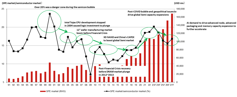
Source: Nomura estimates based on Gartner, WSTS and SEMI data
Source: Journal of Vacuum Science & Technology A Vacuum Surfaces and Films, Nomura research
Si substrate
91 92
Fig. 78: Etching equipment market share, 2025
segments
50,000
40,000
30,000
20,000
10,000
Lithography/Resist
•Lam Research
Epitaxial system
Batch atomic layer deposition (ALD)
Plating equipment
Channel hole etching
Forming charge trap segments
Fig. 79: CVD equipment market share, 2025
30.0%
CMP
Flattening of broad aren
25.0%
Fig. 75: Key processes and main production equipment for 3D NAND
15.0%
Source: Nomura research
Fig. 76: Global SPE market by different front-end equipment segments
Source: Gartner, Nomura research
Fig. 78: Etching equipment market share, 2025
Etching systems
Fig. 77: Global SPE market % by different front-end equipment segments
Source: Gartner, Nomura research
Fig. 79: CVD equipment market share, 2025
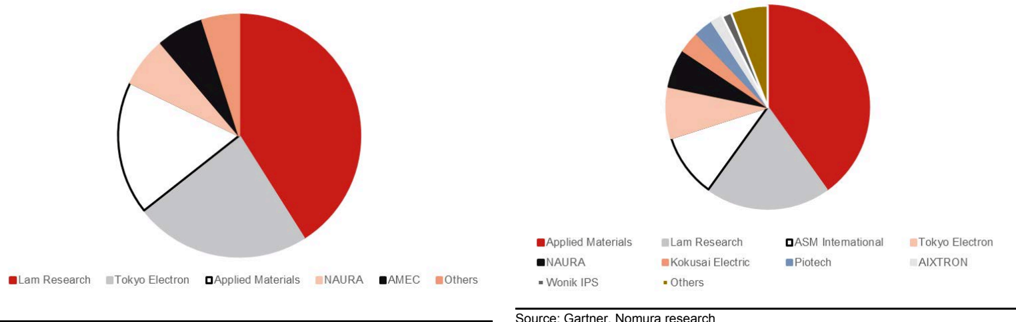
Source: Gartner, Nomura research
Source: Gartner, Nomura research
Etching systems
Channel hole formation
Fig. 80: TSMC’s potential monthly SolC capacity
(kwpm)
Fig. 81: Besi’s hybrid bonder order
(units)
SoIC (hybrid bonding) demand to surge quickly in 2026-27F on wards; TSMC’s SoIC capacity will likely grow significantly
2024
An alternative solution to the high-NA EUV stitching issue is the avoidance of large dies altogether. With advanced packaging, it has proven possible to maintain high performance even while separately fabricating parts of circuits that previously had been fully integrated into a single die. This is currently being done to improve the costeffectiveness of advanced lithography. For example, the high-performance logic circuits of AMD’s EPYC processor have been fabricated using 7nm technology, while input/output functions have been fabricated using lower-cost 14nm processes. In other applications, memory access rates have been improved using advanced packaging technology. It may also be possible to achieve high levels of performance with maximum die sizes that can fit into the exposure fields of high-NA EUV exposure tools.
SoIC demand was slow across the industry in 2025, mainly due to:
-
- Intel held up the capex;
-
- TSMC’s SoIC demand not growing as there was no meaningful new customers other than AMD and Apple (AAPL US, Not rated) yet;
-
- AMD’s AI chip demand was not as strong as expected.
However, we expect the SoIC demand to surge quickly in 2026-27F mainly as:
-
- AMD’s SoIC demand is re-accelerating;
-
- We expect COUPE (EIC and PIC stacking) will start to use hybrid bonding technology from 2026F onwards;
-
- Samsung (005930 KS, Buy) and Hynix (000660 KS, Buy) are procuring some hybrid bonding equipment for small volume of HBM stacking production;
-
- Intel resumes some equipment procurement
Based on our estimates, TSMC’s SoIC capacity was around 1.9k pieces by the end of 2023F, and it likely expanded to over 4k by the end of 2024F, as AMD MI300 widely adopted SoIC with growing volume throughout 2024. SoIC capacity could have further expanded to ~10k or higher by end-2025F, and is likely to accelerate to 15k/30k in 2026F/2027F to match future demand growth. As a result, we estimate TSMC’s SoIC capacity will record a CAGR of over 90% in 2025-27F, which will also drive a significant recovery in hybrid bonder orders in 2026-27F from 2025 trough levels.
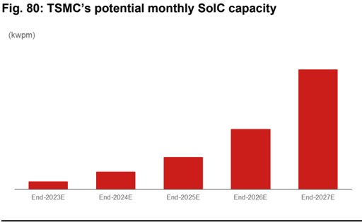
Source: Nomura estimates
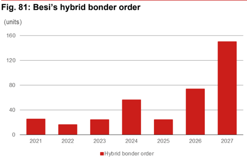
Source: Company data, Nomura estimates
2025
2026
2027
enrical
Fig. 82: Hybrid bonder order breakdown by different end applications/customers in units, 2026F Chip 2
& SiO, to
Chip?
Chip 4
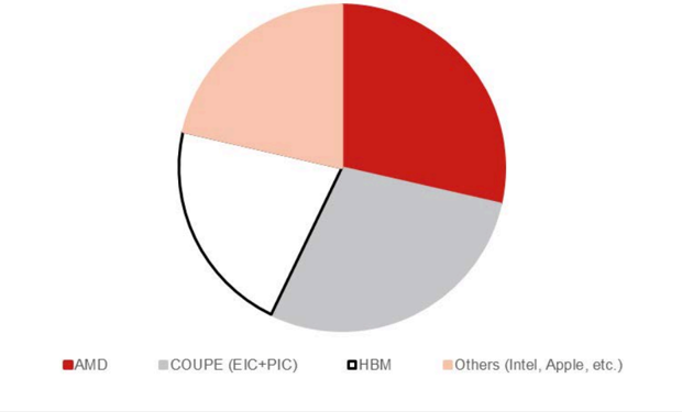
AMD
Source: Nomura estimates
Hybrid bonding potentially requires more sophisticated chip-to-chip/wafer bonders. Although wafer bonding is not a new technology as it has been used for MEMS or CIS (CMOS image sensor) with a 3D stacking structure for years, it would be more complicated if it is used on chiplets, as there could be multiple ICs integrated together (chip-to-chip bonding). The hybrid bonding equipment requires high precision, with placement deviation of less than 0.2um. The more ICs are integrated in the chiplets, the lower the throughput and the greater the difficulty in bonding different ICs.
To reach the high accuracy and density of hybrid bonding, there are very stringent requirements on cleanliness and surface flatness as well. Maintaining cleanliness of chips/wafers is the first requirement. Particles come from many steps such as wafer dicing, grinding, and polishing. Any kind of friction also generates particles, which is an issue, especially because hybrid bonding involves mechanically picking up dies and placing them on top of the other chips. The surface of chips/wafers flatness threshold is generally said to be 0.5nm for the dielectric and 1nm for the copper pads. To achieve the correct dishing profile with a high level of surface smoothness, multiple CMP steps combining low and high Cu removal slurries are required; thus, CMP is becoming a critical process for hybrid bonding.
For SoIC wafer dicing, an issue is the particles that are generated from the process. Blade dicing is generally not used as it is the most dirty: resulting in a lot of particles and a lot of yield loss. Laser dicing is a better solution but it generates laser damage on the edge of SoICs. Plasma dicing is preferred to laser and blade dicing as it is a cleaner process with much less damage to SoICs. However, plasma dicing is the most extreme method and is a similar mechanism to etching away the scribe separating the dies, and the throughput of plasma dicing is much slower than blade and laser dicing particularly when the die size of the chips gets bigger.
Fig. 83: Chip to chip/wafer hybrid bonding
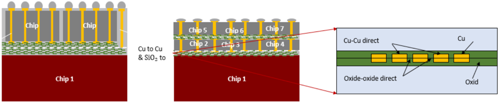
Source: Nomura research
Cu-Cu direct
Oxide-oxide direct
Cu
Oxid
WAFER PREPARATION
Figure
Procedure allemer crumment
Oxide vollratiee
Laser dicing
Plasma dicing
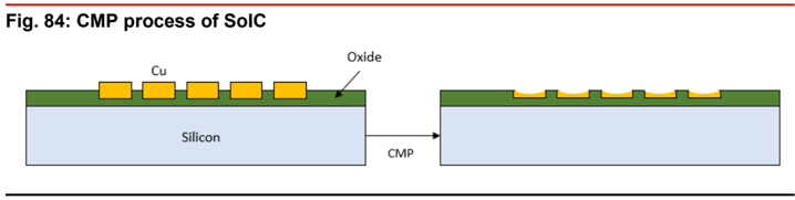
Source: Nomura research
CMP
10 ~ 50 mm/s
Metal
Fig. 85: Comparison of different dicing technologies
Bond Pad wwww
CLEANING
Depend on
PREPARATION
300 mm/s wafer thickness
(Si > 20 um/min)
Higher
| Wafer Chemical | (Chipping or Crack) Mechanical Polishing Wafer | ( Crack or Laser damage) Plasma Wafer Activation | ( Stress free) Repeat |
|---|---|---|---|
| CMP: Ebara Dicing: LAM Research, Disco | Wafercleaning: GPTC Hybrid Bonding: Besi |
Silicon
Source: ITRI, Nomura research
Fig. 86: Process flow and major equipment companies of SoIC
Source: Shraddha Kshirsagar, Nomura research
The die bonder market size of hybrid bonding
According to our calculations, the ASP of the die bonder of hybrid bonding is likely at around USD3m, and we believe Besi is the leader in chip-to-chip/wafer hybrid bonding equipment. The throughput, based on our industry checks, is up to 2000UPH (units per hour). Besi has established a good business relationship with TSMC and Intel and is the clear market leader, in our view. Other players, such as Shibaura (6590 JP, Not rated), are also trying to expand their presence in the hybrid bonding market. Other players worth watching, in our view, are TEL and ASML, which may be able to leverage their solid relationships at the front-end equipment side with TSMC to further explore business
Bond
Chemical
LOW TEMPERATURE BATCH ANNEAL
Interconnect
Server CPU
Server GPU
opportunities in the hybrid bonder market.
TEL
Fig. 87: Hybrid bonder vendors
Numbers of dies in chiplets
The hybrid bonding equipment numbers (units per year)
PC/NB CPU
280
1400
| ASML? 24 | 16 6 16 |
|---|---|
| 82 | 33 174 133 |
| 205 | 83 435 331 |
The market size (USD mn)
Source: Nomura research
Our assumptions on the demand and market size of hybrid bonding equipment are listed in the below table. If chiplets eventually become the standard beyond Moore’s Law, we estimate the market size of hybrid bonding equipment purely would be at minimum of around USD1bn, in addition to the current packaging equipment market of around USD56bn in 2025-26F.
The key variables are:
- Whether only non-mobile CPU (PC/NB/server) will adopt chiplets design, or all mobile CPU will follow eventually? Or only Apple’s CPU will follow? 1.
- What is the actual throughput of hybrid bonding equipment? The throughput may vary along with the complex designs of chiplets. 2.
- How many ICs are in a chiplet? The minimum is two ICs, but this could increase for more complex designs or with a higher integration level. 3.
Fig. 88: Hybrid bonding assumptions
Source: Nomura estimates
HBM4 and beyond
80
Note
It is likely non-mobile CPU and GPU will adopt chiplets design due to larger die size
UPH could be within the range of 800~2000
Two ICs in a chiplets is minimum, it could be higher when the IC is getting more
complicated or with higher integration level
Assuming it is running at 23 hours a day,
25 days a month
Assuming ASP USD2.5mn
FS: 15LM, BS: 4LM
Silicon Carrier
Backside power delivery (BPD) and wafer-towafer technology to drive growth of Semi wafer, wafer bonding, grinding and CMP process
The introduction of backside power delivery
A power delivery network is designed to provide power supply and reference voltage to the active devices on the die most efficiently. Traditionally, it is realized as a network of low-resistive metal wires fabricated through back-end-of-line (BEOL) processing on the frontside of the wafer. The power delivery network shares this space with the signal network, i.e., the interconnects that are designed to transport the signal. Due to the narrower pitches in the signal network, the loss of energy results in a power delivery or IR drop when bringing the power down.
A backside power delivery network is the solution to these issues. The idea is to decouple the power delivery network from the signal network by moving the entire power distribution network to the backside of the silicon wafer, which today serves only as a carrier. From there, it enables direct power delivery to the standard cells through wider, less resistive metal lines, without the electrons needing to travel through the complex BEOL stack. This approach promises to benefit the IR drop, improve the power delivery performance, reduce routing congestion in the BEOL, and when properly designed, allow for further standard cell height scaling.
There are two silicon wafers used in the back-side power delivery process - one is a silicon wafer acting as an interposer (first Semi wafer) in between signal net work, and another acts as the permanent silicon carrier (second Semi wafer) of the device. As such, we expect the usage of silicon wafers to increase along with wafer bonding. On the other hand, the wafer bonding, grinding and thinning process will also increase to form the silicon interposer between the signal and power network (Fig. 89 -90 ).
Fig. 89: Structure of TSMC’s super power rail
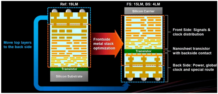
Source: TSMC, Nomura research
STEP 2
Permanent bonding
STEP 3
Backside passivation
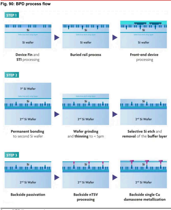
Source: IMEC, Nomura research
The inflection point for BPD should appear in 2027F when TSMC’s starts ramping up A16 capacity
We believe 2027F would be the inflection point for BPD as TSMC’s ramped-up A16 scale drives the dominant share of global BPD capacity and its associated Semi wafer, bonding, thinning, and CMP demand. We expect the majority of the high-performance computing (HPC) chips to adopt BPD technology, while other chips could continue using the normal version node without the BPD function. As a result, for TSMC, we expect its A16 and A12 nodes to be BPD ready, while N2 and A14 nodes are not equipped with the BPD function. By 2030F, global BPD capacity may contribute an additional low-single-digit percentage of total global 12’ semi wafer demand.
150
With BPD
Fig. 91: Key incremental processes required for BPD
Semi wafer
Wafer bonding
Grinding/thinning
0
CMP
Major beneficiaries
Shin-etsu,
SUMCO,
| Siltronic, GWC, | |||
|---|---|---|---|
| wafer 2 back | EVG, TEL, SUSS Microtec, etc. Disco, and | bonding to 2nd Semi New process 2x, additional extrem grind required | |
| 1 back grinding/thinning | grinding/thinning (reduce the thickness of 1st Semi wafer | from 700um to few um only) etc. | potentially Kinik, Ebara, AMAT, |
| 2027F 2028F | 55-70 total 2029F • Other foundries (assuming 30% of the market share) | 20-30% more CMP process per wafer Entegris, Kinik, etc. 2030F | 45-55 total 2026F |
| TSMC backside power delivery capacity (A16, A12) |
Source: Nomura estimates
Fig. 92: BPD capacity of TSMC and other foundries
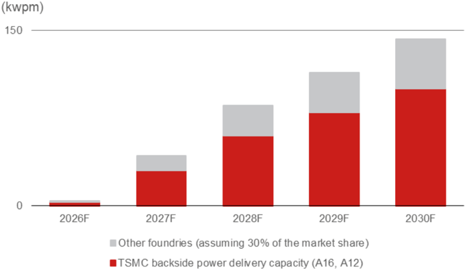
Source: Nomura estimates
Wafer-bonded NAND will also see an inflection point from 2027F driven by NAND makers’ adoption besides YMTC
The wafer-bonded NAND technology was introduced by YMTC for the first time in 2018, YMTC’s wafer-bonded technology is called Xtacking, and can be also called CMOS directly bonded to array (CBA) technology, which makes the CMOS circuit (logic) wafers and memory cells array wafers can be manufactured separately and bonded together. Before the launch of CBA architecture, 3D NAND architectures in the market were divided into traditional side-by-side structure and CnA (CMOS next to Array) architecture.
Since the two types of wafers are manufactured in parallel, there is also the added benefit of shortened production times compared to the conventional method. Performing hightemperature processing solely on the memory cell array wafer makes it possible to achieve the optimal temperature to ensure reliability without having to consider the impact on the CMOS circuit. By separating the wafer manufacturing processes, the performance of the CMOS circuit and the memory cell array can be maximized.
As a result, while YMTC has already adopted CBA technology to produce its 3D NAND since 2018, Kioxia (unlisted) has undertaken some volume production since 2H24 as well. However, we expect Kioxia to further increase its wafer-bonded NAND capacity more meaningfully by the end of 2026F, while Samsung and Hynix will follow by 2027F. We believe it is likely to be positive for the following supply chain sectors:
1 wafer
2 wafers
Multiplier vs. Conventional
2x
The uleamuun opaue arlu
2
1
0
volll waldl uollianlu will ve turo thure
Antoanas.
Faster process time
Memory
Cell Array
- The cleanroom space will increase as more wafer-to-wafer bonding processes are required to produce the same amount of NAND supply. 1. →
- The Semi wafer usage will increase due to the use of additional logic wafers.
- Demand for wafer-to-wafer bonding tool will also increase.
Cu direct bonding
However, the cleanroom space and Semi wafer demand growth would not be 100% but more likely to grow by around 40% more mainly due to the faster front-end process time required to produce each CMOS and memory wafer (Fig. 96 ). By 2030F, global waferbonded NAND capacity may contribute an additional mid-to-high-single-digit percentage of total global 12’ semi wafer demand.
Fig. 93: 3D NAND: CNA vs CBA structure
Source: Kioxia, Nomura research
Fig. 95: YMTC’s Xtacking technology
Source: YMTC, Nomura research
Fig. 96: Wafer-bonded NAND wafer input vs output
The cleanroom space and Semi wafer demand will be 40% more
Source: Nomura estimates
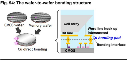
Source: Kioxia, Nomura research
metal VIAs(Vertical Interconnect Accesses)
Cell array
Word line hook up interconnect
Cu bonding pad
Bonding interface
CMOS
Into one wafer
Bit line
LUZO-LIT
90%
80%
70%
60%
50%
40%
30%
20%
10%
0%
module)
SoC for edge Al volung tour deltanu
WoW (WoW hybrid bonding, no interposer
800
W2W Market Share
Alignment Accuracy
Throughput (WPH)
and bump)
70%
700
600
DRAM (LPDDR)
500
SoC for edge Al
400
200
GEMINI FB XT
DRAM (LPDDR)
Fig. 97: Wafer-bonded NAND capacity % Wafer bonded NAND capacity will start to grow more meaningfully from 2026-27F XBS300 W2W 10%
Bandwidth 1024GB/s
100
Bandwidth ~200GB/s
2024F

Source: Nomura estimates
Fig. 99: Major wafer bonding tool suppliers and their specs
Source: Nomura research
DRAM-on-logic wafer-on-wafer (WoW) stacking an emerging trend and could grow meaningfully in 2028F
AI inference is a memory-bound task in the smart-edge domain requiring high memory bandwidth and energy efficiency with the modest compute power in between 45 and100+TOPS. The DRAM-on-logic WoW can achieve 1TB/s bandwidth for throughput higher than 100 TPS (tokens per second). We believe the technology’s strong momentum could start from 2028F, led by AI agents in automotive smart cockpit, premium smartphone/PCs, and robotics.
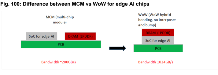
Source: Nomura research
Tools for 10K WSPM
100
80
Fig. 98: Incremental wafer-bonded NAND capacity vs incremental Semi wafer demand vs incremental wafer-to-wafer bonding tool demand
20
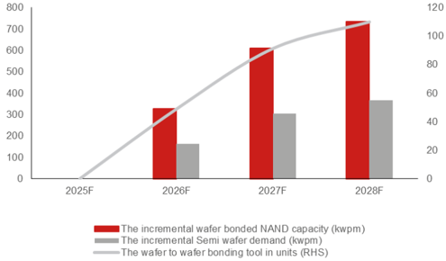
Source: Nomura estimates
Glass core substrate demand could emerge from 2027F at the earliest… but with uncertainty
Glass core substrates and interposers are being pursued intensively by leading device makers, materials suppliers, and equipment vendors for advanced packaging applications. Intel has publicly demonstrated its glass core substrates for next-generation advanced packaging, positioning the work as foundational research for the latter part of this decade rather than imminent high -volume manufacturing, which helps frame expectations for the technology’s maturity today. In parallel, Absolics (unlisted), an affiliate of SKC (unlisted), has secured preliminary US CHIPS Act support to establish a glass -substrate facility in Georgia, signaling real capital formation while still implying multi -year ramps before meaningful production validation. Materials suppliers such as AGC (5201 JP, Neutral), Corning (GLW US, Not rated) and Schott (unlisted) are aligning portfolios and programs around low -coefficient -of -thermal -expansion (CTE) glass and packaging -grade formats, indicating upstream readiness to support trials and early adoption phases.
For AI and high -performance computing (HPC), package footprints, signal counts, and power delivery demands stress organic laminates on warpage, via pitch, and dielectric loss, whereas glass offers the following advantages including:
- Flatness and less warpage 1.
- Better heat dissipation 2.
- Low loss favorable to high -speed signaling 3.
- Large -format integration 4.
The prudent view is that glass interposers and glass core substrates are being actively pursued by credible players, but success remains to be earned in manufacturing and economics.
Through-Glass Vias (TGV): the critical technology of glass core substrate/interposer
Through -Glass Vias (TGV) underpins vertical power and signal paths in glass, typically formed by processes such as laser -assisted drilling and etch, then metallized by full copper fill or sidewall plating with dielectric infill, each bringing distinct stress, planarity, and reliability trade -offs.
High -volume viability depends on repeatable control of via geometry, seed coverage in reentrant sections, void -free metal deposition, chemical -mechanical planarization budgets, and crack suppression during thermal cycling in thin panels, together with high -speed, 100% in -line inspection capable of covering panels that can contain over a million vias to prevent undetected defects from escaping into downstream steps. Hence, it is critical to reach the aspect ratio of over 10:1 level compared with the existing mature technology of 5:1 level, in our view.
Progress has been steady across drilling physics, plating chemistries, and metrology, but we believe the industry is still converging on stable, transferable process windows that remain robust under production variability.
Broadcom’s switch ASIC is likely the pioneer of glass core substrate
We believe Broadcom is likely to be one of the early movers in adopting glass core substrate by 2027F at the earliest, which may be first adopted on its switch ASIC. The main reason why Broadcom is considering the use glass core substrate is mainly to avoid the heat issue which could result in the warpage of substrate. By using the glass core substrate, it can be a good heat spreader with better heat dissipation through copper pillars, in our view.
We expect leading substrate makers such as Unimicron (3037 TT, Buy) to possibly work on glass core substrate development while Broadcom has also invested in a substrate production factory with Toppan (7911 JP, Buy) in Singapore. We are also seeing possible supply chain partners including Schott as a major glass material supplier, with DR Laser (300776 CH, Not rated), Hi-Nano Optoelectronics (unlisted), Spirox (3055 TT, Not rated), and Innostars (7828 TT, Not rated) each cooperating with Ingentec for TGV formation.
material
100%
90%
80%
70%
60%
50%
40%
Schott
30%
AGC
20%
Corning
10%
0%
Etching
AO!
Electroless plating
Sputtering
Electroplating or copper pillar mass
transfer
~USD200
Fig. 101: Process of glass substrate and some supply chain names related to Broadcom
10000
70000
IC
IC
Glass core substrate
PCB
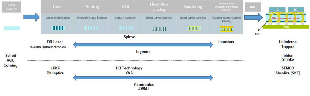
Source: Manz, Nomura research
Uncertainty 1: Cost and technical issues are not fully resolved yet
According to our estimates, currently the TGV process with only a small trial production volume can charge USD400-500 per unit, which means the total ASP of a glass core substrate is likely to be over USD1,500 per unit, which is significantly more expensive than the large-size ABF substrate of around USD200. Thus, we assume that the glass core substrate’s ASP - once it enters mass production - should fall to USD400 at least, otherwise it would not be competitive in terms of cost (Fig. 102 ).
Another issue is the RDL (redistribution layer) dielectric peeling and delamination issue, which is currently the technology bottleneck at the substrate maker side. Once the TGV process is done, the glass core with copper pillars embedded needs to be sent to substrate makers to form the RDL to complete the overall glass core substrate production. However, the CTE (coefficient of thermal) mismatch and surface adhesion challenges in between different materials including glass, ABF and copper are fundamental physics issues, not just engineering refinements. As a result, most of the substrate makers are not aggressively pushing forward the mass production of glass core substrate at this moment (Fig. 103 ).
Fig. 102: Potential BOM cost of glass core substrate vs ABF substrate
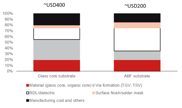
Source: Nomura estimates
ROL
ABF)
Fig. 103: RDL dielectric peeling and delamination issue on glass core substrate
nismatch circuits
Torch
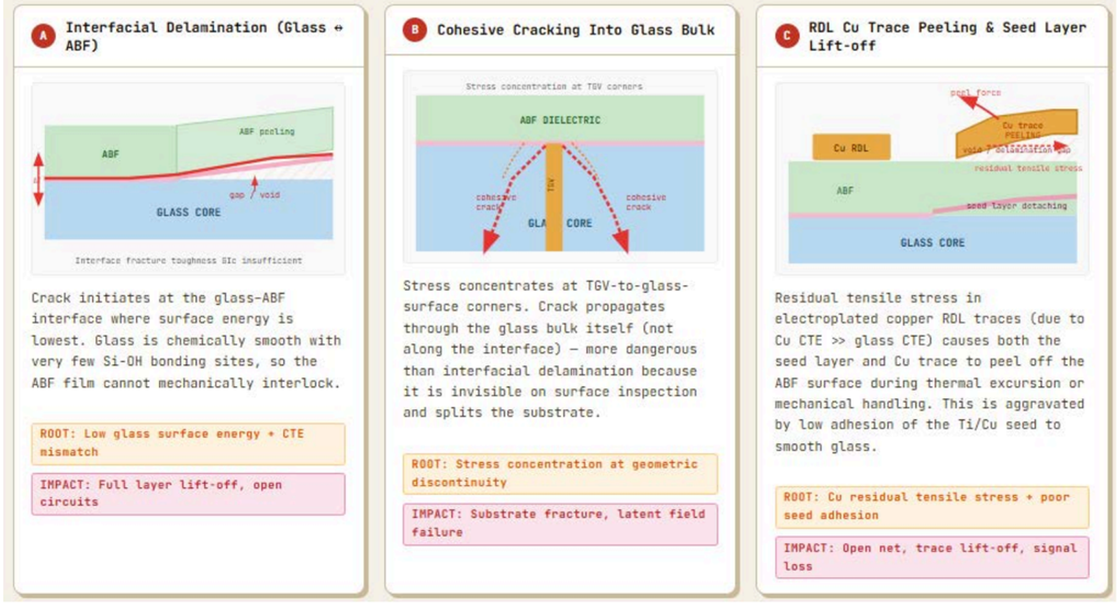
Source: Nomura research
Uncertainty 2: Leading substrate companies are prioritising Intel’s EMIB-T; Broadcom may need to provide more incentives
Intel first introduced its ‘embedded multi-die interconnect bridge (EMIB)’ in 2017 which utilizes silicon bridges buried in the build-up layers of an IC substrate to connect chiplets on top without any interposer (Fig. 104 ). Intel has brought EMIB to several internal products since then (Fig. 105 ), and announced to open its advanced packaging technology portfolio to external customers in 2021, as part of its Intel Foundry/IDM 2.0 strategy. We believe Alchip’s (3661 TT, Buy) AWS Trainium project was the first external customer of Intel Foundry’s EMIB that sought an alternative to TSMC’s CoWoS, aligning with the start of advanced packaging revenue in 2Q24 flagged by Intel’s management.
Although we believe TSMC could aim its 2026F CoWoS supply target towards 2mn wafers a year in response to AI customers’ strong bookings, due to concerns about insufficient capacity support, customers have started evaluating second sources such as OSATs and possibly Intel (Asia Semi & Server anchor report ). Our supply chain feedback suggests Intel’s value propositions against the current constrained supply backdrop could lie in: 1) its 2.5D integration experiences in cost-effective EMIB (despite mostly internal uses) and roadmap to stitch larger, more chiplets; and 2) ‘made in America’ amidst reshoring needs. We have observed that MediaTek’s (2454 TT, Buy) next-generation Google TPU project in 2027F could potentially adopt Intel’s ‘EMIB-T’ package.
Compared with the existing EMIB, the new EMIB-T technology aims to incoporate through-silicon vias (TSVs) within the bridge die to create a vertical power delivery network, thereby shortening the routing distance to imporve power delivery efficiency and performance. According to Intel, EMIB-T targets HBM4/4E and logic chiplet interconnectivity with the lowest possible cost, and the company’s roadmap is to scale to the integration of >8x reticle size total top silicon area on a ~120x120mm substrate by 2026E and >12x reticle size top silicon area on a >120x180mm substrate by 2028E (Fig. 106 ). In addition, the process flow of EMIB-T is not significantly different from conventional EMIB, except that the TSV bridge dies are placed into substrate cavities with solder joint formation.
Cohesive Cracking Into Glass Bulk
RDL Cu Trace Peeling & Seed Layer
Lift-off
Kaby Lake-G
Cross sectional view of EMiB connectivity
Launch time Remarks
Client CPU
Integrates Intel Kaby Lake CPU, AMD Radeon
2017
Fig. 104: An illustration of EMIB
Al accelerator
Al accelerator
Cancelled
2026-27E
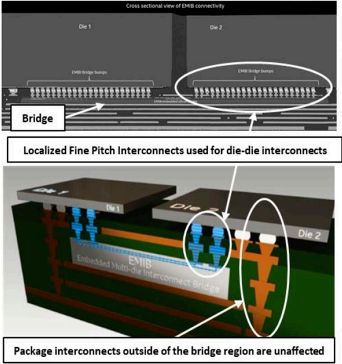
Jaguar Shores
Sapphire Rapids
Emerald Rapids
Granite Rapids
Sierra Forest
Diamond Rapids
Clearwater Forest “Server CPU
Bridge
Coral Rapids
Stratix 10
Agilex
Source: Intel, Nomura research
Fig. 105: Intel’s internal products based on EMIB interconnects
Source: Intel, Nomura research
RX Vega M GPU, and HBM2.
Die 2
Co-EMIB (3.5D); 11 EMIB dies.
vve expell these procurements die mally univell vy cMid-!
-4x
Reticle
1
SizO
2
3
4
5
6
GRAND TOTAL (Apr-May 2026)
2023
2026
Date
Fig. 106: Intel’s EMIB scaling roadmap
size
Future
Purpose
-241x240
Amount
(TWDmn)
38
40 x+
EMIBS
200+
Reticle size
Package size
EMIBS
1,303 Bonder
303 Plant facilities
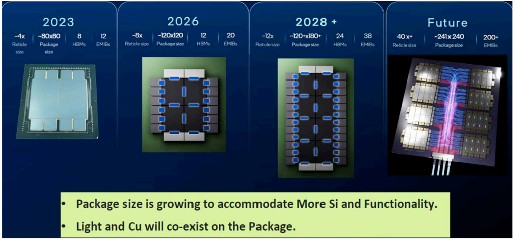
Source:Intel, Nomura research
We believe due to Intel’s strong commitment to leading substrate partners such as Ibiden, Unimicron, and Shinko to bring the EMIB-T technology into mass production, the leading substrate companies are expanding their capacities for Intel aggressively through coinvestment, which could place glass core substrate at a lower priority than EMIB-T. Unimicron has recently announced multiple capex spending on procuring equipment from Toray and ASMPT NEXX, which we believe is mainly for EMIB-T capacity expansion ( Fig. 107 ). As a result, if Broadcom is really committed to bring glass core substrate into mass production, we think it would be better if the company co-invests in capacity with its supply chain partners and provide more incentives; otherwise, the supply chain partners may not be able to ramp up their capacity smoothly considering the lack of resources and funding for glass core substrate production.
Fig. 107: Unimicron’s fixed asset procurement in April-May 2026
We expect these procurements are mainly driven by EMIB-T
Source: MOPS, Nomura research
12
HBMs
20
EMIBS
Counterparty
2028 +
-12x
Reticle size
~120+x180+
24
Package size
HBMs
InP
InP substrate and Photonics SOI wafers are key materials for optical communications
Optical signal
Driven by global AI leaders’ buoyant demand for high-speed optical transceivers, as well as persistent component shortages (i.e., optical chips), we believe the product upcycle will continue into 2027F. Meanwhile, product innovation in the optical transceiver market is accelerating, and future technology trends including silicon photonics (SiPh), LPO/LRO, and NPO/CPO primarily target higher performance, lower energy consumption and costs. We believe 1.6T upgrade and SiPh migration are the key drivers. We think NPO/CPO technologies will continue to improve. If leading CPO solution providers use bundled sales strategies for their CPO switch products, which could accelerate adoption rates in scaleout network in the medium term, while we believe there are more CPO use cases in the scale-up network in the long term.
Other than using silicon-based wafers are used to produce key ICs in optical transceivers, other critical areas where non-siIicon based wafers/materials are used include: 1) InP for EML and CW lasers; 2) Ge (germanium) on silicon for PD and EIC; and 3) photonics SOI wafer for PIC (SiPh); 4) GaAs for driver in EIC; 5) LiNbO 3 for modulator in PIC. Ideally, the fully-integrated PIC necessitates a monolithic III-V compound Semi and silicon platform for efficient light coupling and large dimension III-V compound Semi materials for flexible device/circuit designs. Thus, we believe a monolithic InP/photonics SOI platform for integrated photonics is becoming a better solution. These InP crystals are located right on top of the buried oxide layer and feature an in-plane configuration with the silicon device layer, which results in a unique InP-on-insulator architecture and allows for strong light confinement within the epitaxial InP.
Fig. 108: Structure of an advanced optical transceiver and key materials
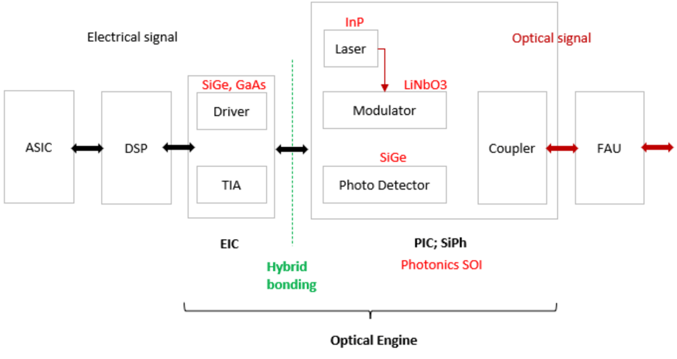
Source: Nomura research
FAU
Fig. 109: SOI-based PIC platform
129tm
SMF2B
Photon
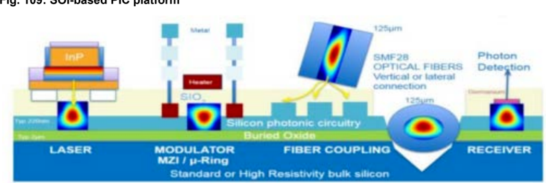
Source: Soitec
Devices)
CPO with
Advanced
Chiplet
(Silicon
Photonic)
CPO with
Holy Grail
Silicon
Photonic
Chiplet
…
Fig. 110: Different formation of CPO
Signal
Fibers
Optical Signal
Fibers
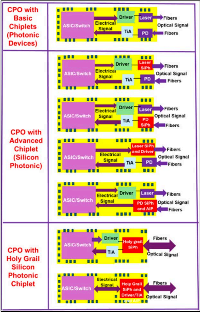
Source: Journal of Microelectronics and Electronic Packaging, Nomura research
InP epi wafer supply and demand outlook - capacity not fully utilized yet, but is tightening
Due to the quickly surging demand from optical transceivers and new CPO switch solutions, we expect upstream material supply shortages to shift from InP epi wafers to InP substrates and then photonics SOI wafers. Below are our InP epi wafer supply/demand assumptions:
- For InP epi wafer capacity expansion, we are assuming the supply will be partially capped by InP substrate supply and the long MOCVD equipment lead time which could be more than one year. 1.
- General speaking, the leading IDMs’, such as Lumentum (LITE US, Not rated) 2.
Driver
TIA
Laser
PD 4
30mm
Die size of SiPh- based PIC
90mm
2,500
2,500
2,000
1,500
2,000
1,000
500
1,500
1,000
0
(3” eq. epi wafers)
2,000
and Coherent (COHR US, Not rated), InP epi wafer utilization rate is running tight, but the merchant players are not yet. Thus, there is still idle capacity in the market. 1,200
- China-based suppliers’ capacity expansion would also have an impact on the supply assumption, as they usually tend to be more aggressive in terms of capacity expansion during the upcycle. 3. 2024 2030
200
- InP epi wafer demand is mainly driven by EML in conventional optical transceiver and CW Laser in SiPh-based optical transceiver. 4.
• Datacom
2026
2027
2028
• Telecom • RF / Defense
- Some demand such as InP PD and InP PIC will be taken by Ge on silicon and photonics SOI wafers. 5.
60%
We believe it is critical to see which merchant InP EPI wafer companies can receive some order outflows from leading IDM companies like Lumentum and Coherent.
Fig. 111: InP epi wafer supply/demand trend
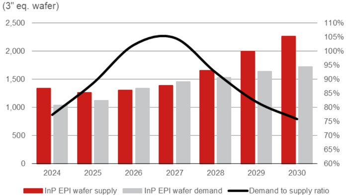
Source: Nomura estimates
Fig. 112: InP EPI wafer capacity by suppliers
Source: Nomura estimates
Fig. 113: InP EPI wafer demand
Source: Nomura estimates
InP substrate supply/demand outlook - the key bottleneck due to low yield rates and Indium export control by China, but may ease in 2028F at the earliest
We expect InP substrate supply would be even tighter than InP epi wafer in 2025-27F considering the 6’ migration with some production yield loss from InP substrate to InP epi wafer. Our other assumptions include:
2029
Other
2030
3,000
4,000
2,500
2,000
3,000
1,500
2,000
1,000
500
1,000
0
0
(3” eq. substrate)
3,500
- For InP substrate, we are assuming the supply will be partially capped by China’s export control on Indium, and also the potentially long equipment move-in lead time. 1.
- The production yield rate of InP laser could be less than 50%. 2.
100%
- China-based suppliers’ will gain more market share in 2028-30F as a key variable to global supply. 3.
- InP substrate demand is mainly driven by EML in conventional optical transceiver and CW Laser in SiPh-based optical transceiver. 4. Freiberger
2026
2027
2028
2029
• ’
AXT / Tongmei
• JX Advanced Metals
• DOWA + WaferTech •
- Some demand such as InP PD and InP PIC will be taken by Ge on silicon and photonics SOI wafers. 5.
We expect the supply shortage will persist in 2025-27F, and gradually ease in 2028F at the earliest.
Source, Nomura estimates
Fig. 115: InP substrate capacity by suppliers - tight supply scenario
Source: Nomura estimates
China Entrants
2030
Fig. 116: InP substrate capacity by suppliers - oversupply scenario
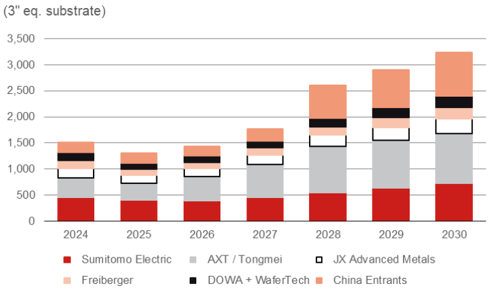
Source: Nomura estimates
(USD)
1500
3,000
2,500
1000
2,000
1,500
500
1,000
500
SOI (12”) pHEMT)
Photonics GaAs (6”
0
Power SOl
USD150
RF, FD, Photonics, imagerSOl depend on specs
USD500
8” ASP USD200~300
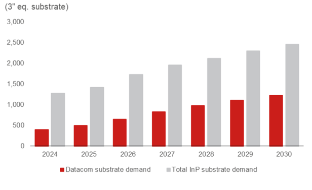
Source: Nomura estimates
Photonics SOI wafer supply/demand outlook - the SiPh PIC would be a new area demand driver; non-photonics SOI wafer market demand is recovering faster than expected
Photonics SOI wafer is becoming an increasing important material to build SiPh-based PIC, due to its scalability in most of the major foundries with lower cost per die. For example, under the same area size, photonics SOI wafer price is only 25% that of InP substrate. Thus, we assume photonics SOI wafer demand will grow along with rising SiPh PIC demand in optical transceivers and CPO modules.
According to our understanding, the PIC die size for a CPO module can reach 50100mm 2 , which may consume more meaningful SOI wafer from 2027F onwards. As a result, we expect that following the InP substrate shortage from 2H25, photonics SOI wafer supply could run tight start from 2027F.
As it is a niche market in terms of the volume shipments, by 2030F, global photonics SOI wafer demand may only contribute a very small portion of total 12’ semi wafer demand. However, the dollar content contribution would be much higher, in our view, since the ASP of photonics SOI wafer is 10x higher than 12’ that for semi wafer.
Other than non-photonics SOI wafer, the rest of RF, FD and Power-SOI have been suffering from weak smartphone and automotive demand for more than one year already. However, we have noticed that recently, customers have been coming back to re-stock those non-photonics SOI wafers due to the concern that AI application will squeeze out the capacity for other applications. As a result, we expect the overall SOI wafer market demand may recover faster than our expectation in our Soitec report ‘The distant leader in photonics SOI’ published in early May.
Fig. 118: Prices of different size and types of substrates
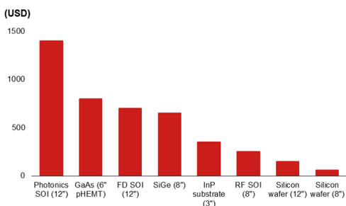
Source: Nomura estimates
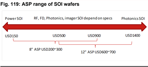
Source: Nomura estimates
USD900
12” ASP USD600~700
Fig. 117: InP substrate demand
USD1400
1,200
1,500
1,000
800
600
1,000
400
200
0
500
0
Fig. 120: Photonics SOI wafer supply/demand trend
2024F|
140.0%
130.0%
(8” eq. k wafers)
1,400
1,200
1,000
800
Source: Nomura estimates
Fig. 121: Photonics SOI wafer capacity by supplier
Source: Nomura estimates
2027F
2028F
2029F
•Pluggable SiPh PIC (70mmz die) = CPO engine PIC (90mmz die)
Others
Fig. 122: Photonics SOI wafer demand breakdown by application
Source: Nomura estimates
12’ semi wafer supply demand could turn more favorable sometime in 2027-28F
We expect there are five major drivers of 12’ semi wafer demand over 2026-30F, including:
- The regular 12’ semi wafer market growing on an average at around 5% per year. ·
- Semi companies’ capacity expansion across leading foundries and memory makers, which could add another 2-3pp growth per year. This incremental growth was seen during the COVID period in 2020-22, when most of the semi companies added capacity to meet rising WFH demand. ·
- Wafer-bonded NAND could add another 1-2pp growth per year, due to additional logic wafer that will be used. ·
- The BPD process and photonics SOI demand could add another 0-1pp growth per year, purely driven by new technology adoption. ·
As a result, it is possible that the 12’ semi wafer demand could grow by around 10% each year from 2026 to 2030F. Assuming most of the leading semi wafer companies reach their capacity limitation by around 2028F, we expect supply-demand could turn more
2030F
30%
14
25%
12
20%
10
8
15%
6
10%
4
5%
2
0
0%
favorable sometime in 2027-28F.
Fig. 123: 12’ semi wafer market growth catalysts
2024
Photonics SOl
100%
95%
90%
Source: Nomura estimates
Fig. 124: 12’ semi wafer supply demand trend
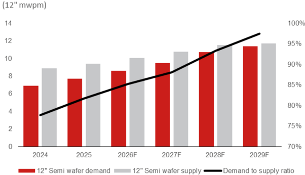
Source: Semi.org, Nomura estimates
Appendix - an introduction to key non-wafer semiconductor materials
Photoresist and photoresist auxiliary
Photoresist introduction
Photoresist is a light-sensitive polymer used for wafer photolithography in IC manufacturing. The photolithography process is the most time-consuming step in the whole IC manufacturing process. During the photolithography process, photoresist will be applied on the wafer surface before the etch process, and it will be dissolved away after it is etched. There are two purpose of the photoresist layers: 1) precise pattern formation, and 2) protection of the substrate from chemical attack during the etch process.
Photoresist is the key material for photolithography, and in manufacturing, the quality has a substantial impact on its performance. Photoresists are usually composed of adhesive agents (~20%), sensitizers (~10%) and solvents (~70%). A good photoresist usually requires high contrast, high resolution and high sensitivity, so that the circuit pattern can be copied precisely to the wafer surface. What’s more, high purity, strong etch resistance, dissolubility, and defined surface tension, density and viscosity are also essential for good photoresist, due to manufacturing engineering standards.
The global photoresist market has long been dominated by companies from Japan such as Tokyo Ohka Kogyo (TOK; 4186 JP, Neutral), and JSR (unlisted).
In terms of different reactions when exposed to UV light, there are two types of semiconductor photoresist: positive photoresist and negative photoresist (Fig. 126 ).
- With positive photoresist, UV light strategically hits the material in the areas that need to be removed. These exposed areas are then washed away by photoresist developer solvent, leaving the underlying material. The areas of the photoresist that aren’t exposed to UV light are left insoluble to the photoresist developer. As a result, there’s an identical copy of the pattern exposed as a mask on the wafer. ·
- Negative photoresist is just the opposite of positive photoresist. The negative photoresist become extremely difficult to dissolve. The UV exposed negative resist will remain on the wafer while the photoresist developer solution works to remove the areas that are unexposed. This leaves a mask that consists of an inverse pattern of the original, which is applied on the wafer. ·
Both positive and negative photoresist are used in the semiconductor manufacturing industry, but more suppliers opt for positive photoresist due to higher-resolution capabilities.
Photoresist auxiliary introduction
- BARC (Bottom Anti-Reflective Coatings; Film) ·
BARC is placed beneath the photoresist layer to prevent light reflection from the substrate. This helps to suppress standing waves caused by interference within the resist layer during exposure, which can lead to variations in sidewall profiles and critical dimensions. As a result, BARC improves the accuracy of lithography.
EBR (Edge Bead Removal) ·
EBR is a process that removes excess photoresist from the edge of a coated substrate, preventing defects that may arise due to non-uniformity. EBR material are the specialized solvent mixtures designed to dissolve and remove excess photoresist.
Developer ·
Developer is a chemical agent used in photolithography to dissolve and remove soluble portions of photoresist, revealing the underlying circuit pattern.
Rinse ·
Rinse material are specialized chemical solutions, often containing surfactants or, in the case of Dry Development Rinse (DDR), functional polymers, used after photoresist development in lithography to prevent pattern collapse.
rg lO
BARC (thinfilm)
photoresist
EBR
• 1. Substrate clean
Photoresist removal ·
- Exposure
Fig. 125: Photoresist and lithography process
Developer
Rinse
Photoresistsolvent
Oxide film
Wafer photoresist is removed to reveal the patterns.
Light source
Photomask
Photoresist removal involves stripping, ashing, or cleaning photoresist polymers after lithography using chemical solvents (Acetone, NMP, DMSO), plasma ashing, or wet cleaning (SPM). UV light
Move Mi
Silicon substrate
Photomask
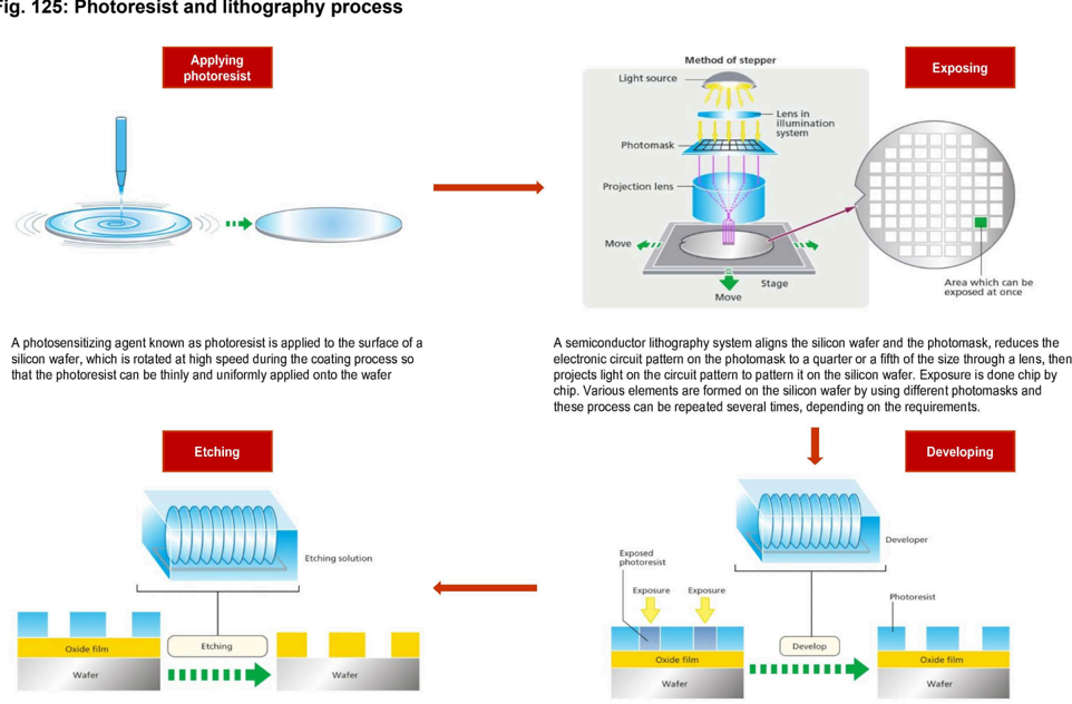
Source: Nikon, Nomura research
Fig. 126: Photoresisting processes
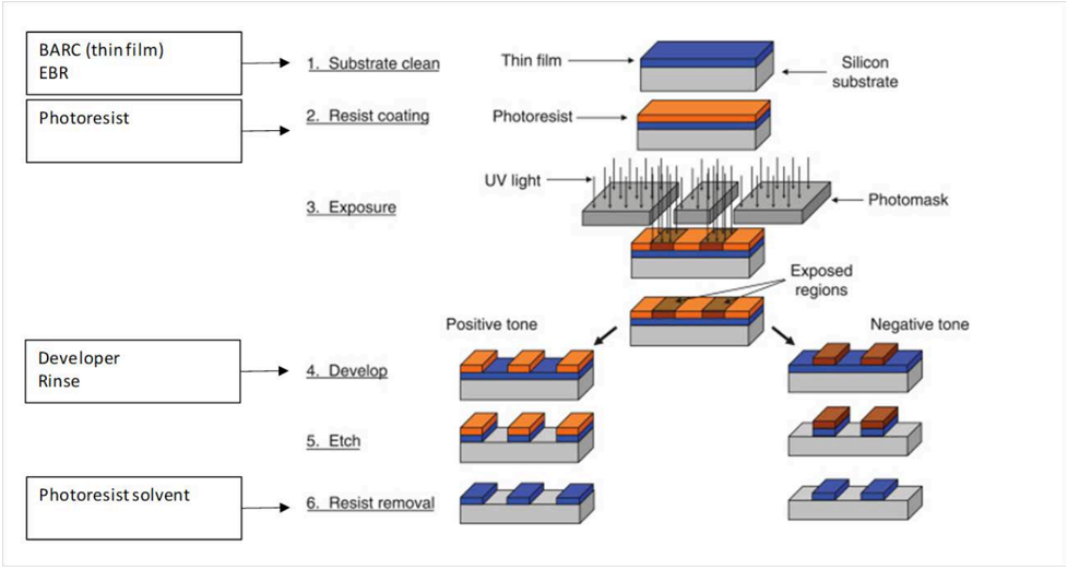
Source: Nomura research
Thin film
Method of stepper
Lens in illumination
system
Exposing
Low
Photoresist
Fig. 127: Technology difficulties of photoresist and auxiliaries
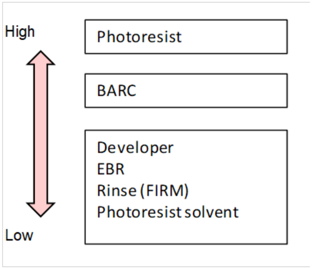
Source: Nomura research
Photomask
A photomask is a quartz or glass substrate coated with an opaque film into which is etched the design of the device being manufactured. In general, photomask has various markets and applications, such as electronic devices, discrete components, light receiving/emitting elements, display devices, MEMS (micro electro mechanical system), and inkjet printers. The manufacturing process normally includes five steps (Fig. 128 ):
- Photomask blanks: an absorber layer with a thickness of tens of nanometers is formed by depositing a substance such as chrome on the quartz substrate. The quartz substrate in this state is called a photomask blank. 1.
- Exposure: Photoresist (photosensitive resin) is uniformly coated over the surface of a photomask blank. Then an LSI circuit pattern is drawn by using an electron beam or a laser beam. 2.
- Development: The portions of resist exposed to the electron beam are removed through the development process (positive tone resist). Depending on the type of resist, there are cases in which non-exposed portions of resist are removed (negative tone resist). 3.
- Etching: The portions from which resist was removed by the development process and the absorber layer is exposed are then etched through a chemical reaction by dry etching. 4.
- Resist removal: A photomask is completed upon removal of the resist and cleaned, and is finally shipped after passing several strict inspection processes. 5.
Photomask Blanks
Fig. 128: Manufacturing process of photomasks
Electron Beam
Development
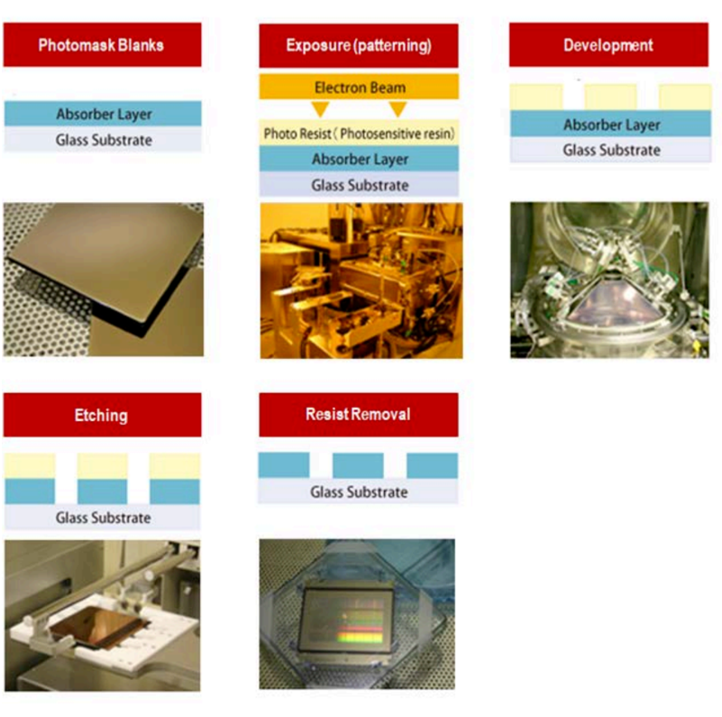
Source: TOPPAN, Nomura research
Photomask technology changes constantly; upstream materials and equipment are dominated by Japan, US, and EU
Photomask technology changes constantly. An independent photomask company needs to understand IC design (fabless) companies’ requirements, as well as gain knowledge on the needs of foundries/IDM’s manufacturing processes. Due to the lack of unified standards in designing processes and different models of equipment from foundries/IDMs, photomasks firms’ competitive advantages lie in R&D and product compatibility with upstream and downstream firms.
- Binary masks (130nm and above): It has a relatively simple structure. It is a photomask blank covered with patterned layer of opaque material. Its transmission characteristics are either transparent or non-transparent. Binary mask is used for building a pattern in which line width is larger than the exposure wavelength. ·
- Phase Shift Mask (PSM) (mature node): PSM has achieved improved wafer printability with higher resolution and increased DOF (Depth of Focus), by controlling the phase shift and the transmission rate. This is a standard technology for lithography, in which line width is smaller than the exposure wavelength. ·
- EUV masks (7nm and below): Unlike conventional DUV, EUV lithography requires reflective optics for wafer exposure systems and for masks, as EUV technology cannot focus light via conventional lens optics (Fig. 129 ). ·
Light Intensity Amplitude
Fig. 129: Photomask classification
EUV light
( 1=13.5nm)
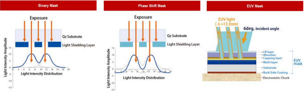
Source: TOPPAN, Nomura research
Photomask equipment suppliers have a higher degree of concentration then those of foundries. The photomask equipment market is mainly dominated by companies from Japan, the US, and Germany (Fig. 130 ). In addition to equipment, photomask raw materials are dominated by companies from Japan and Korea. In order to lower raw materials costs and have better control on product quality and supply chain, leading photomask companies have gradually extended their reach to the upstream raw materials segment (Fig. 131 ).
Fig. 130: Photomask equipment provider
| Category | Process | Major equipment supplier |
|---|---|---|
| Coating | Tokyo Electron (8035 JP), Applied Materials (AMAT US) | |
| Heating | SUSS MicroTec (SMHN DE) | |
| Etching | Applied Materials (AMAT US) | |
| Front-End | Writing | Laser direct writing: Applied Materials (AMAT US), Mycronic (MYCR ST) Electron beam direct writing: Nuflare (Unlisted), IMS (Unlisted), JEOL (6951 JP) |
| Critical Dimension (CD) measurement | Holon (Unlisted), Advantest (6857 JP) | |
| Overlay (OVL) measurement | KLA (KLAC US), Zeiss (Unlisted) | |
| Cleaning | SUSS MicroTec (SMHN DE) | |
| Defect detection | KLA (KLAC US), Nuflare (Unlisted), Lasertec (6920 JP) | |
| Back-End | Defect repair | Hitachi (6501 JP), V Technology (7717 JP), High-end electron beam repair is dominated by Zeiss (Unlisted) |
| Verification | Zeiss (Unlisted) |
Source: Company data, Nomura research
Fig. 131: Photomask raw materials
| Raw materials/Companies | HOYA | LG-IT | DNP | PKL | TOPPAN | SKE | Qingyi | Newway |
|---|---|---|---|---|---|---|---|---|
| Substrate | ✓ | ✓ | x | x | x | x | x | x |
| Chrome | ✓ | ✓ | x | x | x | x | x | x |
| Photoresist coating | ✓ | ✓ | ✓ | ✓ | ✓ | ✓ | ✓ | ✓ |
Source: Company data, Nomura research
Phase Shift Mask
Exposure
EUV Mask
6deg. Incident angle
Electric gas
The process of manufacturing semiconductors requires using different gases at different phases. While common gases such as nitrogen, hydrogen, argon, and helium can be used in their pure form, some processes may require a specialized mixture. Below we list the primary processes of semiconductor manufacturing, and the principal gases used:
- Deposition: is the process that creates the materials found inside electronic devices: the conductors, semiconductors, and insulators. Typically, substrate is heated to an elevated temperature favorable to the desired reaction in a two gas-phase chamber, which results in a thin-film product produced directly on top of the preceding layer. The reaction can be further activated by using an argon or helium plasma. Various different gases are used in deposition steps, and these are chosen as the precursors to the desired thin-film product. Some gases such as ammonia and silane have been used since the beginning of semiconductor fabrication. Others have come into use later, and some have been developed specifically for use in electronics. ·
- Photolithography: is the process that forms the shapes of the devices and is key to the miniaturization of microchips. The lithography tool - called a scanner - acts like a slide projector: it takes the light from a source to transfer an image from a master pattern, etched in a piece of glass, onto the substrate that is covered with lightsensitive chemical films. This image is the pattern that will form the minute circuitry of the microchip. Subsequent wet chemical steps are used to develop the pattern and remove either the exposed or non-exposed portion of the chemical film. ·
- Etching: is the process used to selectively remove materials and usually follows photolithography as a way to permanently realize the pattern and shape made in the lithographic process. Etchant gases are activated in argon plasmas above the substrate and then react with one material at the surface preferentially to another. The reaction products are also gases and are removed through a vacuum system. ·
- Doping: is the process that helps to modify the conductivity of semiconducting materials. By adding atoms of these materials into a previously deposited semiconductor material, the circuit engineer can determine the exact conditions at which the semiconductor layer will conduct electrons. The doping atoms can be added either by allowing gases to react on the surface and diffuse into a heated substrate, or by plasma activation, in which an electric field is used to accelerate them into the substrate. ·
- Annealing: is another process used to modify the composition of an existing thin film. Most often conducted at elevated pressure and temperature, oxygen or hydrogen is reacted with the existing layer to create a new oxide or hydride layer on the surface. In other applications, the substrate with added thin film layers is heated and cooled so that the top-most thin film can form a crystaline phase. ·
- Chamber cleaning: is an important process to keep chambers in working conditions. Excess chemical reactants and products deposit not only on the substrate, but also on the chamber walls and other equipment inside the process chamber. Because of the sensitive dimensions of electronic devices, even small particles produced from these excess materials can ruin devices under fabrication. In between process steps, halide gases are plasma are activated to react with and remove the excess materials, like an etching step for the entire inside of the process chamber. ·
Lithography
Fig. 132: Semiconductor manufacturing processes and gases used
Nitrogen gases: NH3, N20
Oxygen: 02
Tungsten hexafluoride: WF6
Germane: GeH4
By diffusion
(neutral particles)
Hydrides: AsH3, BF3, B2H6, PH3, GeH4, Ge2H6
Etching
Source: Linde, Nomura research
Fig. 133: Processes and gases used
| Processes | Deposition | Lithography | Etching | Doping | Annealing | Chamber cleaning |
|---|---|---|---|---|---|---|
| Gases used | Nitrogen gases Silicon gases Oxygen Tungsten hexafluoride Germane | Laser gases Carbon dioxide Hydrogen | Fluorocarbons Sulfur hexafluoride Halides Oxygen | Hydrides | Oxygen Hydrogen Argon | Nitrogen trifluoride Other fluoride gases Chloride gases Fluorine |
Source: Linde, Nomura research
By category, gases in electronics manufacturing can also be divided into two groups for the purpose of supply:
- Bulk gases - nitrogen, oxygen, argon, helium, hydrogen, and carbon dioxide - are six gases that are both used in large amounts and commonly sourced from industrial supply chains. These are normally stored in tanks or containers to ensure adequate supply. ·
- Electronic special gases are all other gases and number over a hundred in pure and specialty mixtures. These can be supplied in sizes from small lecture bottles to containers, depending upon process demand. All of these require additional levels of purification and quality control well beyond that of other industrial processes. ·
Fig. 134: Gases in various technology sectors
| Sector | Materials |
|---|---|
| Semiconductor | Bulk gases: argon, carbon dioxide, helium, hydrogen, nitrogen, oxygen Most common specialty gases: nitrogen trifluoride, tungsten hexafluoride, hydrogen chloride, ammonia, disilane, germane, high purity carbon dioxide, nitrous oxide |
| Display | Bulk gases: argon, carbon dioxide, helium, hydrogen, nitrogen, oxygen Electronic special gases: cleaning (fluorine and nitrogen trifluoride), deposition (ammonia, nitrous oxide, and silane), doping (diborane and phosphine), etching (boron trichloride, chlorine, octafluorocylobutane, pentafluoroethane, sulfur hexafluoride, and tetrafluoromethane), laser (fluorine/hydrogen, hydrogen chloride/hydrogen/neon, krypton, neon, and xenon) |
| Solar | Bulk gases: argon, helium, hydrogen, nitrogen, oxygen Electronic special gases: silane, ammonia, fluorine (on-site generation), sulphur hexafluoride, chlorine, carbon tetrafluoride, arsine and phosphine mixtures |
Source: Nomura research
Chemical Mechanical Planarization (CMP) slurry, pad and conditioner
CMP slurry introduction
Chemical Mechanical Planarization, or CMP, is a polishing process that utilizes a chemical slurry formulation and mechanical polishing process to remove unwanted conductive or dielectric materials on the silicon wafer, achieving a near-perfect flat and smooth surface upon which layers of integrated circuitry are built (Fig. 135 ). CMP slurry consists of abrasive particles and chemical components such as pH adjuster, dispersant, polymeric additives, oxidizer, and a passivation agent, depending on polishing purpose, to provide proper surface modification of material. According to different manufacturing and technology requirements, each wafer will go through multiple or dozens of CMP processes. The global CMP industry has long been dominated by companies from the US and Japan.
Abrasive particles in the polishing slurry are essential for polishing, and the size of the particles used in polishing has been shown to have an effect on the rate at which material is removed from the surface. Common materials of abrasive particles in CMP slurries are silicon dioxide, tungsten, and copper. Tungsten CMP is generally used for the memory IC process, while copper CMP is mostly applied in the 130nm and more advanced nodes of logic IC. In addition, as IC manufacturing processes evolve and become more complicated, we expect demand for CMP materials will accelerate. For instance, 65nm node technology needs 15 CMP processes, while 14nm requires 28 CMP processes. The 1.6nm IC manufacturing technology needs 70 CMP processes (Fig. 138 ).
The basis chemical compositions of CMP slurry are (Fig. 136 ):
- Abrasive particle: polishes the surface of a wafer and removes unwanted substances and metals. ·
- Oxidizer: a chemical substance that removes an electron from a metal surface. ·
- Chelating agent: forms complexes with metal ions. ·
- Corrosion inhibitor: provides metal corrosion protection. ·
- Surfactant: changes the properties of the water surface. ·
- pH adjustor: controls the pH of the slurry. ·
Head pressure
Wafer
(Upside down)
Rotating head
Source: Fujifilm, IntechOpen, Nomura research
Fig. 136: Composition of CMP slurry
| Composition | Description |
|---|---|
| Abrasive particles | Abrasive particles are essential for polishing the metal surface. For polishing silicon and silicon-based materials, colloidal silica (silica gel) or other metal oxides such as ceria are typically used. Abrasive particles’ size, concentration, and interaction with other chemical materials all influence the polishing performance. |
| Oxidizer | The oxidizer is a substance that has the ability to oxidize other substances, facilitating mechanical polishing on the wafer. |
| Chelating agent | The chelating agent forms complexes with metal ions. A combination of the oxidizer and chelating agent would help to obtain a better passivation layer and high dissolution rate of the metal. |
| Corrosion inhibitor | The corrosion inhibitor is a chemical compound that decreases the corrosion rate of a material which comes into contact with the fluid. The CMP process can obtain perfect surface planarity, only if the concave surface of the wafer is properly protected from corrosion by the corrosion inhibitor. |
| Surfactant | Surfactants are compounds that lower the surface tension, or interfacial tension, between two liquids. In the CMP process, surfactants can enhance the cleaning process. |
| pH adjustor | The pH adjustor is to adjust the pH of CMP slurry so as to improve the removal rate of the CMP slurry. |
Source: Nomura research
CMP pad introduction
CMP pad is an innovative pad used in the Chemical Mechanical Polishing (CMP) process for advanced node semiconductor manufacturing, especially after the PVD (physical vapor deposition) process. A CMP pad is made of a loose and porous structure that comprises a matrix consisting of fibers. The polishing pad surface has voids in which polishing slurry flows during chemical mechanical polishing of substrates, and in which debris formed during the chemical-mechanical polishing of substrates is temporarily stored for subsequent rinsing away. CMP pads help in the application of CMP slurries evenly on wafers and improve the stability and efficiency of planarization. CMP pads are consumable materials, with normal usage life of 45-75 hours. Memory chips are the largest downstream applications of CMP pads.
CMP conditioner (diamond disk) introduction
During the CMP process, the pad surface becomes smooth and glazed due to mechanical compression from wafer contact and the particle and chemical buildup from slurry residues, reducing pad roughness and slurry flow, leading to lower removal rates and the risk of non-uniform polishing. Therefore, CMP pads need to be reconditioned continuously to extend their useful life. The pad conditioner (or diamond disk) would mechanically scrape the pad surface to reopen pores for slurry distribution, regenerate micro-asperities to restore surface texture, and remove glazed material.
We estimate the semiconductor CMP pad conditioner market size was ~USD400mn in 2025 at moderate supplier concentration with 4-6 significant players controlling a combined 70-80% market share, including Asahi Diamond (6140 JP, Not rated) supplying Japan domestic customers, TSMC, 3M (MMM US, Not rated) across major foundries and memory makers, and SAESOL Diamond (unlisted) for Samsung and Hynix.
(Il)
80
70
60
50
40
30
20
10
0
Polishing slurry
Polishing pad
ANODE O
Fig. 137: CMP pad and conditioner in CMP process
Head
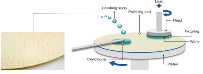
Source: Sensofar Metrology, Nomura research
•CMP steps
Fig. 138: CMP processes vs IC technology nodes
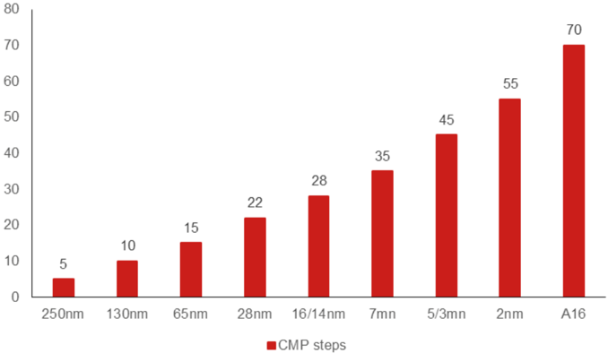
Source: SEMI, Nomura research
Target
Sputtering is a technology used to form a thin film on a silicon wafer, glass, or other substrate. Within a vacuum state maintained in a sputtering machine, a sputtering target is bombarded with argon ions. This causes atoms or molecules to be emitted from the sputtering target. The atoms or molecules are deposited and form a thin film on the substrate. Sputtering targets are materials from which thin films are grown by the sputtering method, and the targets are fabricated by processing metals or ceramics (Fig. 139 ).
Fig. 139: Sputtering process
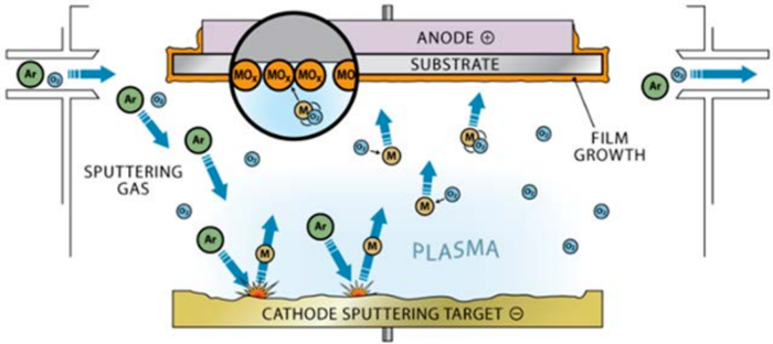
Source: INF Wiki, Nomura research
7mn
5/3mn
2nm
A16
Load
70
In terms of process, the sputtering target is used for the fabrication of the barrier layer and the packaging metal wiring layer.
- In the wafer manufacturing process, the target material is mainly used to make the wafer conductive layer, barrier layer, and metal grid. ·
- In the chip packaging process, the sputtering target material is used to generate the metal layer under the bump, wiring layer, and other metal materials. ·
The amount of target materials used in wafer manufacturing and chip packaging is small; according to SEMI statistics, the cost of target materials in wafer manufacturing and packaging process accounts for about 3% of Semi material market. However, the quality of sputtering target materials directly affects the uniformity and performance of the conductive and barrier layers, and further affects chip transmission speed and stability, so sputtering target materials are considered by many to be the core raw materials for semiconductor production.
Sputtering target in semiconductor: increasing demand for aluminum, titanium, tantalum, and cooper
By chemical composition, sputtering target materials can be divided into metal target materials (pure metal aluminum, titanium, copper, and tantalum), alloy target materials (nickel-chrome alloy and nickel-cobalt alloy) and ceramic compound target materials (oxides, silicides, carbides and sulfide). By application, they can be divided into semiconductor chip target materials, planar display target materials, solar cell target materials, information storage target materials, tool modified target materials, electronic device target materials, and other target materials.
In semiconductor wafer manufacturing, the manufacturing process of 200mm (8-inch) and below wafers is usually mainly made of aluminum, and the target materials used are mainly made of aluminum and titanium. However, the manufacture of 300mm (12-inch) wafer mostly uses advanced copper interconnection technology and mainly uses copper and tantalum target materials. Overall, as the use of chips becomes more and more extensive and chip demand increases, we expect demand for aluminum, titanium, tantalum and copper, the four mainstream thin-film metals in the industry, to also increase. There is currently no alternative to these four thin-film materials, either technically or economically, so we do not believe they are at risk of being replaced. Fig. 140 shows the main types, uses, and performance requirements for sputtering targets in the electronics field.
Fig. 140: Types and applications of sputtering targets in the electronic industry
| Type | Application | Main variety | Performance requirements |
|---|---|---|---|
| Semiconductor | Used to prepare integrated circuit core materials | W, WTi, Ti, Ta, Al alloy with purity 4N or 5N | Highest technical requirements; ultra- high purity metal; high precision size; high integration |
| Flat display | Sputtering technology guarantees uniformity of film produced, increases productivity and reduces costs | Nb, Si, Cr, Mo, MoNb, Al alloy , Cu and Cu alloy target | High technical requirements; high purity materials; large material area; high uniformity |
| Decoration | Used for coating the surface of the product for beautification, wear resistance and corrosion resistance | Cr, Ti, Zr, Ni, W, TiAl, CrSi, CrTi, CrAlZr target | General technical requirements; mainly used for decoration, energy-saving, etc |
| Tool | Enhance the surface of tools and molds, improve the life and the quality of the parts manufactured | TiAl, CrAl, Cr, Ti, TiC, Al2O3 target | High-performance requirements; extended service life |
| Solar | Sputter coating technology for the production of fourth-generation thin-film solar cells | ZnOAl, ZnO, ZnAl, Mo, CdS, CIGS target | High technical requirements; large application range |
| Electron device | Thin-film resistors, film capacitors | NiCr, NiCrSi, CrSi, Ta, NiCrAl target | Requires small size, good stability, and low-temperature coefficient of resistance |
| Information storage | Used to make storage | Cr alloy, Co alloy, CoFe alloy, Ni alloy | High storage density; high transmission speed |
Source: Stanford Advanced Materials, Nomura research
High entry barriers: dominated by Japan and US firms
Sputtering coating technology originated from the US and Japan, and the required sputtering target products have high-performance requirements, so research and production have mainly been concentrated in a few companies in those countries. The
application fields of sputtering target mainly focus on the semiconductor, flat-panel display (including touch screens) and solar cell industries.
Target manufacturing has high entry barriers, which are mainly reflected in technology, clients verification, and raw materials supply.
- Manufacturing: target manufacturing has high requirements in terms of companies’ R&D and manufacturing processes. ·
- Verification cycles: clients normally have long verification cycles and various verification requirements. In general, it takes 2-3 years for targets to reach mass shipment. Moreover, newcomers need to continuously improve their product quality and manufacturing capabilities to win bidding or increase their supply share. ·
- Raw materials: along the supply chain, raw materials providers normally have strong bargaining positions. For a long time, Chinese target manufacturers have mainly obtained high-purity metals by importing them from overseas. ·
Due to high entry barriers and large capex requirements, there are limited players in the high-purity sputtering target industry, which is mainly dominated by Japan and US firms.
Relative performance chart
EQUITY: TECHNOLOGY
Price
(TWD)
500-
400-
3001
200-
100
- 300
-250
-
200
-
150
Ingentec Corporation 4768.TWO 4768 TT
EQUITY: TECHNOLOGY
Churra. I CEC Namura
Glass core substrate potential yet to be fully unlocked
Take-off of glass core substrate business could be seen on top of improving specialty gas business
Action: Initiate coverage at Buy with TP of TWD960
We initiate coverage of Ingentec, a Taiwanese specialty gas supplier and emerging TGV (ThroughGlass Via) glass core substrate manufacturer, with a Buy rating. In our view, Ingentec is positioned at the intersection of two powerful secular trends: 1) the accelerating demand for etch gases driven by memory capacity expansion, particularly 3D NAND; and 2) emerging glass core substrate demand driven by Broadcom from 2027F. We estimate 2026F will be a year of recovery for its core specialty gas business, and glass core substrate business could emerge from 2027F onwards. Thus, we assume there could be more meaningful sales and earnings growth in late 2027F. Our target price of TWD960 is based on 60x 2028F EPS TWD16, in the mid-range of the company’s 45-75x P/E over 2021-23, when Ingentec’s specialty gas business was strong, driven by tight supply due to the Ukraine-Russia war. We expect Ingentec’s sales to see a 129% CAGR in 2026-28F. The stock is trading at 31.7x 2028F PE. Downside risks include: 1) a weakening Semi CAPEX cycle; 2) losing market share to competitors; 3) commercialization delay in next-generation products; and 4) the adoption of glass core substrate is slower than expected.
Specialty gas business: likely driven by memory capacity and the leading foundry’s capacity expansion
Ingentec’s core business is specialty gas such as C 4 F 6 and C 4 F 8 mainly used in Semi etching process. Although Ingentec’s largest customer is a leading foundry in Taiwan, the more specialty gas usage will be mainly driven by memory customers in Japan and Korea. 3D NAND is particularly the important driver because it has more etching processes over DRAM and advanced logic chips. As a result, if memory companies start to expand capacity in the coming quarters, Ingentec’s specialty gas business should see a profound recovery from current levels, as memory companies are mostly not expanding capacity until later-2026F.
Glass core substrate business: the expert of TGV technology
Ingentec has been developing substrate-related materials and processes for microLED since 2017, and has leveraged related studies and patents onto glass core substrate. Ingentec’s patented TGV technology, LADY (Laser Arrow Decomposition Yield), applies a fine chemical distillation technology to produce ultra- high purity specialty gases, which are introduced into advanced processes such as dry etching, film removal, and precision glass drilling. Whether Broadcom adopts glass core substrate o not in 2027-29F is worth monitoring, in our view.
| Year-end 31 Dec Currency (TWD) | FY25 Actual | Old | FY26F New | Old | FY27F New | Old | FY28F New |
|---|---|---|---|---|---|---|---|
| Revenue (mn) | 1,229 | 0 | 1,788 | 0 | 2,531 | 0 | 9,337 |
| Reported net profit (mn) | 19 | 0 | -24 | 0 | 246 | 0 | 1,174 |
| Normalised net profit (mn) | 19 | 0 | -24 | 0 | 246 | 0 | 1,174 |
| FD normalised EPS | 39.34c | -51.44c | 4.09 | 16.20 | |||
| FD norm. EPS growth (%) | -86.4 | -230.8 | - | 296.4 | |||
| FD normalised P/E (x) | 1,094.4 | - | - | - | 105.3 | - | 26.6 |
| EV/EBITDA (x) | 143.5 | - | 230.1 | - | 27.4 | - | 13.2 |
| Price/book (x) | 11.9 | - | 13.6 | - | 2.2 | - | 2.1 |
| Dividend yield (%) | 0.9 | - | 0.9 | - | 0.7 | - | 0.9 |
| ROE (%) | 1.0 | -1.5 | 3.2 | 8.1 | |||
| Net debt/equity (%) | 56.4 | 105.8 | net cash | 12.6 |
Source: Company data, Nomura estimates
Global Markets Research 21 May 2026
| Rating Starts at | Buy |
|---|---|
| Target price Starts at | TWD 960.00 |
| Closing price 15 May 2026 | TWD 430.50 |
| Implied upside | +123.0% |
| Market Cap (USD mn) | 648.0 |
| ADT (USD mn) | 25.5 |
Relative performance chart
Source: LSEG, Nomura
Research Analysts
Semiconductor
Donnie Teng - NIHK donnie.teng@nomura.com +852 2252 1439
Aaron Jeng, CFA - NITB
aaron.jeng@nomura.com +886(2) 21769962
Eric Chen, CFA - NITB
eric.chen@nomura.com +886(2) 21769965
Vivian Yang - NITB
vivian.yang@nomura.com +886(2) 21769970
Key data on Ingentec Corporation
Performance
| (%) | 1M | 3M | 12M | ||
|---|---|---|---|---|---|
| Absolute (TWD) | -11.1 | 11 | 305.4 | M cap (USDmn) | 648 |
| Absolute (USD) | -10.8 | 10.5 | 287.3 | Free float (%) | 68.9 |
| Rel to Taiwan TAIEX Index | -23.2 | -11.6 | 215.9 | 3-mth ADT (USDmn) | 25.5 |
Income statement (TWDmn)
| Year-end 31 Dec | FY24 | FY25 | FY26F | FY27F | FY28F |
|---|---|---|---|---|---|
| Revenue | 1,017 | 1,229 | 1,788 | 2,531 | 9,337 |
| Cost of goods sold | -604 | -927 | -1,473 | -1,752 | -6,360 |
| Gross profit | 413 | 303 | 315 | 779 | 2,977 |
| SG&A | -230 | -264 | -336 | -460 | -1,420 |
| Employee share expense | |||||
| Operating profit | 182 | 39 | -20 | 320 | 1,558 |
| EBITDA | 267 | 149 | 96 | 441 | 1,685 |
| Depreciation | -83 | -109 | -114 | -120 | -126 |
| Amortisation | -1 | -2 | -2 | -2 | -2 |
| EBIT | 182 | 39 | -20 | 320 | 1,558 |
| Net interest expense | -4 | -20 | -29 | -29 | -29 |
| Associates & JCEs | |||||
| Other income | 13 | 1 | 12 | 12 | 12 |
| Earnings before tax | 191 | 20 | -37 | 303 | 1,541 |
| Income tax | -37 | -6 | -6 | -76 | -385 |
| Net profit after tax | 155 | 13 | -43 | 227 | 1,156 |
| Minority interests | -23 | 5 | 19 | 19 | 19 |
| Other items | |||||
| Preferred dividends | |||||
| Normalised NPAT | 131 | 19 | -24 | 246 | 1,174 |
| Extraordinary items | |||||
| Reported NPAT | 131 | 19 | -24 | 246 | 1,174 |
| Dividends | -151 | -181 | -181 | -229 | -276 |
| Transfer to reserves | -20 | -162 | -205 | 17 | 898 |
| Valuations and ratios | |||||
| Reported P/E (x) | 148.4 | 1,094.4 | - | 105.3 | 26.6 |
| Normalised P/E (x) | 148.4 | 1,094.4 | -836.9 | 105.3 | 26.6 |
| FD normalised P/E (x) | 148.4 | 1,094.4 | - | 105.3 | 26.6 |
| Dividend yield (%) | 0.8 | 0.9 | 0.9 | 0.7 | 0.9 |
| Price/cashflow (x) | 78.1 | 83.8 | 258.9 | 99.7 | 49.0 |
| Price/book (x) | 10.4 | 11.9 | 13.6 | 2.2 | 2.1 |
| EV/EBITDA (x) | 78.5 | 143.5 | 230.1 | 27.4 | 13.2 |
| EV/EBIT (x) | 114.9 | 552.6 | - | 37.8 | 14.3 |
| Gross margin (%) | 40.6 | 24.6 | 17.6 | 30.8 | 31.9 |
| EBITDA margin (%) | 26.2 | 12.1 | 5.4 | 17.4 | 18.1 |
| EBIT margin (%) | 17.9 | 3.2 | -1.1 | 12.6 | 16.7 |
| Net margin (%) | 12.9 | 1.5 | -1.4 | 9.7 | 12.6 |
| Effective tax rate (%) | 19.2 | 32.6 | - | 25.0 | 25.0 |
| Dividend payout (%) | 114.9 | 968.5 | - | 93.1 | 23.5 |
| ROE (%) | 7.9 | 1.0 | -1.5 | 3.2 | 8.1 |
| ROA (pretax %) | 7.9 | 1.3 | -0.6 | 6.2 | 11.9 |
| Growth (%) | |||||
| Revenue | 24.7 | 20.9 | 45.5 | 41.6 | 268.9 |
| EBITDA | 22.8 | -44.1 | -35.8 | 360.7 | 282.0 |
| Normalised EPS | 15.4 | -86.4 | -230.8 | - | 296.4 |
| Normalised FDEPS | 15.4 | -86.4 | -230.8 | - | 296.4 |
Source: Company data, Nomura estimates
Cashflow statement (TWDmn)
| Year-end 31 Dec | FY24 | FY25 | FY26F | FY27F | FY28F |
|---|---|---|---|---|---|
| EBITDA | 267 | 149 | 96 | 441 | 1,685 |
| Change in working capital | 10 | 162 | 6 | -89 | -647 |
| Other operating cashflow | -28 | -67 | -23 | -93 | -402 |
| Cashflow from operations | 249 | 244 | 79 | 260 | 636 |
| Capital expenditure | -580 | -563 | -536 | -2,579 | -10,621 |
| Free cashflow | -331 | -319 | -458 | -2,320 | -9,985 |
| Reduction in investments | 49 | 16 | 19 | 19 | 19 |
| Net acquisitions | |||||
| Dec in other LT assets | 103 | -7 | -7 | -7 | |
| Inc in other LT liabilities | -3 | 0 | 0 | 0 | |
| Adjustments | -6 | -106 | 7 | 7 | 7 |
| CF after investing acts | -288 | -309 | -438 | -2,301 | -9,966 |
| Cash dividends | -151 | -181 | -181 | -229 | -276 |
| Equity issue | 11 | 1 | 0 | 12,500 | 0 |
| Debt issue | 394 | 762 | 300 | 300 | 0 |
| Convertible debt issue | |||||
| Others | -4 | -7 | -9 | -9 | -9 |
| CF from financial acts | 250 | 575 | 110 | 12,563 | -285 |
| Net cashflow | -38 | 266 | -328 | 10,262 | -10,251 |
| cash | 321 | 10,482 | |||
| Beginning | 283 | 549 | 221 | ||
| Ending cash | 283 | 549 | 221 | 10,482 | 231 |
| Ending net debt | 501 | 965 | 1,593 | -8,368 | 1,883 |
| Balance sheet (TWDmn) | |||||
| As at 31 Dec | FY24 | FY25 | FY26F | FY27F | FY28F |
| Cash & equivalents | 283 | 549 | 221 | 10,482 | 231 |
| Marketable securities | 15 | 1 | 1 | 1 | 1 |
| Accounts receivable | 159 | 241 | 269 | 381 | 1,407 |
| Inventories | 195 | 351 | 484 | 576 | 2,091 |
| Other current assets | 58 | 76 | 76 | 76 | 76 |
| Total current assets | |||||
| LT investments | 710 11 | 1,218 | 1,051 6 | 11,516 6 | 3,806 6 |
| Fixed assets | 1,807 | 6 2,392 | 2,815 | 5,274 | 15,770 |
| Goodwill | |||||
| Other intangible assets | |||||
| Other LT assets | 295 | 192 | 198 | 205 | 212 |
| Total assets | 2,823 | 3,808 | 4,070 | 17,002 | 19,793 |
| Short-term debt | 296 | 467 | 467 | 467 | 467 |
| Accounts payable | 54 | 438 | 605 | 720 | 2,614 |
| Other current liabilities | 108 | 142 | 142 | 142 | |
| liabilities | 142 | 3,222 | |||
| Total current | 457 482 | 1,046 | 1,213 1,347 | 1,328 1,647 | 1,647 |
| Long-term debt Convertible debt | 1,047 | ||||
| Other LT liabilities | 6 | 3 | 3 | 3 | 3 |
| Total liabilities | 946 | 2,096 | 2,564 | 2,979 | 4,872 |
| Minority interest | |||||
| Preferred stock | |||||
| Common stock | 452 | 475 | 475 | 725 | 725 |
| Retained earnings | 193 | 89 | -116 | -99 | 799 |
| Proposed dividends Other equity and | 1,232 | 1,147 | 1,147 | 13,397 | 13,397 |
| reserves Total shareholders’ equity | 1,877 | 1,711 | 1,506 | 14,023 | 14,921 |
| Total equity & liabilities | 2,823 | 3,808 | 4,070 | 17,002 | 19,793 |
| Liquidity (x) | |||||
| Current ratio | 1.55 | 1.16 | 0.87 | 8.67 | 1.18 |
| Interest cover | 43.4 | -0.7 | 10.9 | ||
| 1.88 | 1.9 | cash | 53.1 | ||
| Leverage | |||||
| Net debt/EBITDA (x) (%) | 6.47 | 16.64 105.8 | net net cash | 1.12 | |
| Net debt/equity | 26.7 | 56.4 | |||
| 2.90 | 12.6 | ||||
| Per share | |||||
| Reported EPS (TWD) | 39.34c | -51.44c | 4.09 | 16.20 | |
| Norm EPS (TWD) | 2.90 | 39.34c | -51.44c | 4.09 | 16.20 |
| FD norm EPS (TWD) | 2.90 | 39.34c | -51.44c 31.72 | 4.09 193.45 | 16.20 205.84 |
| BVPS (TWD) | 41.50 | 36.04 | |||
| DPS (TWD) | 3.33 | 3.81 | 3.81 | 3.15 | 3.81 |
| Activity (days) | |||||
| Days receivable | 57.0 | 59.4 | 52.1 | 46.9 | 35.1 |
| Days inventory | 118.0 | 107.6 | 103.5 | 110.4 | 76.7 |
| Days payable Cash cycle | 32.5 142.5 | 96.8 70.2 | 129.2 26.4 | 138.0 19.3 | 95.9 15.9 |
Source: Company data, Nomura estimates
Company profile
Ingentec Corporation, together with its subsidiaries, engages in manufacturing and sales of precision chemicals for various optoelectronic and semiconductor industry. The company offers fine chemical distillation technology, such as specialty gas; vapor etching and decomposition technology, comprising dry etching foundry services; intrinsic magnetization filmy thermal conductivity technology, which include copper magnetic wafer, top face emitting pixel package, CMuLED, power red chips, and TransVivi Pixel.
Valuation Methodology
Our TP of TWD960 is based on 60x 2028F EPS TWD16, which is at the mid-range of 45x-75x PE in 2021-2023, when Ingentec’s core specialty gas business was strong driven by tight supply due to Ukraine and Russia war. The bench market index is TAIEX.
Risks that may impede the achievement of the target price
Downside risks include: 1) the weaknening Semi CAPEX cycle; 2) losing market share to competitors; 3) commercialization delay in next-generation products; 4) the adoption of glass core substrate is slower than expected.
ESG
Ingentec Corporation integrates environmental stewardship, social responsibility, and corporate governance as core operating principles, with a stated focus on carbon and greenhouse gas reduction, renewable energy adoption, and zero-emission factory design as part of its long-term sustainable development strategy.
Electric specialty gas introduction
The process of manufacturing semiconductors requires using different gases at different phases. While common gases such as nitrogen, hydrogen, argon, and helium can be used in their pure form, some processes may require a specialized mixture. Below, we list the primary processes of semiconductor manufacturing and the principal gases used:
- Deposition: is the process that creates the materials found inside electronic devices: the conductors, semiconductors, and insulators. Typically, a substrate is heated in the gas phase chamber to an elevated temperature favorable to the desired reaction, which results in a thin film product produced directly on top of the preceding layer. The reaction can be further activated by using an argon or helium plasma. Various different gases are used in deposition steps, and these are chosen as the precursors to the desired thin-film product. Some gases, such as ammonia and silane, have been used since the beginning of semiconductor fabrication. Others have come into use later, and some have been developed specifically for use in electronics. ·
- Photolithography: is the process that forms the shapes of the devices and is key to the miniaturization of microchips. A lithography tool - called a scanner - acts like a slide projector: it takes the light from a source to transfer an image from a master pattern, etched in a piece of glass, onto the substrate that is covered with lightsensitive chemical film. This image is the pattern that will form the minute circuitry of the microchip. Subsequent wet chemical steps are used to develop the pattern and remove either the exposed or non-exposed portion of the chemical film. ·
- Etching: is the process used to selectively remove materials and usually follows photolithography as the way to permanently realize the pattern and shape made in the lithographic process. Etchant gases are activated in argon plasmas above the substrate and then react with one material at the surface preferentially to another. The reaction products are also gases and are removed through the vacuum system. ·
- Doping: is the process that helps to modify the conductivity of semiconducting materials. By adding atoms of these materials into a previously deposited semiconductor material, the circuit engineer can determine the exact conditions at which the semiconductor layer will conduct electrons. The doping atoms can be added either by allowing gases to react on the surface and diffuse into a heated substrate or by plasma activation where an electric field is used to accelerate them into the substrate. ·
- Annealing: is another process used to modify the composition of an existing thin film. Most often conducted at elevated pressure and temperature, oxygen or hydrogen is reacted with the existing layer to create a new oxide or hydride layer on the surface. In other applications, the substrate with added thin film layers is heated and cooled so that the top-most thin film can form a crystalline phase. ·
- Chamber cleaning: is an important process to keep chambers in working condition. Excess chemical reactants and products deposit not only on the substrate, but also on the chamber walls and other equipment inside the process chamber. Because of the sensitive dimensions of electronic devices, even small particles produced from these excess materials can ruin devices under fabrication. In between process steps, halide gases are plasma activated to react with and remove the excess materials, like an etching step for the entire inside of the process chamber. ·
Lithography
Fig. 141: Semiconductor manufacturing processes and gases used
Nitrogen gases: NH3, N20
Oxygen: 02
Tungsten hexafluoride: WF6
Germane: GeH4
By diffusion
(neutral particles)
Hydrides: AsH3, BF3, B2H6, PH3, GeH4, Ge2H6
Etching

Source: Linde, Nomura research
Fig. 142: Processes and gases used
| Processes | Deposition | Lithography | Etching | Doping | Annealing | Chamber cleaning |
|---|---|---|---|---|---|---|
| Gases used | Nitrogen gases Silicon gases Oxygen Tungsten hexafluoride Germane | Laser gases Carbon dioxide Hydrogen | Fluorocarbons Sulfur hexafluoride Halides Oxygen | Hydrides | Oxygen Hydrogen Argon | Nitrogen trifluoride Other fluoride gases Chloride gases Fluorine |
Source: Linde, Nomura research
By category, gases in electronics manufacturing can also be divided into two groups for purposes of supply:
- Bulk gases - nitrogen, oxygen, argon, helium, hydrogen, and carbon dioxide - are six gases that are both used in large amounts and commonly sourced from industrial supply chains. These are normally stored in tanks or containers to ensure adequate supply. ·
- Electronic special gases are all other gases and number over a hundred in pure and specialty mixtures. These can be supplied in sizes from small lecture bottles to containers, depending upon the process demand. All of these require additional levels of purification and quality control well beyond that of other industrial processes. ·
Fig. 143: Gases in various technology sectors
| Sector | Materials |
|---|---|
| Semiconductor | Bulk gases: argon, carbon dioxide, helium, hydrogen, nitrogen, oxygen Most common specialty gases: nitrogen trifluoride, tungsten hexafluoride, hydrogen chloride, ammonia, disilane, germane, high purity carbon dioxide, nitrous oxide |
| Display | Bulk gases: argon, carbon dioxide, helium, hydrogen, nitrogen, oxygen Electronic special gases: cleaning (fluorine and nitrogen trifluoride), deposition (ammonia, nitrous oxide, and silane), doping (diborane and phosphine), etching (boron trichloride, chlorine, octafluorocylobutane, pentafluoroethane, sulfur hexafluoride, and tetrafluoromethane), laser (fluorine/hydrogen, hydrogen chloride/hydrogen/neon, krypton, neon, and xenon) |
| Solar | Bulk gases: argon, helium, hydrogen, nitrogen, oxygen Electronic special gases: silane, ammonia, fluorine (on-site generation), sulphur hexafluoride, chlorine, carbon tetrafluoride, arsine and phosphine mixtures |
Source: Nomura research
Glass core substrate demand could emerge from 2027F
Glass core substrates and interposers are being pursued intensively by leading device makers, materials suppliers, and equipment vendors for advanced packaging applications. Intel (INTC US, NR) has publicly demonstrated its glass core substrates for next-generation advanced packaging, positioning the work as foundational research for the latter part of this decade rather than imminent high -volume manufacturing, which helps frame expectations for the technology’s maturity today. In parallel, Absolics (unlisted), an affiliate of SKC (unlisted), has secured preliminary US CHIPS Act support to build a glass -substrate facility in Georgia, signaling real capital formation while still implying a multi -year ramp-up period before meaningful production validation. Materials suppliers such as AGC (5201 JP, Buy), Corning (GLW US, NR) and Schott (unlitsed) are aligning portfolios and programs around low -coefficient -of -thermal -expansion (CTE) glass and packaging -grade formats, indicating upstream readiness to support trials and early adoption phases.
For AI and high -performance computing (HPC), package footprints, signal counts, and power delivery demands stress organic laminates on warpage, via pitch, and dielectric loss, whereas glass offers the following advantages including:
- Flatness and less warpage 1.
- Better heat dissipation 2.
- Low loss favorable to high -speed signaling 3.
- Large -format integration. 4.
The prudent view is that glass interposers and glass core substrates are being actively pursued by credible players, but success remains to be earned in manufacturing and economics.
Through-Glass Vias (TGV): the critical technology of glass core substrate/interposer
Through -glass vias (TGV) underpins vertical power and signal paths in glass, typically formed by processes such as laser -assisted drilling and etch, then metallized by full copper fill or sidewall plating with dielectric infill, each bringing distinct stress, planarity, and reliability trade -offs.
High -volume viability depends on repeatable control of via geometry, seed coverage in reentrant sections, void -free metal deposition, chemical -mechanical planarization budgets, and crack suppression during thermal cycling in thin panels, together with high -speed, 100% in -line inspection capable of covering panels that can contain over a million vias to prevent undetected defects from escaping into downstream steps. It is critical to reach the aspect ratio of over 10:1 compared with the existing mature technology at the 5:1 level.
Progress has been steady across drilling physics, plating chemistries, and metrology, but the industry is still converging on stable, transferable process windows that remain robust under production variability.
Broadcom’s switch ASIC is likely the pioneer of glass core substrate
We believe Broadcom (AVGO US, NR) is likely to be one of the early movers in adopting glass core substrate, possibly by 2027F, which may be firstly adopted on its switch ASIC.
The main reason that Broadcom uses glass core substrate is mainly to avoid issues with heat, which could result in the warpage of substrate. By using the glass core substrate, it can be a good heat spreader with better heat dissipation through copper pillars, in our view.
In our view, leading substrate makers such as Unimicron (3037 TT, Buy) could all possibly work on glass core substrate development, while Broadcom has also invested in a substrate production factory with Toppan (7911 JP, Buy) in Singapore. Possible supply chain partners include Schott, as major glass material suppliers. We note that DR Laser (300776 CH, NR), Hi-Nano Optoelectronics (unlisted), Spirox (3055 TT, NR), and Innostars (7828 TT, NR) are each cooperating with Ingentec for TGV formation.
material
Schott
AGC
Corning
Etching
AOI
Electroless plating
Sputtering
Fig. 144: Process of glass substrate and some supply chain names
Electroplating or copper pillar mass
transfer
Double-Sided Copper|
Plating
IC
IC
Glass core substrate
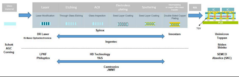
Source: Manz, Nomura research
Sales contribution to Ingentec could be significant, but cost, technical issues and resource allocation not fully resolved yet
According to our estimates, the TGV process now, with only small trial production volume, can cost USD400-500 per unit, which means the total ASP of a glass core substrate is likely over USD1,500 per unit, significantly more expensive than the large size ABF substrate of around USD200. Thus, we assume that glass core substrate ASP when entering into mass production, should be down to USD400 at least, otherwise it would not be competitive in terms of cost (Fig. 145 ).
Another issue is RDL dielectric peeling and delamination, which is currently the technology bottleneck at the substrate maker side. Once the TGV process is done, the glass core with copper pillars embedded will have to be sent to substrate makers to form the RDL to complete the overall glass core substrate production. However, the CTE (coefficient of thermal) mismatch and surface adhesion challenges between different materials including glass, ABF and copper are fundamental physics issues, not just engineering refinements. As a result, most of the substrate makers are not aggressively pushing forward the mass production of glass core substrate at the moment (Fig. 146 ).
Lastly, due to Intel’s strong commitment to the leading substrate partners such as Ibiden (4062 JP, Buy), Unimicron, and Shinko (6967 JP, NR) to bring up the EMIB-T technology into mass production, the leading substrate companies are expanding capacity for Intel aggressively through co-investment, which could put glass core substrate priority to be lower than EMIB-T. Unimicron recently announced multiple CAPEX spending on procuring equipment from Toray (3402 JP, Neutral) and ASMPT NEXX (unlisted), which we believe are mainly for EMIB-T capacity expansion. As a result, if Broadcom is really dedicated to put glass core substrate into mass production, we think it would be better for Broadcom to co-invest the capacity with its supply chain partners and provide more incentives; otherwise, itssupply chain partners may not be able to ramp up capacity smoothly considering the lack of resources and funding for glass core substrate production.
If all the issues are able to be largely resolved by the end of 2027F, we assume that there will be some revenue contribution to Ingentec by 4Q27F, with TGV ASP starting from USD200, gradually decreasing to USD140 after a few quarters. Shipments could reach hundreds of units per quarter, which could easily contribute multiple sales scale to its existing core specialty gas business (Fig. 147 ).
RDL
100%
90%
80%
70%
60%
50%
40%
30%
20%
10%
0%
nismatch circuits
~USD200
ABF)
Fig. 145: Potential BOM cost of glass core substrate vs ABF substrate
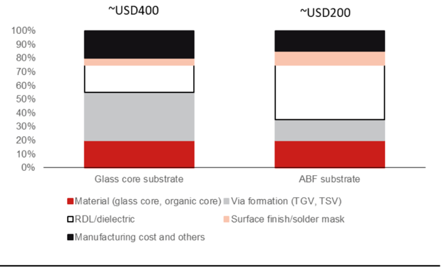
Source: Nomura estimates
Cohesive Cracking Into Glass Bulk failure
RDL Cu Trace Peeling & Seed Layer
Lift-off
Cu RDL
ABF
Cu trace
PEELING
residual tonetle stres seed Layor detaching
GLASS CORE
Residual tensile stress in electroplated copper RDL traces (due to
Cu CTE > glass CTE) causes both the seed layer and Cu trace to peel off the
ABF surface during thermal excursion or mechanical handling. This is aggravated
by low adhesion of the Ti/Cu seed to smooth glass.
ROOT: Cu residual tensile stress + poor seed adhesion
IMPACT: Open net, trace lift-off, signal
Loss
Fig. 146: RDL dielectric peeling and delamination issue on glass core substrate
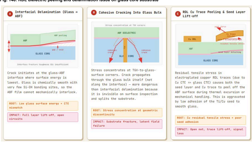
Source: Nomura research
8,000
7,000
6,000
5,000
4,000
3,000
2,000
1,000
Fig. 147: Ingentec: Sales breakdown by specialty gas and glass core substrate
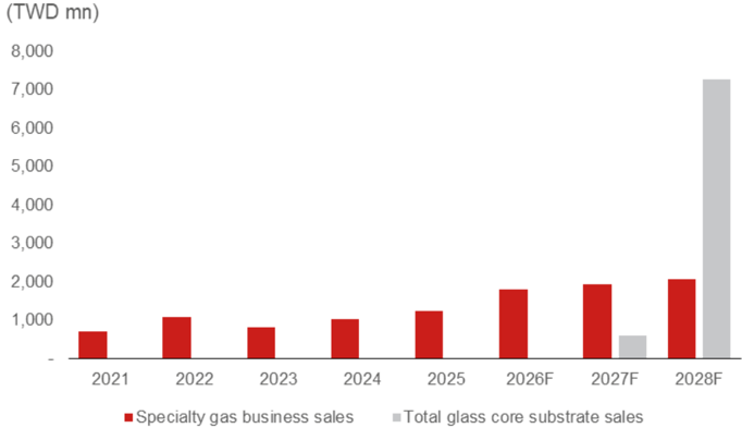
Source: Company data, Nomura estimates
Net sales
COGS
Gross profit
SG&A
1,000
800
Op income
600
Net income
EPS (TWD)
400
Profita bility
Gross margin
Op margin
200
PBT margin
Net margin
200 (%).
Sales
Gross profit
Op income
Net income
YoY (%)
Sales
Gross profit
Op profit
Net profit
Source: Bloomberg Finance L.P., Nomura estimates
1026
441
382
59
46
31
(18)
(4)
3Q25
241
180
4Q25)
648
539
104
67
61
109!
104
65
Earnings forecasts
2026F
445
379
67
56
31
(20)
(4)
4026F!
453
340 !
1027F
477
343
TWD/shr
113
54!
1,200
29 !
29
(4),
4027Fl
1.090
743
346
120 1
69
158 |
(4)!
133
57
32
44
(4)
3027F
484
329
155
58
33
64
(4)
2027F
481
337
144
58
33
54
(4)
3Q26F
448
372
76
56
31
(11)
(4)
1,000
We estimate Ingentec’s sales can grow by over 30% y-y in 2026F, driven by a recovery in the core specialty gas business. From 2027F onwards, whether glass core substrate business can take off is the most critical factor. We assume there would be some volume in 4Q27F at the earliest, with full acceleration in 2028F. However, as the company will require strong cash flow to support capex expansion, we think Ingentec may have to issue new shares or strategically work with major customers for fund-raising, and thus there could be share dilution in 2027-28F. (32) 13 1 14. 1 491 18 1 8 1.65 | 4027Fl 125 1241
(573))
(46)
(157)
| Fig. 148: Ingentec: P&L | Fig. 148: Ingentec: P&L | Fig. 148: Ingentec: P&L | Fig. 148: Ingentec: P&L | Fig. 148: Ingentec: P&L | Fig. 148: Ingentec: P&L | Fig. 148: Ingentec: P&L | Fig. 148: Ingentec: P&L | Fig. 148: Ingentec: P&L | Fig. 148: Ingentec: P&L | Fig. 148: Ingentec: P&L | Fig. 148: Ingentec: P&L | Fig. 148: Ingentec: P&L | Fig. 148: Ingentec: P&L | Fig. 148: Ingentec: P&L | Fig. 148: Ingentec: P&L | Fig. 148: Ingentec: P&L |
|---|
Source: Company data, Nomura estimates
Valuation and risks
Our TP of TWD960 is based on 60x 2028F EPS of TWD16, in the mid-range of the company’s P/E range of 45-75x over 2021-2023, when its core specialty gas business was strong, driven by tight supply due to the Ukraine-Russia war.
Downside risks include: 1) the weakening semi capex cycle; 2) a loss of market share to competitors; 3) commercialization delay in next-generation products; and 4) slower-thanexpected adoption of glass core substrate.
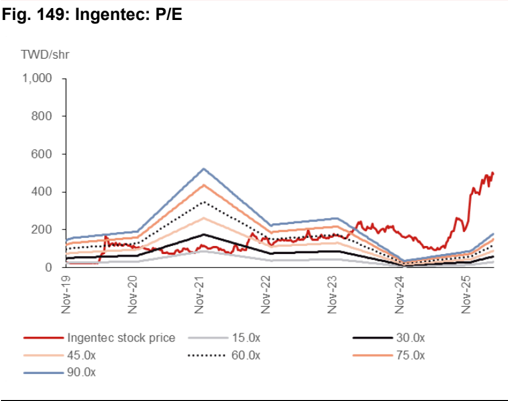
Source: Bloomberg Finance L.P., Nomura estimates
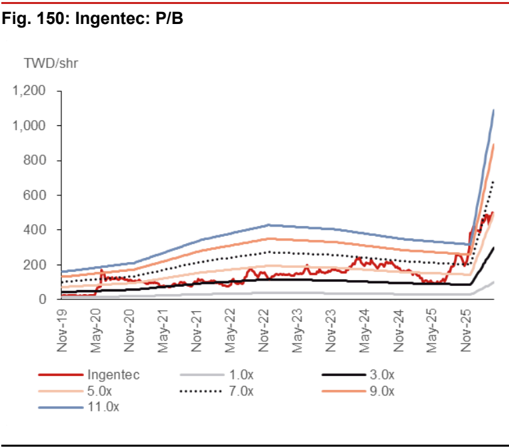
Source: Bloomberg Finance L.P., Nomura estimates
9
(44)
(363),
49
23
19
147
- 90.0x
FY24
1.017
604
413
152
79
182
9
191
37
131
2.9
FY24
40.6
17.9
18.81
12.9
FY24
FY25
1.229
927
303
170
94
39
(19)
20
19
0.4
FY25
24.6
3.2
1.6
1.5
FY25
FY26F
1,788
1,473
315
212
123
(20)
(17)
(37)
6
(24)
0.5
FY26F
17.6
-1.1
-2.1
-1.4
FY26F
1,752
779
293
167
320
(17)
303
76
246
3.9
FY27F
30.8
12.6
12.0
9.7
FY27F
Nov-25
Ticker
Semi materials
4749 TT
4768 TT
4772 TT
5234 TT
4186 JP
DD US
BAS GR
AJ FP
APD US
Mean
Median
Advanced Echem Materials
Rating
Buy
Mkt Cap
USDmn
2,917
Fig. 151: Valuation comparison table
Daxin Materials
Tokyo Ohka Kogyo
DuPont
P/E (x)
2026F
2027F
68.4
n.a
41.5
40.3
33.7
20.6
54.4
105.3
31.4
30.2
28.01
18.8
P/B (x)
2026F
2027F
9.5
13.6
10.7
9.1
5.1
1.4
8.8
2.2
8.6
n.a.
4.5
1.4
ROE (%)
2026F
2027F
14.4
(1.5)
29.5
28.2
16.0
6.7
16.8
3.2
36.2
27.2
16.5
7.0
Neutral
Not Rated
628
1,315
8.407
20.213
Current Price
(LC)
1,015.0
430.5
299.5
399.0
10.760.0
49.3
P/S (x)
2026F
2027F
17.7
11.1
11.2
7.8
4.8
2.8
14.1
7.9
8.9
8.4
4.3
2.7
EV/Sales (x)
2026F
2027F
17.5
10.4
11.5
7.6
4.8
3.2
14.0
5.2
9.1
8.1
4.3
3.1
2026F
0.8
0.9
1.7
1.9
0.8
1.6
1.0
0.7
2.3
2.8
0.9
1.7
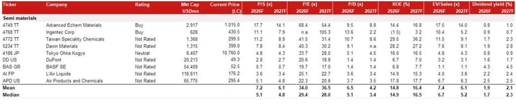
| BASF SE | 52.5 | 0.7 0.7 3.4 | 19.7 17.0 | 19.7 17.0 | 1.4 | 1.4 | 6.8 7.7 | 6.8 7.7 | 1.1 1.1 | 1.1 1.1 | 4.3 | 4.5 | 4.5 | ||
|---|---|---|---|---|---|---|---|---|---|---|---|---|---|---|---|
| L’Air Liquide | Not Rated Not Rated | 54.409 118.611 | 176.21 | 3.6 | 25.1 | 22.7 | 1.4 3.4 | 14.9 | 15.3 | 3.8 | 2.2 | 2.4 | |||
| Air Products and Chemicals | Not Rated | 65.775 | 295.4 | 5.1 4.8 | 22.3 | 20.6 | 3.6 3.7 | 3.5 | 17.8 | 17.7 | 4.0 6.7 | 6.3 | 2.5 | 2.5 | |
| 7.2 6.1 | 34.0 | 36.5 | 6.5 | 4.2 | 14.8 | 16.4 | 7.4 | 6.1 | 1.9 | 2.1 | |||||
| 5.1 4.8 | 29.4 | 28.0 | 3.4 | 14.9 | 16.5 | 6.7 | 5.2 | 1.7 | 2.3 | ||||||
| 5.1 |
Note: Bloomberg consensus for Not rated stocks; pricing as of 15 May 2026
Source: Bloomberg Finance L.P., Nomura estimates
Appendix
Company profile
Approx. Position
~14%
~4%
~4%
~3%
~1%
Ingentec Corporation is a specialty chemicals and materials manufacturer headquartered in Taiwan. Founded in 2010, the company focuses on the development, production and sales of precision chemicals and special materials for the semiconductor and optoelectronics industries. Ingentec has developed three core technology platforms: (1) Fine Chemical Distillation Technology - producing ultra-high-purity specialty gases (C4F8, SiF4, C3F8, C4F6, CH2F2, F2 mixtures) using a proprietary ‘three-cut’ distillation process with six full manufacturing steps (synthesis, purification, blending, transfilling, analysis, and special component design/assembly); (2) Vapor Etching and Decomposition Technology - patented dry etching foundry services combining equipment and recipe; and (3) Intrinsic Magnetization Filmy Thermal Conductivity Technology - producing copper magnetic wafers (CMW) with ultra-thin, high heat dissipation and magnetic permeability for advanced applications including µLED displays (TransVivi Pixel, CMuLED). Additional products include wet chemicals, TGV glass core products, tungsten ropes for crystal growth, and international trading of semiconductor/display/PCB/solar materials. In 2025, sales were approximately TWD1.23bn.
Facilities and offices
| Fig. 152: Ingentec: Facilities and offices | Fig. 152: Ingentec: Facilities and offices | Fig. 152: Ingentec: Facilities and offices | Fig. 152: Ingentec: Facilities and offices |
|---|---|---|---|
| Facility Location | Products | Use | Notes |
| Zhunan - HQ & Fab 1 | Ultra-high-purity specialty gases (C4F8, SiF4, C3F8, C4F6, CH2F2, F2 mixtures); dry etching foundry services; copper magnetic wafers (CMW); TGV glass core products | Headquarters, R&D, Manufacturing | Main production base; six full specialty gas manufacturing processes |
| Zhunan - Fab 2 | Wet chemicals (INGEST® brand); additional specialty gas and material production capacity | Manufacturing | Second production facility; capacity expansion |
| Tainan - Branch Office | - | Sales, Service | Southern Taiwan sales & customer support |
Source: Company data
Management team (Executive Committee)
Fig. 153: Ingentec: Management team
| Name | Occupation | Resume |
|---|---|---|
| Chen Ya-Li | Chairman & General Manager (CEO) | Founder of Ingentec Corporation. Established the company in 2010 and has served as Chairman and General Manager since inception. |
| Tony Chang | Director / Spokesperson | Board Director and official spokesperson of Ingentec. |
| Wang Chi-Ming | Director / Deputy Spokesperson | Board Director and Deputy Spokesperson. |
| Chiang Shou-Wei | Director | Board Director. Contributes to strategic governance and oversight. |
| Lin Hsin-Yi | Director | Board Director. |
| Shao Cheng-Te | Independent Director | Independent Director. Provides independent oversight on audit, governance and compliance matters. |
| Tseng Chuan-En | Independent Director | Independent Director. Provides independent oversight. |
Source: Company data
Major shareholders
Fig. 154: Ingentec: Shareholders
Source: Bloomberg Finance L.P.
Relative performance chart
EQUITY: TECHNOLOGY
Price
(TWD)
12001
1100-
10001
900
800-
7001
6001
140
+130
120
- 110
Advanced Echem Materials 4749.TWO 4749 TT
EQUITY: TECHNOLOGY
Courna: | CEC Namiira
Becoming TOK of Taiwan is the ultimate goal
TSMC’s major rinse supplier is aiming to further expand the market share in BARC and photoresist market
Action: Initiate coverage with a Buy rating and a TP of TWD1,500
We initiate coverage of Advanced Echem Materials (AEMC) with a Buy rating and a target price of TWD1,500, implying 48% upside. AEMC is one of the leading Taiwan-based developers and manufacturers of specialty chemical materials for semiconductor and display applications, and is among the major photoresist (PR) auxiliary domestic suppliers for a leading foundry customer. Considering the leading foundry customer’s aggressive N3/N2 and sub-2nm capacity expansion plans from 2026-27E onwards and AEMC’s potential market share gains from global peers, we forecast 2026-30F revenue/net income CAGR of around 30% for AEMC. Our TP of TWD1,500 is based on 60x FY28F EPS of TWD25 - the target multiple of 60x reflects our expectation that AEMC would sustainably grow its business with the leading foundry customer and the total addressable market (TAM) of PR would expand. The stock is currently trading at 42x 2028F EPS. Key risks include: (1) product disqualifications; (2) loss of market share; (3) a lack of new high-end products; (4) weakness in semiconductor demand.
Market share gain from global peers at leading foundry customer
AEMC’s product portfolio expansion at the leading foundry customer has mainly driven its sales. Rinse is currently the major sales contributor, where AEMC has gained market share at the leading foundry customer’s N2 node over its competitor BASF (BAS GR, NR)/3M (MMM US, NR) since 2H25. As a result, we expect AEMC’s rinse business to grow steadily along with the leading foundry customer’s capacity expansion, and its dominant position in rinse products could sustain into the A10 node based on current visibility. KrF BARC is another product that AEMC is working on to penetrate into the leading foundry customer; meanwhile, we think it might have an opportunity to challenge Du Pont’s (DD US, NR) position at the initial stage.
Taiwan’s TOK: becoming a semiconductor PR supplier is the ultimate goal
The global advanced PR market has been dominated by Japanese companies such as Tokyo Ohka Kogyo (TOK; 4186 JP, Neutral), and JSR (unlisted). Although with high technology entry barriers, we think it is a long-term call option for AEMC to be able to supply PR with great support from a leading foundry customer. On the other hand, as PR material upgrade would be required for high-NA EUV (High Numerical Aperture Extreme Ultraviolet), which is likely to further broaden the PR market, we see scope for AEMC to penetrate into the low-end PR market such as KrF PR initially.
| Year-end 31 Dec Currency (TWD) | FY25 Actual | Old | FY26F New | Old | FY27F New | Old | FY28F New |
|---|---|---|---|---|---|---|---|
| Revenue (mn) | 4,262 | 0 | 5,223 | 0 | 6,550 | 0 | 8,391 |
| Reported net profit (mn) | 1,044 | 0 | 1,372 | 0 | 1,728 | 0 | 2,298 |
| Normalised net profit (mn) | 1,044 | 0 | 1,372 | 0 | 1,728 | 0 | 2,298 |
| FD normalised EPS | 11.33 | 14.83 | 18.67 | 24.82 | |||
| FD norm. EPS growth (%) | 33.8 | 30.9 | 25.9 | 32.9 | |||
| FD normalised P/E (x) | 89.6 | - | 68.5 | - | 54.4 | - | 40.9 |
| EV/EBITDA (x) | 70.3 | - | 57.1 | - | 44.5 | - | 32.9 |
| Price/book (x) | 10.2 | - | 9.5 | - | 8.8 | - | 8.0 |
| Dividend yield (%) | 0.6 | - | 0.8 | - | 1.0 | - | 1.3 |
| ROE (%) | 17.2 | 14.4 | 16.8 | 20.5 | |||
| Net debt/equity (%) | net cash | net cash | net cash | net cash |
Source: Company data, Nomura estimates
Global Markets Research 21 May 2026
| Rating Starts at | Buy |
|---|---|
| Target price Starts at | TWD 1,500.00 |
| Closing price 15 May 2026 | TWD 1,015.00 |
| Implied upside | +47.8% |
| Market Cap (USD mn) | 2,983.5 |
| ADT (USD mn) | 89.5 |
Relative performance chart
Source: LSEG, Nomura
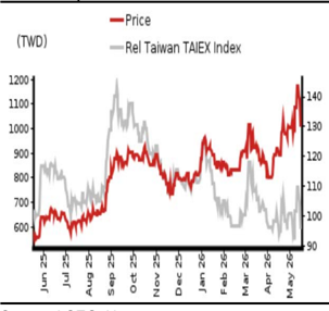
Research Analysts
Semiconductor
Donnie Teng - NIHK donnie.teng@nomura.com +852 2252 1439
Aaron Jeng, CFA - NITB
aaron.jeng@nomura.com +886(2) 21769962
Eric Chen, CFA - NITB
eric.chen@nomura.com +886(2) 21769965
Vivian Yang - NITB
vivian.yang@nomura.com +886(2) 21769970
Key data on Advanced Echem Materials
Cashflow statement (TWDmn)
| Year-end 31 Dec | FY24 | FY25 | FY26F | FY27F | FY28F |
|---|---|---|---|---|---|
| EBITDA | 819 | 1,326 | 1,632 | 2,091 | 2,814 |
| Change in working capital | -82 | -245 | -254 | -363 | -486 |
| Other operating cashflow | 207 | 35 | -97 | -197 | -351 |
| Cashflow from operations | 944 | 1,117 | 1,282 | 1,532 | 1,977 |
| Capital expenditure | -1,119 | -1,144 | -600 | -600 | -600 |
| Free cashflow | -176 | -27 | 682 | 932 | 1,377 |
| Reduction in investments | 311 | -3,032 | 212 | 212 | 212 |
| Net acquisitions | -76 | ||||
| Dec in other LT assets | -1 | 3 | -30 | 0 | |
| Inc in other LT liabilities Adjustments | 109 0 | 0 -108 | 0 -3 | 30 | 76 |
| CF after investing acts | 136 | -3,059 | 893 | 1,143 | 1,588 |
| dividends | -230 | -555 | -742 | -927 | -1,206 |
| Cash Equity issue | 5 | 5,734 | 0 | 0 | 0 |
| Debt issue | 112 | -1,530 | 0 | 0 | 0 |
| Convertible debt issue | 0 | 0 | 0 | 0 | 0 |
| Others | -9 | -88 | -88 | -88 | -88 |
| acts | -830 | -1,016 | |||
| CF from financial | -122 | 3,560 | 128 | -1,294 | |
| Net cashflow | 14 | 501 | 63 | 294 | |
| Beginning cash | 423 | 437 | 938 | 1,001 | 1,128 |
| Ending cash | 437 | 938 | 1,001 | 1,128 | 1,423 |
| Ending net debt | -1,423 | ||||
| 1,081 | -938 | -1,001 | -1,128 | ||
| Balance sheet (TWDmn) As at 31 Dec | FY24 | FY26F | FY27F | FY28F | |
| Cash & equivalents | 437 13 | FY25 938 2,942 | 1,001 2,942 676 | 1,128 2,942 847 | 1,423 2,942 1,085 |
| Marketable securities Accounts receivable | 532 | 551 | |||
| Inventories | 677 | 904 | 1,097 | 1,383 | 1,754 |
| Other current | 157 | 147 | 147 | 147 | 147 |
| assets | 7,351 | ||||
| Total current assets | 1,815 | 5,481 | 5,862 | 6,448 713 | 713 |
| LT investments | 218 | 713 | 713 | ||
| Fixed assets | |||||
| Goodwill | 2,770 | 3,743 | 4,060 | 4,340 | 4,576 |
| 635 | |||||
| Other intangible assets Other LT assets Total assets | 531 5,334 180 197 | 532 10,469 0 300 | 529 11,164 0 | 559 12,060 0 459 | 13,276 0 |
| Short-term debt Accounts payable Other current | 667 | 364 667 | 667 | 583 | |
| liabilities Total current liabilities | 779 | 967 | 667 | ||
| 1,126 | 1,249 | ||||
| Long-term debt | 1,156 1,102 | 0 | 1,031 0 | 0 | 0 |
| Convertible debt | 142 | 251 | 251 | 251 | |
| Other LT liabilities Total liabilities | 2,400 | 251 | 1,377 10 | 10 | |
| Minority interest | 1,217 | 1,282 10 | 1,500 | ||
| Preferred stock | 10 | 10 | 7,501 | 7,501 | |
| Common stock Retained earnings | 1,723 1,174 | 7,501 1,663 | 7,501 2,294 | ||
| Proposed dividends | 3,095 | 4,187 | |||
| Other equity and reserves | 28 | 78 | 78 | 78 10,674 | 78 |
| Total shareholders’ | 2,925 | 9,242 | 9,873 11,164 | 11,766 | |
| equity Total equity & liabilities | 5,334 | 13,276 | |||
| 10,469 | 12,060 | ||||
| Liquidity (x) Current ratio Interest cover | 1.57 36.6 | 5.67 - cash | 5.69 - net cash net cash | 5.73 - net | 5.88 - net |
| Leverage Net debt/EBITDA (x) Net debt/equity (%) | 1.32 | net cash | net cash cash | net cash | |
| Per share | 36.9 | cash | |||
| Reported EPS (TWD) | net | ||||
| Norm EPS (TWD) | 8.47 8.47 | 11.33 11.33 11.33 | 14.83 14.83 14.83 | 18.67 18.67 18.67 | 24.82 24.82 24.82 |
| FD norm EPS (TWD) BVPS (TWD) DPS (TWD) | 8.47 35.55 2.79 | 99.85 6.00 | 106.66 8.01 | 115.32 10.02 | 127.11 13.02 |
| Activity (days) | |||||
| 58.5 | 46.4 | 42.9 | 42.4 | 42.1 | |
| Days receivable | 121.9 | ||||
| Days inventory | 116.7 | 118.9 | 123.9 | 121.9 | |
| 34.0 | 37.4 | 41.2 | |||
| Days payable | 40.5 | 40.5 | |||
| 141.2 | 127.9 | 125.6 | 123.6 | ||
| Cash cycle | 123.8 |
Source: Company data, Nomura estimates
Performance
| (%) | 1M | 3M | 12M | ||
|---|---|---|---|---|---|
| Absolute (TWD) | 11.4 | 22.3 | 83.9 | M cap (USDmn) | 2,983.5 |
| Absolute (USD) | 11.7 | 21.8 | 75.6 | Free float (%) | 78.8 |
| Rel to Taiwan TAIEX Index | -0.7 | -0.2 | -5.6 | 3-mth ADT (USDmn) | 89.5 |
Income statement (TWDmn)
| Year-end 31 Dec | FY24 | FY25 | FY26F | FY27F | FY28F |
|---|---|---|---|---|---|
| Revenue | 3,322 | 4,262 | 5,223 | 6,550 | 8,391 |
| Cost of goods sold | -2,117 | -2,426 | -2,946 | -3,715 | -4,711 |
| Gross profit | 1,204 | 1,835 | 2,277 | 2,835 | 3,680 |
| SG&A | -618 | -774 | -938 | -1,073 | -1,241 |
| Employee share expense | |||||
| Operating profit | 587 | 1,062 | 1,339 | 1,762 | 2,440 |
| EBITDA | 819 | 1,326 | 1,632 | 2,091 | 2,814 |
| Depreciation | -225 | -255 | -283 | -319 | -364 |
| Amortisation | -7 | -10 | -10 | -10 | -10 |
| EBIT | 587 | 1,062 | 1,339 | 1,762 | 2,440 |
| Net interest expense | -16 | 53 | 56 | 56 | 56 |
| Associates & JCEs | |||||
| Other income | 258 | 145 | 239 | 240 | 240 |
| Earnings before tax | 828 | 1,259 | 1,634 | 2,058 | 2,736 |
| Income tax | -131 | -215 | -261 | -329 | -438 |
| Net profit after tax | 697 | 1,044 | 1,373 | 1,729 | 2,298 |
| Minority interests | 0 | 0 | 0 | 0 | 0 |
| Other items | |||||
| Preferred dividends | |||||
| Normalised NPAT | 697 | 1,044 | 1,372 | 1,728 | 2,298 |
| Extraordinary items | |||||
| Reported NPAT | 697 | 1,044 | 1,372 | 1,728 | 2,298 |
| Dividends | -230 | -555 | -742 | -927 | -1,206 |
| Transfer to reserves | 467 | 488 | 630 | 801 | 1,092 |
| Valuations and ratios | |||||
| Reported P/E (x) | 119.9 | 89.6 | 68.5 | 54.4 | 40.9 |
| Normalised P/E (x) | 119.9 | 89.6 | 68.5 | 54.4 | 40.9 |
| FD normalised P/E (x) | 119.9 | 89.6 | 68.5 | 54.4 | 40.9 |
| Dividend yield (%) | 0.3 | 0.6 | 0.8 | 1.0 | 1.3 |
| Price/cashflow (x) | 88.5 | 83.8 | 73.3 | 61.3 | 47.5 |
| Price/book (x) | 28.6 | 10.2 | 9.5 | 8.8 | 8.0 |
| EV/EBITDA (x) | 116.0 | 70.3 | 57.1 | 44.5 | 32.9 |
| EV/EBIT (x) | 161.9 | 87.8 | 69.6 | 52.8 | 38.0 |
| Gross margin (%) | 36.3 | 43.1 | 43.6 | 43.3 | 43.9 |
| EBITDA margin (%) | 24.6 | 31.1 | 31.2 | 31.9 | 33.5 |
| EBIT margin (%) | 17.7 | 24.9 | 25.6 | 26.9 | 29.1 |
| Net margin (%) | 21.0 | 24.5 | 26.3 | 26.4 | 27.4 |
| Effective tax rate (%) | 15.8 | 17.1 | 16.0 | 16.0 | 16.0 |
| Dividend payout (%) | 33.0 | 53.2 | 54.1 | 53.7 | 52.5 |
| ROE (%) | 26.0 | 17.2 | 14.4 | 16.8 | 20.5 |
| ROA (pretax %) | 13.2 | 14.7 | 13.6 | 16.7 | 21.4 |
| Growth (%) | |||||
| Revenue | 40.5 | 28.3 | 22.6 | 25.4 | 28.1 |
| EBITDA | 94.8 | 62.0 | 23.1 | 28.1 | 34.6 |
| Normalised EPS | 8.5 | 33.8 | 30.9 | 25.9 | 32.9 |
| Normalised FDEPS | 8.5 | 33.8 | 30.9 | 25.9 | 32.9 |
Source: Company data, Nomura estimates
Company profile
AEMC was founded in 2003 and committed to the development and manufacturing of specialized chemical materials, mainly photoresist auxiliary for “semiconductor and display” applications. In 2020, it has started to expand R&D facility in Taoyuan, and gradually established two factories for production of semiconductor materials in Tainan and Kaohsiung (Southern Taiwan Science Park).
Valuation Methodology
Our TP TWD1,500 is based on 60x FY28F EPS TWD25, in the mid-range of its historical P/E of 30-80x to address the stably growing business with the leading foundry customer as well as the rising total addressable market (TAM) of photoresist and photoresist auxiliary. The bench mark market index is TAIEX.
Risks that may impede the achievement of the target price
Downside risks include: 1) products are disqualified by the leading foundry customer; 2) losing market share to other competitors; 3) not able to supply more high-end products such as BARC and photoresist; 4) the weakening Semi market demand.
ESG
AEMC publishes sustainability report every year. Its goal is continuous innovation in green product design refers to the continuous search for new and environmentally friendly solutions when designing products to reduce the negative impact on the environment while improving the quality and efficiency of products.
Photoresist and photoresist auxiliary
Photoresist (PR) introduction
PR is a light-sensitive polymer used for wafer photolithography in IC manufacturing. The photolithography process is the most time-consuming step in the whole IC manufacturing process. During the photolithography process, PR is applied on the wafer surface before the etch process, and then it is allowed to be dissolved away once the etching process is over. There are two purposes behind the application of PR layers: (1) to form precise patterns, and (2) to protect the substrate from being damaged by chemicals during the etching process.
PR is the key material for photolithography, and in manufacturing, the quality has a substantial impact on its performance. PRs are usually composed of adhesive agents (~20%), sensitizers (~10%) and solvents (~70%). A good PR usually requires high contrast, high resolution and high sensitivity, so that the circuit pattern can be copied precisely to the wafer surface. What is more, high purity, strong etch resistance, dissolvability, and a defined surface tension, density and viscosity are also essential for good PR, due to the manufacturing engineering standards.
The global PR market has been dominated by companies from Japan for a long time such as Tokyo Ohka Kogyo (TOK; 4186 JP, Neutral), and JSR (unlisted).
In terms of different reactions when exposed to UV light, there are two types of semiconductor PR: positive PR and negative PR (Fig. 156 ).
- With positive PR, UV light strategically hits the material in the areas that need to be removed. These exposed areas are then washed away by PR developer solvent, leaving the underlying material. The areas of the PR that are not exposed to the UV light are left insoluble to the PR developer. As a result, there is an identical copy of the pattern that exposed as a mask on the wafer. ·
- Negative PR, which is just the opposite of positive PR, is extremely difficult to dissolve. The UV exposed negative resist remains on the wafer while the PR developer solution works to remove the areas that are unexposed. This leaves a mask that consists of an inverse pattern of the original, which is applied on the wafer. ·
Both positive and negative PRs are used in the semiconductor manufacturing industry, but more suppliers opt for positive PR due to higher resolution and higher-resolution capabilities.
PR auxiliary introduction
- BARC (Bottom Anti-Reflective Coatings; Film) ·
BARC is placed beneath the PR layer to prevent light reflection from the substrate. This helps to suppress standing waves caused by interference within the resist layer during exposure, which can lead to variations in sidewall profiles and critical dimensions. As a result, BARC improves the accuracy of lithography.
- EBR (Edge Bead Removal) ·
EBR is a process that removes excess PR from the edge of a coated substrate preventing defects that may arise due to non-uniformity. EBR materials are the specialized solvent mixtures designed to dissolve and remove excess PR.
- Developer ·
Developer is a chemical agent used in photolithography to dissolve and remove soluble portions of PR, revealing the underlying circuit pattern.
- Rinse ·
Rinse materials are specialized chemical solutions, often containing surfactants or, in the case of Dry Development Rinse (DDR), functional polymers, used after PR development in lithography to prevent pattern collapse.
BARC (thinfilm)
photoresist
EBR
PR removal ·
- Substrate clean
Thin film
Light source
Photomask -
PR removal involves stripping, ashing, or cleaning PR polymers after lithography using chemical solvents (Acetone, NMP, DMSO), plasma ashing, or wet cleaning (SPM).
Fig. 155: PR and lithography process
Developer
Rinse
Photoresist solvent
Oxide film
Wafer photoresist is removed to reveal the patterns.
UV light
Source: Nikon, Nomura research
Fig. 156: PR processes and the materials required

Source: Nomura research
Method of stepper
Lens in illumination
system
Silicon substrate
Exposing
Low
Photoresist
Fig. 157: The technology difficulties of PR and auxiliaries
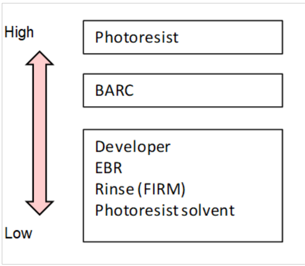
Source: Nomura research
0.33 NA EUV
0.55 NA EUV
The change of PR and related materials are required for high-NA EUV
With a higher NA, photons strike the wafer at a shallower angle. That requires thinner PR layers to avoid shadowing. The upside is that a thinner resist layer reduces the risk of pattern collapse, as the aspect ratio of resist features is smaller. However, it also provides less protection for the wafer. In addition, long etch processes used to create high-aspect ratio wafer features can erode the resist layer, ultimately degrading the transferred pattern. With less material a thinner resist also captures fewer photons, potentially making roughness and other stochastic effects worse.
At present, metal-oxide resists are probably the leading alternative to photoacid-driven chemistries, or chemically amplified resists (CAR). Based on a metal-oxide core, surrounded by ligands that tune solubility, crosslinking, and other properties, these resists offer inherently good etch resistance. The dense core absorbs more energy, too, attenuating electron energy and reducing blur. Due to the change of materials, the PR price for high-NA EUV could be much higher than the existing EUV. According to our industry survey, the PR for high-NA EUV can be up to USD10,000-40,000 per gallon, increase significantly from USD5,000 for existing EUV.
Improved etch resistance and absorption address the most serious limitations of thin resists, offering a high NA-friendly solution. Unfortunately, only negative tone metal-oxide resists are available, so they cannot be used for contact holes. Both Inpria (unlisted; acquired by JSR [unlisted]) and Lam Research (LRCX US, NR) offer metal-oxide resists, differentiated in part by their approaches to development. Lam Research is attempting to disrupt the whole stack. Instead of a wet PR technology using a spin coater, they will use a chemical vapor deposition process to layer on a metal PR. The throughput and patterned lines would be slower but more accurate. If using TEL and JSR’s solution, due to the change of the material of PR, the developer would need to be changed as well. Currently, Tetramethylammonium Hydroxide (TMAH) is widely used as developer for existing EUV. But for high-NA EUV, propylene glycol methyl ether acetate (PGMEA) with acid is likely a better solution. We expect TOK is likely the major supplier. The purity requirement of developer would be higher as well.
Although the existing wet process solution supplied by TEL and JSR will be likely more cost effective without procuring the new equipment, we expect TSMC (2330 TT, Buy) to adopt Lam Research’s solution in the high-NA EUV era.
Fig. 158: The reduction in PR film thickness
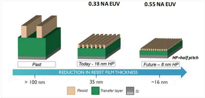
Source: Cadence
Lam nesearch is usiiig aly deposition and aly develop equipment to growelmindle rh
4X more photons absorbed / volume
building blocks
45000
40000
Wet photoresist application - adding up photoresist
35000
30000
25000
Exposure - EUV
20000
15000
Wet developing - washing out the photoresist by using solvant
10000
5000
Etching
0
>>10X higher etch selectivity & contrast
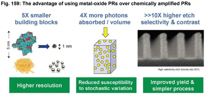
Source: Inperia
High-NA
Fig. 160: The price of PR per gallon
Although MOR carries higher ASP, the usage is much smaller than regular high-NA EUV ph
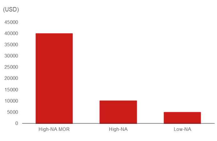
Source: Nomura estimates
Fig. 161: TEL and JSR vs Lam Research’s solution
Lam Research is using dry deposition and dry develop equipment to grow/eliminate PR
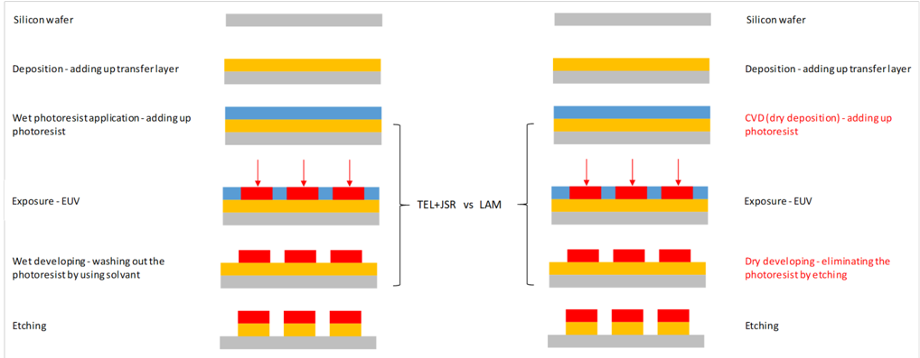
Source: TEL, Lam Research, Nomura research
LOW-NA
Silicon wafer
Deposition - adding up transfer layer
CVD (dry deposition) - adding up photoresist
Exposure - EUV
Dry developing-eliminating the photoresist by etching
Etching
ASP (USD per gallon)
Nodes (nm)
Suppliers
Note
‹100
100-1000
ArF
1000-1500
EUV
1000-5000
High-NA EUV
5000
Fig. 162: The spec of different PRs by nodes and major suppliers
High-NA MOR (metal oxide resist)
10000
>40000 (but with low throughput)
13.5 (with 0.55 NA)
⇐1nm
| TOK | Shin-etsu | Shin-ets u | Shin-etsu TOK | Entegris | Entegris |
|---|---|---|---|---|---|
| Dow | JSR | TOK | JSR Shin-etsu | Gelest (Nanomate) | |
| Merck | Dow | Sumitomo | |||
| Fujifilm | Fujifilm | ||||
| TOK is the | TOK is the | ||||
| Market share consolidation to winner of EUV | | Market share consolidation to winner of EUV | | JSR could regain share in high-NA EUV technology could outpace Tokyo Electronc’s track technoloy | |||
| photoresist | photoresist | 2. Entegris and Gelest (through | |||
| market used on; | market used on; | Nanomate in Taiwan) could be the | |||
| 1-2nm nodes | 1-2nm nodes | new photo resist suppliers |
Source: Nomura research and estimates (for high-NA EUV related information)
JSR
JSR
Countries
9,000
8,000
7,000
6,000
Taiwan
5,000
4,000
3,000
2,000
1,000
China
Japan
Us
Germany
France
Korea
Companies
Tickers
G-line/t line
High-NA
MOR
Precursor Lithograp
Photoresist auxiliary
(USD mn)
Developer
EBR
Rinse
1000
Cleaner /Depositi on
hy
AEMC is expanding market share in PR auxiliary market and aiming to produce PR
Specialty gas
Etching
Doping dw
AEMC has been expanding its market share at the leading foundry customer, including rinse and cleaner. Rinse is currently the major sales contributor for AEMC, where AEMC has gained significant market share at the leading foundry customer’s N2 node over its competitor BASF/3M since 2H25. As a result, we expect AEMC’s rinse business to grow steadily along with the leading foundry customer’s capacity expansion, and its dominant position in rinse products could sustain to the A10 node based on current visibility. KrF BARC is another product that AEMC is working on to penetrate into the leading foundry customer, while we think it has a likelihood to challenge Du Pont’s position at the initial stage. Compared with the distant PR material market leader TOK. AEMC’s sales CAGR was 23% in 2020-2025 vs TOK’s CAGR of 9% (only include TOK’s electronic functional materials business). Under the leading foundry’s localization plan, if AEMC can execute well to further improve its technology capability, we expect AEMC to further increase the market share in the long term.
Saesol Diamond unlisted
Fig. 163: The matrix of some key Semi materials vs suppliers
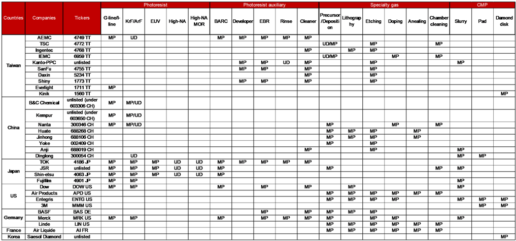
Source: Company data, Nomura research
Fig. 164: AEMC: sales breakdown by product lines
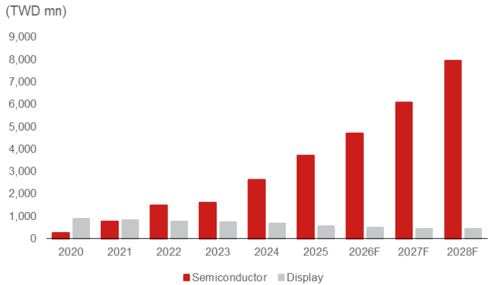
Source: Company data, Nomura estimates
KrF/ArF
Photoresist
EUV
High-NA
BARC
Anealing
Chamber cleaning
Slurry dW
2023
_ AEMC
2024
CMP
Pad
2025
— AEMC/TOK ratio
$ 3
Fig. 165: AEMC sales vs TOK EFM sales
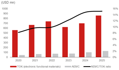
Source: Company data Note: EFM: electronic functional materials
Damond disk
16%
14%
12%
10%
8%
6%
4%
2%
0%
Net sales
COGS
Gross profit
SG&A
Op income
Net income
EPS (TWD)
Gross margin
Op margin
PBT margin
Net margin
Qo0 (%)
Sales
Gross profit
Op income
Net income
YoY (%)
Sales
Gross profit
Op profit
Net profit
585
620
3Q25
1,066
615
4Q25!
1,084 i
607
375
533
450
477 1
Earnings forecast
2Q27F
1,525
859
666
122
120
424
74
3Q27F
1,758
994
764
135
130
499
74
2026F
1,296
740
557
109
113
335
74
3Q26F
1,337
761
576
111
115
350
74
4026Fl
1,344 i
766
579 1
1281
134;
74!
1027F
1,500
849
651
120
127
403
74
1Q26
1,246
680
566
112
117
337
73
In 2026F, AEMC is facing capacity constraints due to phase 1 of its major production facility in Kaohsiung reaching the capacity limit. The company is expecting phase 2 capacity to be qualified by customers by the end of 2026F at the earliest. The phase two capacity can support another TWD5bn sales from current annual run rate of TWD5bn sales in 2026F. As a result, we expect AEMC’s sales could grow over 20% continuously in 2026-2029F to reach TWD10bn levels.
Fig. 166: AEMC: P&L
2027F
2
5
3027F
15
15
18
4027F!
1,767 1
1,012!
754
155
163
436 |
74
510 l
82
429 1
42.7
24.71
28.9l
24.31
4027F
(1)|
(12)|
2026F
4
(2)
(1)
3171
4Q26FH
11
(10)!
1027F
12
12
27
(8)
(15)
(27)
21
6
(2)
15
19
33
| 20 | 37 | 2 | 29 | 4 | 22 | 4 | 15 | (11)} | |||||||
|---|---|---|---|---|---|---|---|---|---|---|---|---|---|---|---|
| 1Q25 | 4027Fl | ||||||||||||||
| 2025 | 3Q25 24 | 4Q25 | 1026 | 2026F 12 | 3Q26F | 4026Fl | 1Q27F | 2Q27F | 3Q27F | 31 | FY24 | FY25 28 | FY26F 23 | FY27F | |
| 39 81| | 34 63 | 40 | 18 37 1 | 30 51 | 25 28 | 24 H 211 | 20 15 | 18 20 | 32 33 | 30 | 52 | 24 | 25 25 | ||
| 86 | 56 | 76 | 25 | 20 | 38 | 81 | 32 | ||||||||
| 117 | 45 | 81 | (6) | 35 | 26 | 42 | 26 | ||||||||
| 20 | 87 | 51 l | 63 | 21 | 25 | 18 | 22 | 35 | 31 | 50 | 31 | 26 |
(10))
Source: Company data, Nomura estimates
3026F
3
3
FY24
3,322
2,117
1,204
339
279
587
242
828
131
697
8.5
FY24
36.3
17.7
24.9
21.0
FY24
FY25
4,262
2,426
1,835
388
385
1,062
198
1,259
215
1,044
11.3
FY25
43.1
24.9
29.5
24.5
FY25
FY26F
5,223
2,946
2,277
459
479
1,339
295
1,634
267
1,367
14.7
FY26F
43.6
25.6
31.3
26.2
FY26F
3,715
2,835
533
541
1,762
296
2,058
329
1,729
18.6
FY27F
43.3
26.9
31.4
26.4
FY27F
Ticker
Semi materials
4749 TT
4768 TT
1,400
4772 TT
5234 TT
1,200
4186 JP
DD US
1,000
BAS GR
AJ FP
800
APD US
Mean
600
Median
400
Rating
Buy
Advanced Echem Materials
Mkt Cap
USDmn
2.917
Valuation and risks
628
1.368
1,315
8.407
Current Price
(LC)
1.015.0
430.5
299.5l
399.0
10.760.0|
P/S (x)
2026F
17.7
11.1
11.2
7.8
4.8
P/E (x)
2027F|
TWD/shr
2026F
14.1
68.4
7.9
1,400
8.9
8.4
1,200
4.3
n.a
41.5
40.3
33.7
2027F
54.4
105.3
31.4
30.2
28.0
P/B (x)
2026F
9.5
13.6
10.7
9.1
5.1
2027F
8.8
2.2
8.6
n.a.
4.5
ROE (%)
2026F
2027F
14.4
(1.5)
29.5
28.2
16.0l
Our TP of TWD1,500 is based on 60x FY28F EPS TWD25, in the mid-range of its historical P/E of 30-80x, given our expectation that AEMC would sustainably grow its business with the leading foundry customer as well as the total addressable market (TAM) of photoresist and photoresist auxiliary would rise. 400 1.4 14 6.7 6.8 14.9
200
Downside risks include: (1) product disqualifications by the leading foundry customer; (2) loss of market share to other competitors; (3) not being able to supply more high-end products such as BARC and photoresist.
… 60.0x
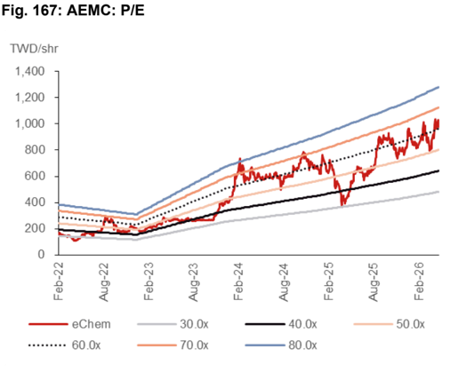
Source: Bloomberg, Nomura estimates
Fig. 169: Valuation comparison
Note: Bloomberg consensus for Not rated stocks; pricing as of 15 May 2026Source: Bloomberg Finance L.P., Nomura estimates
Aug-24
EV/Sales (x)
2026F
2027F
17.5
10.4
11.5
7.6
4.8
3.2
1.1
4.0
6.7
7.4
6.7
14.0
5.2
9.1
8.1
4.3
3.1
1.1
3.8
6.3
6.1
5.2
Feb-25
2026F
0.8
0.9
1.7
1.9
0.8
1.6
4.3
2.2
2.5
1.9
1.7
Aug-25
1.0
0.7
2.3
2.8
0.9
1.7
4.5
2.4
2.5
2.11
2.3
Feb-26
Feb-24
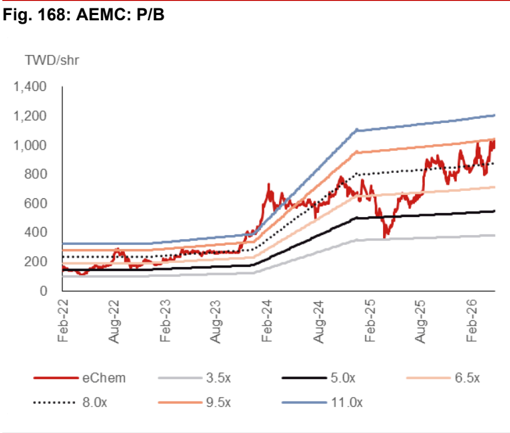
Source: Bloomberg, Nomura estimates
16.8
3.2
36.2
27.2
16.5
7.0
7.7
15.3
17.7
16.4
16.5
IC manufacturing materials, cleaning chemicals,
Appendix
Company profile
Use
Headquarters, R&D, Manufacturing
Manufacturing
Advanced Echem Materials Company Limited (AEMC) is a specialty chemicals company focused on the development and manufacturing of electronic materials for semiconductor advanced processes, advanced packaging, and display applications. Founded in 2003 and headquartered in Longtan District, Taoyuan City, Taiwan, AEMC’s products include IC manufacturing materials, cleaning chemicals, CMOS image sensor materials, fingerprint-on-display sensor materials, chip-on-film materials, packaging materials, TFT PR, resin black matrix, and micro-LED materials. The company invests more than 10% of its annual revenue in R&D and maintains a chemical R&D team that accounts for approximately one-third of its headcount. AEMC has received support from nine government science and technology programs and holds multiple patents. In 2025, revenue was approximately TWD4.3bn.
Facilities and offices
Fig. 170: AEMC: facilities and offices
Source: Company data
Management team (Executive Committee)
Fig. 171: AEMC: management team
| Name | Occupation | Resume |
|---|---|---|
| Yang Chih-Sheng | Chairman & General Manager | Founder and Chairman of AEMC since its establishment in 2003. Also serves as General Manager, overseeing both strategic direction and daily operations. Under his leadership, AEMC has grown from a startup into a leading supplier of specialty electronic chemicals for the semiconductor and display industries in Taiwan and internationally. |
| Li Tsung-Jung | Director | Board member of AEMC. Contributes to corporate governance and strategic oversight. |
| Chang Chiu-Huang | Director | Board member of AEMC. |
| Pu Sheng-Ming | Director (Rep. of Yanwen Asset Management) | Board member representing Yanwen Asset Management Consulting Co., Ltd. |
| Cheng Chung-Jen | Independent Director | Independent board member providing oversight on corporate governance and compliance. |
| Liu Chih-Hung | Independent Director | Independent board member. |
| Sharen Lu | Director of Administration / Spokesperson | Serves as AEMC’s official spokesperson and heads the administration function. Main point of contact for investor relations. |
Source: Company data
Notes
Main R&D and production base
Established 2020;
production facility near
Southern Taiwan Science
Park
Established 2020;
expanding capacity
Major shareholders
Fig. 172: AEMC: shareholders
Fubon Elite Mid-Small Cap Fund
Approx. position
~15%
~5%
~5%
~5%
| Fubon Taiwan Sustainable Growth Dividend Fund |
|---|
Source: Bloomberg Finance L.P.
Relative performance chart
EQUITY: TECHNOLOGY
Price
(TWD)
6001
5001
400-
300-
-115
- 110|
• 105
• 100
• 95
Kinik Company 1560.TW 1560 TT
EQUITY: TECHNOLOGY
Courca. I CEC Namura
Critical CMP and reclaim wafer role player
Riding on the growing demand for CMP and reclaim wafer; grinding wheel could be additional catalyst
Action: Initiate coverage with Buy rating and TWD840 TP
Kinik is the dominant chemical mechanical polishing (CMP) pad conditioner (DBU) supplier to the leading foundry with ~80% share on the N2 node through a multi-year co-development partnership. Kinik’s reclaim/test wafer business (SBU) is also likely growing along with the recovery of semi wafer demand. Other than these two growth engines, we expect its grinding wheel business (ABU) could be an additional lever if Kinik is able to penetrate into the leading OSAT companies in the long term. We initiate coverage of Kinik with a Buy rating and a TP of TWD840, based on 40x 2028E EPS TWD21, in the upper half of its historical P/E of 10-45x, to address its stably growing business with the leading foundry customer as well as the rising total addressable market (TAM) across its different business units. The stock is trading at 31x 2028F EPS. We expect Kinik’s sales/net profit to see a 21%/75% CAGR in 2026-28F. Risks include: 1) products no passing qualification; 2) losing market share; 3) failure to broaden the product portfolio; and 4) weakening semi market demand.
DBU and SBU are set to see secular growth in 2026-28F
Kinik has secured the leading position as the major CMP pad conditioner supplier to the leading foundry customer since the N3 node over its peer 3M (MMM US, Not rated). As the A16 node will initially adopt backside power (BPD) technology with 20-30% more CMP processes required, we expect DBU sales growth to be secured. Also, Kinik’s Intel business looks to be improving, as Intel is ramping up its A18 node production. For SBU business, as the upcoming Backside Power Delivery (BPD) and wafer-bonded NAND semi technologies will consume more wafers, we expect it would be also a positive catalyst for reclaim/testing wafer demand. DBU and SBU combined may account for more than 70% of Kinik’s total sales in 2026F, in our view.
Expanding the ABU business into semi market is the ultimate goal
Currently, Kinik’s ABU business is mainly for industrial and automation applications rather than semi. Management is aiming to expand the ABU business into the semi market, such as working closely with major OSAT companies to address wafer-grinding opportunities. According to our estimates, the semi wafer grinding wheel market is as big as that for CMP pad conditioner - both USD400mn+ in 2025. Disco (6146 JP, Neutral) is the distant leader in the semi wafer grinding wheel market.
| Year-end 31 Dec Currency (TWD) | FY25 Actual | Old | FY26F New | Old | FY27F New | Old | FY28F New |
|---|---|---|---|---|---|---|---|
| Revenue (mn) | 8,149 | 0 | 9,702 | 0 | 11,353 | 0 | 14,200 |
| Reported net profit (mn) | 1,360 | 0 | 1,982 | 0 | 2,439 | 0 | 3,020 |
| Normalised net profit (mn) | 1,360 | 0 | 1,982 | 0 | 2,439 | 0 | 3,020 |
| FD normalised EPS | 9.33 | 13.60 | 16.73 | 20.72 | |||
| FD norm. EPS growth (%) | 31.4 | 45.7 | 23.1 | 23.8 | |||
| FD normalised P/E (x) | 68.8 | - | 47.2 | - | 38.4 | - | 31.0 |
| EV/EBITDA (x) | 48.4 | - | 33.3 | - | 26.8 | - | 21.2 |
| Price/book (x) | 11.5 | - | 10.1 | - | 8.5 | - | 7.1 |
| Dividend yield (%) | 0.6 | - | 0.8 | - | 0.8 | - | 0.8 |
| ROE (%) | 17.8 | 22.8 | 24.2 | 25.0 | |||
| Net debt/equity (%) | net cash | net cash | net cash | net cash |
Source: Company data, Nomura estimates
Global Markets Research 21 May 2026
| Rating Starts at | Buy |
|---|---|
| Target price Starts at | TWD 840.00 |
| Closing price 15 May 2026 | TWD 642.00 |
| Implied upside | +30.8% |
| Market Cap (USD mn) ADT (USD mn) | 2,997.4 |
| 49.2 |
Relative performance chart
Source: LSEG, Nomura
Research Analysts
Semiconductor
Donnie Teng - NIHK donnie.teng@nomura.com +852 2252 1439
Aaron Jeng, CFA - NITB
aaron.jeng@nomura.com +886(2) 21769962
Eric Chen, CFA - NITB
eric.chen@nomura.com +886(2) 21769965
Vivian Yang - NITB
vivian.yang@nomura.com +886(2) 21769970
Key data on Kinik Company
Performance
| (%) | 1M | 3M | 12M | ||
|---|---|---|---|---|---|
| Absolute (TWD) | 23.2 | 51.1 | 117.6 | M cap (USDmn) | 2,997.4 |
| Absolute (USD) | 23.5 | 50.4 | 107.9 | Free float (%) | 74.7 |
| Rel to Taiwan TAIEX Index | 11.1 | 28.5 | 28.2 | 3-mth ADT (USDmn) | 49.2 |
Income statement (TWDmn)
| Year-end 31 Dec | FY24 | FY25 | FY26F | FY27F | FY28F |
|---|---|---|---|---|---|
| Revenue | 7,019 | 8,149 | 9,702 | 11,353 | 14,200 |
| Cost of goods sold | -4,831 | -5,502 | -6,135 | -7,055 | -8,907 |
| Gross profit | 2,188 | 2,647 | 3,568 | 4,298 | 5,294 |
| SG&A | -1,033 | -1,344 | -1,482 | -1,645 | -1,913 |
| Employee share expense | |||||
| Operating profit | 1,155 | 1,303 | 2,086 | 2,653 | 3,380 |
| EBITDA | 1,164 | 1,955 | 2,799 | 3,426 | 4,249 |
| Depreciation | -9 | -642 | -703 | -763 | -858 |
| Amortisation | 0 | -10 | -10 | -10 | -10 |
| EBIT | 1,155 | 1,303 | 2,086 | 2,653 | 3,380 |
| Net interest expense | 18 | 1 | -1 | -1 | -1 |
| Associates & JCEs | |||||
| Other income | 115 | 354 | 388 | 400 | 400 |
| Earnings before tax | 1,289 | 1,658 | 2,473 | 3,052 | 3,780 |
| Income tax | -227 | -263 | -439 | -549 | -680 |
| Net profit after tax | 1,062 | 1,395 | 2,034 | 2,502 | 3,099 |
| Minority interests | -27 | -35 | -52 | -64 | -79 |
| Other items | |||||
| Preferred dividends | |||||
| Normalised NPAT | 1,035 | 1,360 | 1,982 | 2,439 | 3,020 |
| Extraordinary items | |||||
| Reported NPAT | 1,035 | 1,360 | 1,982 | 2,439 | 3,020 |
| Dividends | -640 | -584 | -729 | -729 | -729 |
| Transfer to reserves | 395 | 776 | 1,253 | 1,710 | 2,292 |
| Valuations and ratios | |||||
| Reported P/E (x) | 90.4 | 68.8 | 47.2 | 38.4 | 31.0 |
| Normalised P/E (x) | 90.4 | 68.8 | 47.2 | 38.4 | 31.0 |
| FD normalised P/E (x) | 90.4 | 68.8 | 47.2 | 38.4 | 31.0 |
| Dividend yield (%) | 0.7 | 0.6 | 0.8 | 0.8 | 0.8 |
| Price/cashflow (x) | 57.9 | 48.9 | 28.7 | 25.6 | 23.0 |
| Price/book (x) | 13.1 | 11.5 | 10.1 | 8.5 | 7.1 |
| EV/EBITDA (x) | 80.7 | 48.4 | 33.3 | 26.8 | 21.2 |
| EV/EBIT (x) | 81.4 | 72.7 | 44.7 | 34.6 | 26.6 |
| Gross margin (%) | 31.2 | 32.5 | 36.8 | 37.9 | 37.3 |
| EBITDA margin (%) | 16.6 | 24.0 | 28.9 | 30.2 | 29.9 |
| EBIT margin (%) | 16.5 | 16.0 | 21.5 | 23.4 | 23.8 |
| Net margin (%) | 14.7 | 16.7 | 20.4 | 21.5 | 21.3 |
| Effective tax rate (%) | 17.6 | 15.9 | 17.8 | 18.0 | 18.0 |
| Dividend payout (%) | 61.8 | 42.9 | 36.8 | 29.9 | 24.1 |
| ROE (%) | 713.6 | 17.8 | 22.8 | 24.2 | 25.0 |
| ROA (pretax %) | 12.9 | 12.6 | 18.8 | 24.9 | 30.3 |
| Growth (%) | |||||
| Revenue | 10.0 | 16.1 | 19.1 | 17.0 | 25.1 |
| EBITDA | 16.5 | 68.0 | 43.2 | 22.4 | 24.0 |
| Normalised EPS | 20.2 | 31.4 | 45.7 | 23.1 | 23.8 |
| Normalised FDEPS | 20.2 | 31.4 | 45.7 | 23.1 | 23.8 |
Source: Company data, Nomura estimates
Cashflow statement (TWDmn)
| Year-end 31 Dec | FY24 | FY25 | FY26F | FY27F | FY28F |
|---|---|---|---|---|---|
| EBITDA Change in working | 1,164 | 1,955 -244 | 2,799 -636 | 3,426 -581 | 4,249 -1,091 |
| capital Other operating cashflow | -45 498 | 202 | 1,102 | 806 | 915 |
| Cashflow from operations | 1,617 | 1,914 | 3,265 | 3,651 | 4,073 |
| Capital expenditure | -349 | -1,060 | -482 | -564 | -705 |
| 1,269 | 855 | 2,783 | 3,087 | 3,368 | |
| Free cashflow | |||||
| Reduction in investments | -114 | -853 | -3 | -3 | -3 |
| Net acquisitions | 0 | 0 | 0 | 0 | 0 |
| Dec in other LT assets | 0 | 0 | 0 | 0 | 0 0 |
| Inc in other LT liabilities | 0 | 0 | 0 | 0 | 0 |
| Adjustments | 0 | 0 | 0 | 0 | |
| CF after investing acts | 1,155 | 1 | 2,781 | 3,085 | 3,365 |
| Cash dividends | -640 | -584 | -729 | -729 | -729 |
| Equity issue | 0 | 0 | 0 | 0 | 0 |
| Debt issue | 0 | 0 | 0 | 0 | 0 |
| Convertible debt | 0 | 0 | 0 | 0 | |
| issue | 0 | -870 | |||
| Others acts | 467 | 155 | -870 | -870 | -1,599 |
| CF from financial | -173 | -429 | -1,599 | -1,599 | 1,766 |
| Net cashflow | 982 | -427 | 1,182 | 1,486 | |
| Beginning cash | 1,018 | 2,001 | 1,573 | 2,755 | 4,241 |
| Ending cash | 2,001 | 1,573 | 2,755 | 4,241 | 6,007 |
| Ending net debt | -848 | -220 | -1,616 | -3,102 | -4,868 |
| Balance sheet (TWDmn) | |||||
| As at 31 Dec | FY24 | FY25 | FY26F | FY27F | FY28F |
| Cash & equivalents | 2,001 | 1,573 | 2,755 | 4,241 | 6,007 |
| Marketable securities | 0 | 5 | 0 | 0 | 0 |
| Accounts receivable | 1,149 | 1,420 | 1,588 | 1,858 | 2,324 |
| Inventories | 2,049 | 2,431 | 2,601 | 2,992 | 3,777 |
| Other current assets | 38 | 52 | 38 | 38 | 38 |
| Total current assets | 5,237 | 5,482 | 6,983 | 9,129 | 12,146 |
| LT investments | 1,125 | 1,071 | 1,125 | 1,125 | 1,125 |
| Fixed assets | 4,249 | 5,417 | 5,196 | 4,997 | 4,843 |
| Goodwill | 0 | 0 | 0 | 0 | 0 |
| Other intangible assets | 0 | 0 | 0 | 0 | |
| Other LT assets | 440 | 1,289 | -32 | 0 -190 | -603 |
| Total assets | 11,051 | 13,258 | 13,271 | 15,060 | 17,512 |
| Short-term debt | 61 | 344 | 61 | 61 | 61 |
| Accounts payable | 417 | 490 | 529 | 609 | 769 |
| Other current liabilities | 998 | 1,348 | 998 | 998 | 998 |
| Total current liabilities | 1,475 | 2,182 | 1,587 | 1,667 | 1,827 |
| Long-term debt | 1,078 | 1,010 | 1,078 | 1,078 | 1,078 |
| Convertible debt | 0 | 0 | 0 | 0 | 0 |
| Other LT liabilities | 1,071 | 1,578 | 1,071 | 1,071 | 1,071 |
| Total liabilities | 3,625 | 4,769 | 3,737 | 3,816 | 3,976 |
| Minority interest | 292 | 344 | 292 | 292 | 292 |
| Preferred stock Common stock | 4,263 | 4,437 | 4,263 | 4,263 | 4,263 |
| Retained earnings | 2,886 | 3,741 | 4,994 | 6,704 | 8,995 |
| Proposed dividends | -16 | -33 | -16 | -16 | -16 |
| Other equity and reserves Total shareholders’ equity | 7,134 | 8,145 | 9,242 | 10,952 | 13,243 |
| Total equity & liabilities | 11,051 | 13,258 | 13,271 | 15,060 | 17,512 |
| Liquidity (x) | - | 2,602.3 | 3,309.3 | 6.65 4,217.3 | |
| Current ratio | 3.55 | 2.51 | 4.40 | 5.48 | |
| Interest cover Leverage | - | ||||
| Net debt/EBITDA (x) | net cash | net cash | net cash | net cash | net cash |
| Net debt/equity (%) | net cash | net cash | net cash | net cash | net cash |
| Per share Reported EPS (TWD) | 7.10 7.10 | 9.33 9.33 | 13.60 13.60 | 16.73 16.73 | 20.72 20.72 |
| Norm EPS (TWD) FD norm EPS (TWD) | 7.10 48.94 | 9.33 55.87 | 13.60 63.39 | 16.73 75.12 | 20.72 |
| BVPS (TWD) | 90.84 | ||||
| DPS (TWD) | 4.39 | 4.01 | 5.00 | 5.00 | 5.00 |
| Activity (days) | |||||
| Days receivable | 59.7 | 57.5 | 56.6 | 55.4 | 53.9 139.1 |
| Days inventory Days payable | 154.8 31.5 | 148.6 30.1 | 149.7 30.3 | 144.7 29.4 | 28.3 |
| Cash cycle | 183.0 | 176.0 | 176.0 | 170.6 | 164.7 |
Source: Company data, Nomura estimates
Company profile
Founded in 1953, Kinik is Taiwan’s first grinding wheel manufacturer dedicated to grinding technology. Since 2000, Kinik has extended its grinding wheel expertise into the semiconductor industry. Kinik now supplies grinding wheels, diamond disks, and reclaimed wafers to the leading semiconductor customers in the worldwide.
Valuation Methodology
Our TP of TWD840 is based on 40x 2028E EPS TWD21, in the upper half of its historical P/E of 10-45x, to address the stably growing business with the leading foundry customer as well as the rising total addressable market (TAM) across its different business units. The bench mark index is TAIEX.
Risks that may impede the achievement of the target price
Downside risks are: 1) the products are disqualified by the leading foundry customer; 2) losing market share to competitors; 3) fail to broaden the product portfolio; 4) the weakening Semi market demand.
ESG
For the purpose of promoting sustainable transformation and strengthening corporate governance performance, Kinik’s Board of Directors approved the establishment of the Sustainable Development Committee in December 2021, as the core organization to promote sustainable development. Kinik publishes annual sustainable report every year since 2022.
80
70
60
50
40
30
20
10
0
Toctoorowo vecmloroyy muueo
Polishing slurry
Polishing pad
CMP pad conditioner introduction
Head
A CMP pad is an innovative pad used in the chemical mechanical polishing (CMP) process for advanced node semiconductor manufacturing, especially after the PVD (physical vapor deposition) process. CMP pad is made of a loose and porous structure that comprises a matrix consisting of fibers. The polishing pad surface has voids in which polishing slurry flows during the chemical mechanical polishing of substrates, and in which debris formed during the chemical-mechanical polishing of substrates is temporarily stored for subsequent rinsing away. A CMP pad helps in the application of CMP slurries evenly on wafers and improve the stability and efficiency of planarization. CMP pads are consumable material, with a normal usage of 45-75 hours. Memory chips are the largest downstream applications for CMP pads.
During the CMP process, the pad surface becomes smooth and glazed due to mechanical compression from wafer contact and the particle and chemical buildup from slurry residues, reducing pad roughness and slurry flow, leading to lower removal rates and the risk of non-uniform polishing. Therefore, the CMP pads need to be reconditioned continuously to extend its useful life. The pad conditioner (or diamond disk) would mechanically scrape the pad surface to reopen pores for slurry distribution, regenerate micro-asperities to restore surface texture, and remove glazed material.
We estimate the semiconductor CMP pad conditioner market size was USD400-500mn in 2025 at moderate supplier concentration, with 4-5 significant players controlling 70-80% market share, including Kinik mainly supplying to TSMC, Intel and SMIC, 3M across major foundries and memory makers, Entegris across leading US semi customers, SAESOL Diamond for Samsung and Hynix, and Asahi Diamond supplying to Japan domestic customers.
Fig. 173: CMP pad and conditioner in CMP process
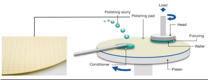
Source: Sensofar Metrology, Nomura research
Fig. 174: CMP processes vs IC technology nodes
Load
70
USD400-500mn
Source: Company data, Nomura estimates
FS: 15LM, BS: 4LM
Silicon Carrier
Backside power delivery and wafer-to-wafer technology to drive the growth of semi wafer, wafer bonding, grinding, and CMP process
An introduction to backside power delivery
A power delivery network is designed to provide power supply and reference voltage to the active devices on the die most efficiently. Traditionally, it is realized as a network of low-resistive metal wires fabricated through back-end-of-line (BEOL) processing on the frontside of the wafer. The power delivery network shares this space with the signal network, i.e., the interconnects that are designed to transport the signal. Due to the narrower pitches in the signal network, f energy lost resulting in a power delivery or IR drop when bringing power down.
A backside power delivery network is a solution to these issues. The idea is to decouple the power delivery network from the signal network by moving the entire power distribution network to the backside of the silicon wafer, which today serves only as a carrier. From there, it enables direct power delivery to the standard cells through wider, less resistive metal lines, without the electrons needing to travel through the complex BEOL stack. This approach reduces IR drop, improves power delivery performance, reduces routing congestion in the BEOL, and when properly designed, allows for further standard cell-height scaling.
As two silicon wafers are used in the back-side power delivery process - one is the silicon wafer acting as an interposer (first semi wafer) in between the signal network, and the other is acting as the permanent silicon carrier (second semi wafer) of the device - we expect the usage of silicon wafers will increase, along with wafer bonding. On the other hand, the wafer bonding, grinding and thinning process will increase as well to form the silicon interposer in between the signal and power network (Fig. 176 -5 ).
Fig. 176: The structure of TSMC’s super power rail
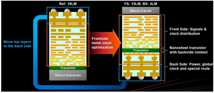
Source: TSMC
STEP 2
Permanent bonding
STEP 3
Backside passivation
Source: IMEC
We expect backside power delivery inflection point in 2027F, when TSMC start to ramp-up more A16 capacity
We expect 2027F will be the BPD inflection point, as TSMC’s A16 ramping-up at scale drives the dominant share of global BPD capacity and its associated semi wafer, bonding, thinning, and CMP demand. We expect the majority of high-performance computing (HPC) chips will adopt BPD technology, while other chips could continue to use the normal version node without the BPD function. As a result, for TSMC, we expect its A16 and A12 nodes will be BPD ready, while N2 and A14 nodes will not be equipped with BPD. By 2030F, global BPD capacity may contribute an additional low-single-digit percentage of total global 12’ semi wafer demand.
150
Talle
With BPD
Fig. 178: The key incremental processes required for BPD
Semi wafer
Wafer bonding
Grinding/thinning
0
CMP
Major beneficiaries
Shin-etsu,
SUMCO,
| 2 wafers | 2x Siltronic, GWC, | |
|---|---|---|
| 1 permanent bonding to 2nd Semi New process wafer | Disco, and | 2x, additional extrem grind required EVG, TEL, SUSS Microtec, etc. |
| 1 back grinding/thinning 2 back grinding/thinning | from 700um to few um only) | (reduce the thickness of 1st Semi wafer potentially Kinik, etc. |
| 55-70 total 2028F 2029F • Other foundries (assuming 30% of the market share) | 20-30% more CMP process per wafer Ebara, AMAT, Entegris, Kinik, etc. 2030F | 45-55 total 2026F 2027F |
| TSMC backside power delivery capacity (A16, A12) |
Source: Nomura estimates
Fig. 179: BPD capacity by TSMC and other foundries
Source: Nomura estimates
The wafer-bonded NAND inflection point in 2027F - memory and logic wafers are made separately and bonded together
The wafer-bonded NAND technology was introduced by YMTC for the first time in 2018, YMTC’s wafer bonded technology is called Xtacking, and can be also called CMOS directly bonded to array (CBA) technology, which makes the CMOS circuit (logic) wafers and memory cells array wafers can be manufactured separately and bonded together. Before the launch of CBA architecture, 3D NAND architectures in the market were divided into the traditional side-by-side structure and CnA (CMOS next to Array) architecture.
Since the two types of wafers are manufactured in parallel, there is also the added benefit of shortened production times compared to the conventional method. Performing hightemperature processing solely on the memory cell array wafer makes it possible to achieve the optimal temperature to ensure reliability without having to consider the impact on the CMOS circuit. By separating the wafer manufacturing processes, the performance of the CMOS circuit and the memory cell array can be maximized.
As a result, besides YMTC has already adopted CBA technology to produce its 3D NAND since 2018, Kioxia has produced some volume since 2H24 as well. However, we expect Kioxia may further increase its wafer-bonded NAND capacity more meaningfully by end2026F, with Samsung and Hynix following by 2027F. We believe this is likely to be positive for the following supply chain sectors:
1 wafer wallet
Multiplier vs. Conventional
The Gleam ooh space dia selll walel dellahlu Will be 40 70 more
2
1
0
Faster process time
Memory
Cell Array metal VIAs(Vertical Interconnect Accesses)
- Cleanroom space will be increased due to more wafer-to-wafer bonding processes are required to produce the same amount of NAND supply. 1. Memory wafer →
Cell array
- Semi wafer usage will be increased due to additional logic wafer will be used.
- Wafer-to-wafer bonding tool demand will be increased.
total global 12’ semi wafer demand. Source: Kioxia
Bit line
However, the cleanroom space and semi wafer demand growth would not be 100% but more likely to grow by around 40% more mainly due to the faster front-end process time to produce each CMOS and memory wafers (Fig. 183 ). By 2030F, global wafer-bonded NAND capacity may contribute an additional mid-to-high-single-digit percentage of
CNA structure
CBA Structure
• Memory wafer input
Logic wafer input
•Actual NAND wafer output
Fig. 180: 3D NAND: CNA vs CBA structure

Source: Kioxia
Fig. 182: YMTC’s Xtacking technology
Source: YMTC
Fig. 183: The wafer bonded NAND wafer input vs output
The cleanroom space and semi wafer demand will be 40% more
Source: Nomura estimates
Word line hook up interconnect
Cu bonding pad
Into one wafer
Bonding interface
CMOS
Fig. 181: The wafer-to-wafer bonding structure
Source: Kioxia
LULU LITT
90%
80%
70%
60%
50%
40%
30%
20%
10%
0%
2024F
(12” kwpm)
800
Fig. 184: Wafer-bonded NAND capacity % The wafer bonded NAND capacity will start to grow more meaningfully from 700
2026-27F 500
400
Source: Nomura estimates
Fig. 185: Incremental wafer-bonded NAND capacity vs incremental semi wafer demand
Source: Nomura estimates
16,000
14,000
12,000
10,000
8,000
6,000
4,000
2,000
0
USD400-500mn
Semi grinding wheel market is potentially as big as CMP pad conditioner market for Kinik
Currently, Kinik’s ABU business is mainly for industrial and automation applications rather than for semiconductors. Management is aiming to expand the ABU business into the semi market, such as working closely with major OSAT companies to address wafergrinding opportunities. According to our estimates, the semi wafer grinding wheel market is as big as the market for CMP pad conditioner - both over USD400mn in 2025.
According to leading global dicing and grinding equipment supplier Disco, around 35% of its total sales were from consumables in FY25, with grinding wheels accounting for around 30-40% of total consumables. As a result, we estimate Disco had around USD350mn in sales from grinding wheels. As Disco is the distant leader in the semi wafer grinding wheel market, accounting for around 80% of the market share, according to management, we think that a reasonable for the global semi grinding wheel market is around USD400-500mn, similar to the market for CMP pad conditioner. As Kinik remains a relatively insignificant player in this market, we think this could represent upside potential in terms of Kinik’s future business development.
•Others
Source: Company data, Nomura estimates
Fig. 188: Kinik: Sales breakdown by business unit
Source: Company data, Nomura estimates
Source: Company data, Nomura estimates
Net sales
COGS
Gross profit
SG&A
Op income
Net income
EPS (TWD)
Gross margin
Op margin
PBT margin
Net margin
(%)
Sales
Gross profit
Op income
Net income
YoY (%)
Sales
Gross profit
Op profit
Net profit
1,224
1,435
3Q25
2,091
1,414
4Q25!
2,172 i
1,429 !
548
680
677
7421
Earnings forecast
4Q26F!
2,520 i
1,580 -
940
330 !
48 i
562!
100
1027F
2,694
1.683
1,011
350
51
609
100
2Q27F
2,849
1,767
1,083
362
51
669
100
3Q27F
2,879
1,787
1,092
363
52
677
100
4027F!
2,930 H
1,818
1,112 |
363
53
696 1
100
796 1
1Q26
2,293
1,491
803
310
48
444
88
2026F
2,422
1,517
906
322
48
535
100
3Q26F
2,467
1,547
920
326
49
545
100
In 2026F, Kinik is likely to grow its sales toward the TWD10bn level, in our view, due to strong growth momentum of its DBU and SBU. We expect this momentum to continue in 2027-28F due to its leading foundry customer’s capacity expansion plan and the recovery of the semi wafer market. If its ABU can grow further by penetrating into the semi market, it may generate upside to sales and earnings in the long term. 26.3 21.0 27.0 21.6 27.0 21.6 143 636 1 27.2| 21.71
FY24
7,019
4,831
2,188
869
164
1,155
134
1,289
227
1,035
7.1
FY24
31.2
16.5
18.4
14.7
FY25
8,149
5.502
2,647
1,157
187
1,303
355
1,658
263
1,360
9.3
FY25
32.5
16.0
20.3
16.7
FY26F
9,702
6,135
3,568
1,288
194
2,086
387
2,473
439
1,987
13.3
FY26F
36.8
21.5
25.5
20.5
7,055
4,298
1,438
207
2,653
399
3,052
549
2,439
16.4
FY27F
37.9
23.4
26.9
21.5
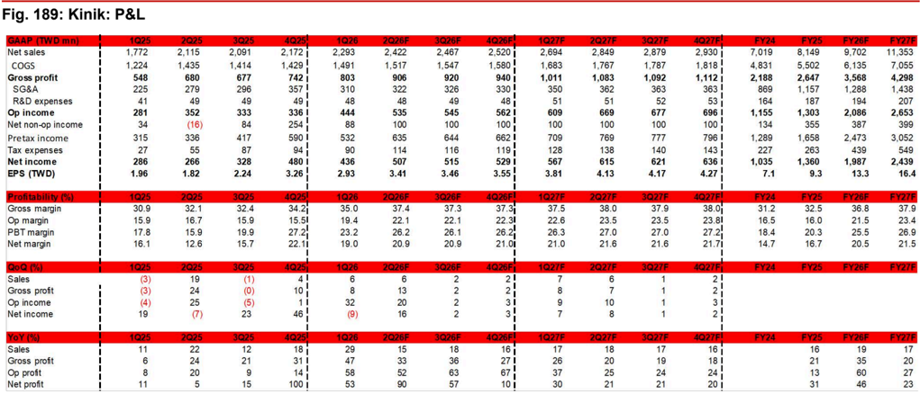
| Fig. 189: Kinik: P&L | Fig. 189: Kinik: P&L | Fig. 189: Kinik: P&L | Fig. 189: Kinik: P&L | Fig. 189: Kinik: P&L | Fig. 189: Kinik: P&L | Fig. 189: Kinik: P&L | Fig. 189: Kinik: P&L | Fig. 189: Kinik: P&L | Fig. 189: Kinik: P&L | Fig. 189: Kinik: P&L | Fig. 189: Kinik: P&L | Fig. 189: Kinik: P&L | Fig. 189: Kinik: P&L | Fig. 189: Kinik: P&L | Fig. 189: Kinik: P&L | Fig. 189: Kinik: P&L |
|---|
Source: Company data, Nomura estimates
Ticker
CMP slurry and CMP pad
0OL
1560 TT
ENTG US
009
8028 TT
MMM US
6140 JP
300054 CH
009
688019 CH
Mean
00t
Median
008
00Z
OOL
0
Rating
Buy
Kinik
Mkt Cap
USDmn
2,966
Valuation and risks
P/E (x)
P/S (x)
2026F
2027F
9.7
5.9
8.0
3.0
1.4
JUS/OML
2026F
2027F
8.3
0OL
47.2
6.3
36.9
5.3
009
1.4
41.0
16.8
23.0
28.8
38.4
31.7
15.4
21.2
P/B (x)
2026F
2027F
10.1
4.6
7.9
16.2
1.0
Current Price
(LC)
642.0
133.1
287.5
146.2
1,336.0
ROE (%)
2026F
2027F
22.8
12.9
23.3
89.8
4.8
1,507
394
8.5
4.1
6.3
11.9
1.0
Our TP of TWD840 is based on 40x 2028E EPS TWD21, in the upper half of its historical P/E of 10-45x, to address the stably growing business with the leading foundry customer as well as the rising total addressable market (TAM) across its different business units.
Downside risks are: 1) the products are disqualified by the leading foundry customer; 2) losing market share to competitors; 3) failure to broaden the product portfolio; 4) weakening semi market demand.
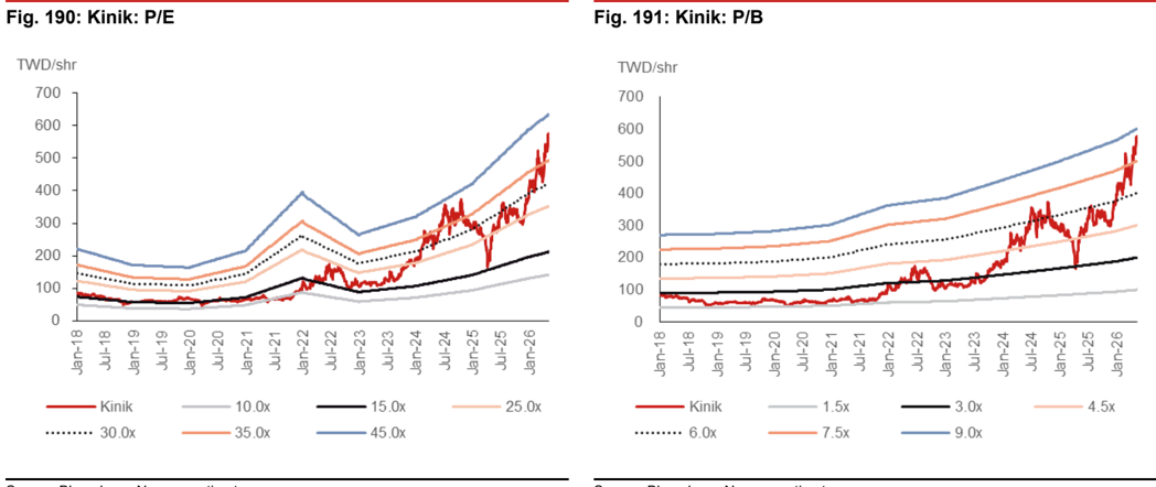
Source: Bloomberg, Nomura estimates
Fig. 192: A valuation comparison
Source: Nomura estimates and Bloomberg consensus as of 15 May 2026
Source: Bloomberg, Nomura estimates
24.2
15.0
25.1
79.1
4.8
15.8
30.0
27.7
24.2
2.9
EV/Sales (x)
2026F
2027F
9.7
6.9
8.8
3.4
1.2
15.4
15.3
8.7
8.8
8.3
6.1
7.0
3.3
1.1
12.1
12.3
7.2
7.0
2026F
0.8
0.3
1.5
2.2
2.5
n.a.
0.3
1.3
1.1
0.8
0.3
2.0
2.3
2.7
n.al
0.3
1.4
1.4
factory)
County
Appendix
Company Profile
Products
Use
Notes
Conventional grinding wheels (vitrified, resinoid, HQ, Manufacturing Designated historic site;
shellac, rubber, PVA bonded); diamond/CBN
grinding wheels; DLC coatings
(Abrasives &
Diamond B.U.)
Kinik is Taiwan’s leading grinding wheel and abrasive product manufacturer, with over 70 years of history. Originally founded in 1953 as China Grinding Wheel Corporation (rebranded KINIK in 1988) and headquartered in New Taipei City, the company has transformed from a traditional grinding wheel maker into a high-value-added supplier serving the semiconductor industry. Kinik’s business spans four key segments: 1) Conventional Abrasives (grinding wheels, cutting wheels), 2) Diamond Products (CMP diamond disk pad conditioners, diamond/CBN grinding wheels, DLC coatings, ultraprecision machining tools), 3) Reclaimed Wafers (8” and 12” reclaimed silicon wafers for semiconductor fabs), and 4) Semiconductor Materials. Kinik ranks in Top 2 of both CMP diamond pad conditioner and reclaimed wafer market share globally. The company serves over 8,000 customers with more than 100,000 product specifications with ~1,5001,600 employees. In 2025, revenue was approximately TWD8.1bn. cleanroom
Facilities and Offices
Fig. 193: Kinik: facilities and offices
Taichung / Changhua / Tainan / _
Kaohsiung original factory since
1953
Passed ISO 14064-1,
ISO 14001
ISO 9001, ISO 14001,
ISO 14064-1 certified
Reclaimed wafer cleanroom facility; ISO
50001 certified
Completed and in mass production; one of
world’s top three reclaimed wafer facilities
Corporate registration address
Registered Head
Office,
Administration
| service offices | Regional sales & Service centers across Taiwan |
|---|
Source: Company data
Approx.
Management team (Executive Committee)
Fig. 194: Kinik: management team
(combined)
Source: Company data
| Name | Occupation | Resume |
|---|---|---|
| Lin Po-Chuan | Chairman of the Board | Current Chairman of Kinik Company. Elected in the most recent Board re- election. Responsible for overall strategic direction, corporate governance and stakeholder relations. The Lin family has long-standing ties to the company, continuing the legacy of the founding Pai family. |
| Jung-Che Hsieh | Chief Executive Officer (CEO) & Director | CEO of Kinik Company. Led the company’s transformation from traditional grinding wheels into diamond-related semiconductor products and reclaimed wafers. Oversees all four business units: Abrasives, Diamond, Semiconductor Materials, and Optoelectronics. Has guided Kinik’s recognition as an TSMC outstanding supplier and winner of the National Quality Award. Frequently cited in media as the driving force behind Kinik’s ‘reinvention every 20 years.‘ |
| Pai Wen-Liang | Vice Chairman | Vice Chairman of the Board. Member of the founding Pai family. Previously served as director with significant shareholdings. |
| Pai Ching-Chung | Director | Board member. Member of the founding family. |
| Liao Po-Hsi | Independent Director | Independent board member. Provides oversight on audit and corporate governance. |
| Tsai Hsin-Yuan | Independent Director | Independent board member. |
| Hsiao Wen-Yi | Independent Director | Independent board member. |
Major shareholders
Fig. 195: Kinik: shareholders
Source: Bloomberg Finance L.P.
~4%
Relative performance chart
EQUITY: TECHNOLOGY
Price
(TWD)
800-
7001
6001
5001
4001
300-
120
-110
• 100
- 90
GlobalWafers 6488.TWO 6488 TT
EQUITY: TECHNOLOGY
Churra. I CEC Namura
Supply-demand dynamic continuously improving
Wafer demand and utilization rate are becoming more favorable; await further upward LTA price adjustment
Action: upgrade to Buy with and lift TP to TWD850; near-term profitability weakness not affecting new semi technology adoptions in 2027-28F
GlobalWafers has been negatively impacted by weak semi wafer market demand and low profitability since 2H24 (link). However, in addition to regular semi wafer demand growth and customers’ capex expansion cycles driven by strong AI demand, we see a few catalysts driven by the adoption of new semi technology, including: 1) wafer-bonded NAND; 2) backside power delivery (BPD); and 3) emerging photonics SOI demand. Although GWC’s profitability remains at a low level and semi wafer prices are unlikely to be revised up immediately as existing LTAs have not all been renewed yet (mainly for big memory/logic customers), we expect semi wafer companies’ bargaining power to recover gradually with some spot price hikes by 10% HoH driven by small memory customers in 2H26F. Hence, we upgrade GWC to Buy from Neutral and raise our TP to TWD850, based on 3.2x 2028F BVPS TWD265 (increased from previously 2.1x 2026F BVPS of TWD230 to factor in the potential upcycle in 2027-28F, where 3.2x was about the P/B multiple before GWC’s valuation plunged in 2H24). We expect GWC’s sales/net profit to post a 17%/36% CAGR in 2026-28F. The stock is trading at 2.4x 2027F BVPS.
Wafer-bonded NAND, BPD, and photonics SOI demand are emerging in 2027F
Based on our assumptions, we expect 2027F to be the inflection point for wafer-bonded NAND, BPD, and photonics SOI demand. Wafer-bonded NAND demand is likely to be driven when non-YMTC players start adopting a similar technology, which requires additional logic wafer to be bonded onto memory wafer. For BPD, TSMC’s A16 ramping at scale should also drive associated semi wafer, bonding, thinning, and CMP demand. Last, photonics SOI wafer is becoming an increasingly important material to build SiPh-based PIC, due to its scalability in most of major foundries with lower cost per die, with GWC one of major global SOI wafer suppliers. We expect these three emerging demand drivers will lead to additional 2-3pp demand growth annually over 2026-30F.
Semi wafer supply/demand: supply tightness likely to be seen over 2027-28F
We expect 12’ semi wafer demand to increase by around 10% per year from 2026F to 2030F. If we assume most leading semi wafer companies reach their capacity limitation by around 2028F, then supply-demand should become more favorable in 2027-28F. Some further price hikes in the spot market could also be likely in 2H26F.
| Year-end 31 Dec Currency (TWD) | FY25 Actual | Old | FY26F New | Old | FY27F New | Old | FY28F New |
|---|---|---|---|---|---|---|---|
| Revenue (mn) | 60,598 | 78,314 | 61,159 | 0 | 71,372 | 0 | 83,460 |
| Reported net profit (mn) | 7,311 | 17,579 | 8,248 | 0 | 10,825 | 0 | 15,322 |
| Normalised net profit (mn) | 7,311 | 17,579 | 8,248 | 0 | 10,825 | 0 | 15,322 |
| FD normalised EPS | 15.36 | 40.20 | 17.25 | 22.64 | 32.05 | ||
| FD norm. EPS growth (%) | -29.8 | 35.2 | 12.3 | 31.3 | 41.5 | ||
| FD normalised P/E (x) | 46.2 | - | 41.2 | - | 31.4 | - | 22.2 |
| EV/EBITDA (x) | 24.9 | - | 25.5 | - | 19.5 | - | 14.6 |
| Price/book (x) | 3.3 | - | 3.2 | - | 2.9 | - | 2.7 |
| Dividend yield (%) | 1.0 | - | 1.1 | - | 1.6 | - | 2.0 |
| ROE (%) | 7.9 | 17.8 | 8.6 | 10.6 | 13.9 | ||
| Net debt/equity (%) | 7.1 | net cash | 3.8 | 0.3 | net cash |
Source: Company data, Nomura estimates
Apr
May
Global Markets Research 21 May 2026
| Rating Up from Neutral | Buy |
|---|---|
| Target price Increased from TWD 480.00 | TWD 850.00 |
| Closing price 15 May 2026 | TWD 710.00 |
| Implied upside | +19.7% |
| Market Cap (USD mn) | 10,760.1 |
| ADT (USD mn) | 118.6 |
Relative performance chart
Source: LSEG, Nomura
Research Analysts
Semiconductor
Donnie Teng - NIHK donnie.teng@nomura.com +852 2252 1439
Aaron Jeng, CFA - NITB
aaron.jeng@nomura.com +886(2) 21769962
Key data on GlobalWafers
Performance
| (%) | 1M | 3M | 12M | ||
|---|---|---|---|---|---|
| Absolute (TWD) | 37.6 | 59.4 | 114.5 | M cap (USDmn) | 10,760.1 |
| Absolute (USD) | 38 | 58.7 | 104.9 | Free float (%) | 27.5 |
| Rel to Taiwan TAIEX Index | 25.5 | 36.9 | 25 | 3-mth ADT (USDmn) | 118.6 |
Income statement (TWDmn)
| Year-end 31 Dec | FY24 | FY25 | FY26F | FY27F | FY28F |
|---|---|---|---|---|---|
| Revenue | 62,626 | 60,598 | 61,159 | 71,372 | 83,460 |
| Cost of goods sold | -42,823 | -45,974 | -47,519 | -53,753 | -59,867 |
| Gross profit | 19,804 | 14,624 | 13,640 | 17,619 | 23,593 |
| SG&A | -3,365 | -3,770 | -3,533 | -3,726 | -4,173 |
| Employee share expense | -2,320 | -2,218 | -2,178 | -2,355 | -2,668 |
| Operating profit | 14,119 | 8,636 | 7,929 | 11,537 | 16,752 |
| EBITDA | 18,987 | 13,797 | 13,451 | 17,396 | 22,827 |
| Depreciation | -4,829 | -5,120 | -5,478 | -5,812 | -6,026 |
| Amortisation | -39 | -41 | -44 | -47 | -48 |
| EBIT | 14,119 | 8,636 | 7,929 | 11,537 | 16,752 |
| Net interest expense | 2,489 | 1,124 | 2,130 | 2,341 | 2,891 |
| Associates & JCEs | 186 | 85 | 0 | 0 | 0 |
| Other income | -4,364 | -329 | 431 | 0 | 0 |
| Earnings before tax | 12,429 | 9,516 | 10,490 | 13,879 | 19,644 |
| Income tax | -2,590 | -2,205 | -2,242 | -3,053 | -4,322 |
| Net profit after tax | 9,839 | 7,311 | 8,248 | 10,825 | 15,322 |
| Minority interests | 7 | 0 | 0 | 0 | 0 |
| Other items | 0 | 0 | 0 | 0 | 0 |
| Preferred dividends | 0 | 0 | 0 | 0 | 0 |
| Normalised NPAT | 9,847 | 7,311 | 8,248 | 10,825 | 15,322 |
| Extraordinary items | 0 | 0 | 0 | 0 | 0 |
| Reported NPAT | 9,847 | 7,311 | 8,248 | 10,825 | 15,322 |
| Dividends | -5,259 | -3,290 | -3,711 | -4,871 | -6,333 |
| Transfer to reserves | 4,588 | 4,021 | 4,536 | 5,954 | 8,989 |
| Valuations and ratios | |||||
| Reported P/E (x) | 32.1 | 46.2 | 41.2 | 31.4 | 22.2 |
| Normalised P/E (x) | 32.1 | 46.2 | 41.2 | 31.4 | 22.2 |
| FD normalised P/E (x) | 32.4 | 46.2 | 41.2 | 31.4 | 22.2 |
| Dividend yield (%) | 1.5 | 1.0 | 1.1 | 1.6 | 2.0 |
| Price/cashflow (x) | 12.3 | - | 21.7 | 23.2 | 17.6 |
| Price/book (x) | 3.4 | 3.3 | 3.2 | 2.9 | 2.7 |
| EV/EBITDA (x) | 17.6 | 24.9 | 25.5 | 19.5 | 14.6 |
| EV/EBIT (x) | 23.6 | 39.7 | 43.3 | 29.4 | 19.9 |
| Gross margin (%) | 31.6 | 24.1 | 22.3 | 24.7 | 28.3 |
| EBITDA margin (%) | 30.3 | 22.8 | 22.0 | 24.4 | 27.4 |
| EBIT margin (%) | 22.5 | 14.3 | 13.0 | 16.2 | 20.1 |
| Net margin (%) | 15.7 | 12.1 | 13.5 | 15.2 | 18.4 |
| Effective tax rate (%) | 20.8 | 23.2 | 21.4 | 22.0 | 22.0 |
| Dividend payout (%) | 53.4 | 45.0 | 45.0 | 45.0 | 41.3 |
| ROE (%) | 12.5 | 7.9 | 8.6 | 10.6 | 13.9 |
| ROA (pretax %) | 8.2 | 4.5 | 4.0 | 5.7 | 8.0 |
| Growth (%) | |||||
| Revenue | -11.4 | -3.2 | 0.9 | 16.7 | 16.9 |
| EBITDA | -24.0 | -27.3 | -2.5 | 29.3 | 31.2 |
| Normalised EPS | -51.8 | -30.6 | 12.3 | 31.3 | 41.5 |
| Normalised FDEPS | -51.8 | -29.8 | 12.3 | 31.3 | 41.5 |
Source: Company data, Nomura estimates
Cashflow statement (TWDmn)
| Year-end 31 Dec | FY24 | FY25 | FY26F | FY27F | FY28F |
|---|---|---|---|---|---|
| EBITDA | 18,987 | 13,797 | 13,451 | 17,396 | 22,827 |
| Change in working capital Other operating cashflow | 11,289 -4,298 | -28,021 | 1,872 | -2,057 -712 | -2,115 -1,430 |
| Cashflow from operations | 25,978 | -1,297 -15,521 | 320 15,643 | 14,627 | 19,281 |
| Capital expenditure | -48,319 | -25,073 | -21,035 | -17,518 | |
| -22,342 | -33,130 -48,650 | -9,430 | -6,408 | 1,764 | |
| Free cashflow | |||||
| Reduction in investments | -6,052 | 498 | 0 | 0 | 0 |
| Net acquisitions | 0 | 0 | 0 | 0 | 0 |
| Dec in other LT assets | 4,302 0 | 39,845 | 15,672 | 13,508 | 8,809 |
| Inc in other LT liabilities | 0 | 0 | 0 | ||
| Adjustments | 0 | 0 | 0 | 0 | 0 |
| CF after investing acts | -24,092 | -8,307 | 6,242 | 7,101 | 10,573 |
| Cash dividends | -8,748 | -5,259 | -3,290 | -3,711 | -4,871 |
| Equity issue | 0 | 0 | 0 | 0 | 0 |
| 9,776 | -11,511 | 0 | 0 | 0 | |
| Debt issue | 0 | 0 | |||
| Convertible debt issue Others | 35,829 | 5,632 | 0 | 0 | 0 |
| CF from financial acts | 36,857 | 0 -3,291 | 0 -3,712 | 0 -4,871 | |
| Net cashflow | 12,765 | -11,138 -19,445 | 2,952 | 3,389 | 5,702 |
| Beginning cash | 26,165 | 38,929 | 19,484 | 22,436 | 25,824 |
| Ending cash | 38,929 | 19,484 | 22,436 | 25,824 | 31,526 |
| Ending net debt | |||||
| Balance sheet | |||||
| -1,282 | |||||
| (TWDmn) As at 31 Dec | FY24 | 6,652 FY25 | 3,700 FY26F | 312 FY27F | -5,390 FY28F |
| Cash & equivalents Marketable securities | 38,929 29 | 19,484 1 | 22,436 0 9,469 | 25,824 0 11,042 | 31,526 0 12,919 |
| Accounts receivable | 10,265 | 10,113 | 9,666 | 12,019 | |
| Inventories Other current | 11,238 20,030 | 10,399 46,632 | 46,632 | 10,898 46,632 | 46,632 |
| assets Total current assets | 80,492 | 86,629 | 94,397 | 103,096 | |
| LT investments | 7,445 | 6,947 | 88,203 6,947 | 6,947 | 6,947 |
| Fixed assets | 119,074 | 107,241 | 111,120 | 112,788 | 115,421 |
| Goodwill | 0 | 0 | 0 | 0 0 | 0 |
| Other intangible assets | 0 | 0 | 0 | 0 | |
| Other LT assets | 17,570 | 17,525 | 17,525 | 17,525 | 17,525 |
| Total assets | 224,581 | 218,343 | 223,794 | 231,656 | 242,990 |
| Short-term debt | 27,117 | 18,571 | 18,571 | 18,571 | 18,571 |
| Accounts payable | 4,161 | 4,655 | 5,404 | 6,286 | |
| Other current liabilities | 5,371 32,577 | 31,377 | 31,377 | 31,377 | 31,377 |
| Total current liabilities | 54,109 | 54,604 | 55,352 | 56,234 | |
| Long-term debt | 65,065 10,531 | 7,565 | |||
| Convertible debt | 0 | 0 | 7,565 0 | 7,565 0 | 7,565 0 |
| Other LT liabilities | 57,958 | 63,374 | 63,374 | 63,374 126,291 | 63,374 127,173 |
| Total liabilities | 133,553 | 125,048 | 125,543 -3 | -3 | -3 |
| Minority interest | -3 | -3 | |||
| Preferred stock | 0 | 0 | 0 | 0 | 0 |
| Common stock | 4,781 | 4,781 | 4,781 41,987 | 4,781 47,941 | 4,781 56,930 |
| Retained earnings | 31,640 | 3,290 | 3,711 | 4,871 | 6,333 |
| Proposed dividends | 5,259 | 37,451 | |||
| Other equity and Total shareholders’ | 49,350 91,030 | 47,776 93,298 | 47,776 98,255 | 47,776 105,369 | 47,776 115,820 |
| reserves equity | |||||
| Total equity & liabilities | 224,580 | 231,656 | 242,990 | ||
| Liquidity (x) | |||||
| 218,342 | 223,794 | ||||
| Current ratio | 1.24 - net cash net cash | 1.60 - 0.48 7.1 | 1.62 - 0.28 | 1.71 - 0.02 0.3 | 1.83 - net cash net cash |
| Interest cover Leverage Net debt/EBITDA (x) | 3.8 | ||||
| Net debt/equity (%) Per share Reported EPS (TWD) | 22.14 22.14 21.90 | 15.36 15.36 | 17.25 17.25 | 22.64 22.64 | 32.05 32.05 |
| Norm EPS (TWD) FD norm EPS (TWD) BVPS (TWD) | 208.19 | 15.36 213.37 6.88 | 17.25 224.71 7.76 | 240.98 | 264.88 |
| DPS (TWD) | 11.00 | 22.64 | 32.05 | ||
| 14.48 | |||||
| 11.14 | |||||
| Activity (days) | |||||
| 61.4 | 58.4 77.1 | 52.4 69.8 | 52.5 70.1 | ||
| Days receivable Days inventory | 59.4 87.8 | 85.9 | 33.9 | 35.7 | |
| Days payable | 44.3 | 37.8 109.4 | 34.2 | ||
| Cash cycle | |||||
| 102.9 | |||||
| 88.1 | |||||
| 101.6 | |||||
| 86.9 |
Source: Company data, Nomura estimates
Company profile
GlobalWafers is the world’s third-largest and largest non-Japanese wafer manufacturer that specializing in 3’ to 12’ silicon wafer manufacturing, possessing a complete production line from ingot growth, slicing, etching, diffusion, polishing and epitaxy.
Valuation Methodology
Our TP of TWD850 is based on 3.2x 2028F BVPS TWD265. The 3.2x P/B is based on the lower-half of 2-6x P/B range during the full Semi wafer cycle in 2017-2020. The benchmark index is TAIEX.
Risks that may impede the achievement of the target price
Downside risks include: · Faster-than-expected entry of China into the 12’ semi wafer market. · Slower-than-expected of market consolidation. · Worse-than-expected end-demand for the semi industry. · Less favorable demand/supply dynamics in the semi wafer industry. · Less favorable FX volatility and rising material/utility costs.
ESG
In response to global climate change and latest development trends in corporate social responsibilities (CSR), GlobalWafers has taken the initiative to compile a CSR report. Based on long-term in-depth interactions with local communities and engagement with stakeholders, GlobalWafers discloses in the report relevant information on material issues regarding the four aspects of corporate governance, economy, environment, and society, as well as execution & improvement results, in addition to presenting the the future vision and goals in terms of sustainable development.
30%
14
25%
12
20%
10
8
15%
6
10%
4
5%
2
0
0%
12’ semi wafer supply demand could turn more favorable sometime in 2027-28F
We expect there are five major drivers of 12’ semi wafer demand over 2026-30F, including: 85%
- The regular 12’ semi wafer market growing on an average at around 5% per year. ·
- Semi companies’ capacity expansion across leading foundries and memory makers, which could add another 2-3pp growth per year. This incremental growth was seen during the COVID period in 2020-22, when most of the semi companies added capacity to meet rising WFH demand. · growth annual growth
- Wafer-bonded NAND could add another 1-2pp growth per year, due to additional logic wafer that will be used. ·
- The BPD process and photonics SOI demand could add another 0-1pp growth per year, purely driven by new technology adoption. ·
As a result, it is possible that the 12’ semi wafer demand could grow by around 10% each year from 2026 to 2030F. Assuming most of the leading semi wafer companies reach their capacity limitation by around 2028F, we expect supply-demand could turn more favorable sometime in 2027-28F.
Fig. 196: 12’ semi wafer market growth catalysts
Source: Nomura estimates
Fig. 197: 12’ semi wafer supply demand trend
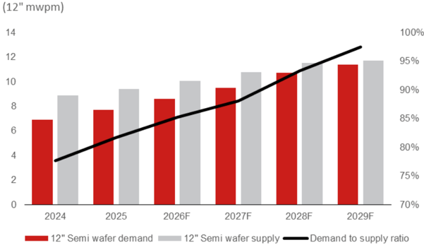
Net Sales
EPS
4,112
2Q25
16,008
4,123
3Q25
14,493
2,662
4Q25
14,502
3,726
1Q26F
13,985
2,914
Earnings forecast revisions
2Q26F 3Q26F 4Q26F
15,125
1,987
16,381
15,669
3,394
2,575
2,008
3,552
2,095
2,687
2,096
3,780
2,372
2,882
2,248
2025
60,598
14,624
8,636
9,516
7,312
We adjust our earnings model to factor in actual financial numbers for 2025. We expect a moderate revenue recovery in 2026F, but with more acceleration from 2H26F onwards, along with a more favorable supply-demand environment in 2027-28F. Profitability is still under pressure due to rising depreciation costs from new capacity expansion, but once market demand continues to grow, we believe price hike opportunity is also likely to increase. 15.36
Fig. 198: GWC: P&L
-27.8%
Pretax income
Net income
Growth (YoY)
Net Sales
Gross profit
Op income
Pretax income
Net income
3.6%
4.7%
5.4%
4.5%
6.4%
13.2%
2.7%
0.3%
-5.8%
-9.5%
-35.4%
49.6%
0.1%
40.0%
93.5%
-3.6%
-21.8%
-38.0%
8.2%
16.5%
34.7%
| 168.0% | 7.3% | 4.4% | 32.9% | -19.3% | 9.7% | 4.4% | 7.2% | ||||
|---|---|---|---|---|---|---|---|---|---|---|---|
| 204.2% | 15.5% | 17.1% | 12.0% | -14.0% | 5.9% | 4.4% | 7.2% | ||||
| 3.4% | 4.5% | -8.7% | -11.3% | -10.3% | -5.5% | 8.1% | 13.0% | -3.2% | 0.9% | 16.7% | 16.9% |
| -20.4% | -16.7% | -44.2% | -24.2% | -29.1% | -17.7% | 33.4% | 1.5% | -26.2% | -6.7% | 29.2% | 33.9% |
| -34.7% | -27.6% | -61.6% | -33.6% | -43.0% | -18.5% | 70.3% | 0.3% | -38.8% | -8.2% | 45.5% | 45.2% |
| -35.2% | -38.3% | 265.2% | 10.0% | 12.5% | 22.8% | -0.9% | -23.4% | 10.2% | 32.3% | 41.5% | |
| -58.8% | 41.6% | -33.3% | 360.5% | 30.2% | 19.4% | 6.4% | 1.9% | -25.7% | 12.8% | 31.3% | 41.5% |
Source: Nomura estimates, company data
Valuation methodology and risks
Our new TP of TWD850 is based on 3.2x 2026F BVPS of TWD265. The 3.2x target multiple is at the lower-half of the historical P/B range of 2-6x during the full semi wafer cycle in 2017-20.
Downside risks include:
- Faster-than-expected entry of China into the 12’ semi wafer market.
- Slower-than-expected of market consolidation.
- Worse-than-expected end-demand for the semi industry.
- Less favorable demand/supply dynamics in the semi wafer industry.
- Less favorable FX volatility and rising material/utility costs.
2026F
61,159
13,640
7,929
10,490
8,248
22.3%
13.0%
17.2%
13.5%
17.25
2027F
71,372
17,619
11,537
13,879
10,825
24.7%
16.2%
19.4%
15.2%
22.64
23,593
16,752
19,644
15,322
28.3%
- 1%
23.5%
18.4%
32.05
Ticker
35
Wafer and Substrate
6488 TT
30
Globalwafers
SOI FP
688126 CH|
25
3532 TT
AXT US
20
002428 CH
SOITEC
Fig. 199: GWC: P/E
AXT Inc
Yunnan Lincang Xinyuan Germanium
Mean
15
Median
10
10/28/2015
10/28/2014
P/S (x)
2026F
2027F
5.3
8.7
15.9
6.3
56.2
56.7
24.9
4.6
7.9
12.4
n.a.
35.5
52.7
22.6
12.4
Rating
Buy
Buy
Neutral
Not Rated
Not Rated
Not Rated
Mkt Cap
USDmn
10,323
6,152
11,917
2,581
8,098
8,932
Current Price
(LC)
710.0
148.1
24.1
221.5
123.8
90.3
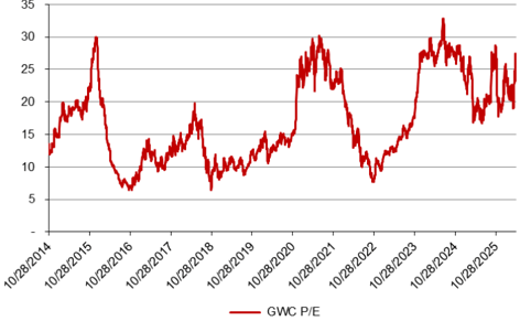
Source: Bloomberg Finance L.P., Nomura estimates
Fig. 201: Peer valuation comparison
Source: Nomura estimates and Bloomberg consensus as of 15 May 2026
9
7
6
5
4
3
180.9
2
1
10/28/2014
10/28/2015
2026F
P/E (x)
41.2
n.a.
P/B (x)
2026F
2027F
3.2
2.9
ROE (%)
2026F
2027F
8.6
10.6
3.5
2027F
31.4
3.3
(4.4)
3.7
Fig. 200: GWC: P/B vs ROE
164.6
n.a.
n.a.
3.3
n.a.
114.8
35
30
25
20
1.6
0.0
0.0
n.a.
n.a n.a
38.6
12.5
36.6
11.9
5.2
2.7
5.8
7.0
5.7
2026F
EV/Sales (x)
2027F
5.5
8.7
17.2
7.8
57.0
56.7
25.5
4.7
7.9
13.4
n.a.
35.7
53.1
22.9
2026F
1.1
0.0
0.0
0.9
n.a.
n.a
0.5
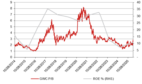
Source: Bloomberg Finance L.P., Nomura estimates
0.5
15
94.5
Relative performance chart
EQUITY: BASIC MATERIALS
Price
(CNY)
70-
60-
50-
40-
30 -
- 200
-175
- 150
-125
300054.SZ 300054 CH
Hubei Dinglong
EQUITY: BASIC MATERIALS
Courca. I CEC Namura
CMP scale-up and photoresist breakthrough
Pad share gains broaden; photoresist commercialization enters volume phase
CMP franchise scaling: pad capacity, slurry wins broaden runway
Dinglong delivered a robust 1Q26 with revenue of CNY1,020mn (+23.8% y-y) and net profit of CNY251mn (+78.0% y-y), driven by a step-change in the CMP (chemical mechanical polishing) consumables franchise. CMP pad sales reached CNY376mn (+71.2% y-y, +27.0% q-q), with monthly shipments breaking 40k pieces and capacity lifted to 50k/month by end-1Q26, in our view evidencing share gains at domestic foundries amid an industry-wide capacity build-out. CMP slurry and cleaner revenue jumped 54.2% y-y to CNY85mn, and we believe the May 7 wins in large-silicon-wafer fine slurry (12-inch single-crystal), ceria slurry at a leading domestic memory player, and TSV (through-silicon via) slurry at a leading advanced-packaging house unlock a domestic TAM (total addressable market) of over CNY1bn currently dominated by imports.
Photoresist inflecting: three SKUs in stable mass supply
High-end wafer photoresist remains the most strategically important option, in our view. Dinglong has built more than 30 immersion ArF (193nm) and KrF (248nm) SKUs, with over 20 sampled to clients and more than 12 in gallon-sample testing; three ArF/KrF products are already in stable mass supply, and management expects several more order conversions within 2026E. The Qianjiang Phase-1 30 tons/annum line is running smoothly and the Phase-2 300 tons/annum line is complete, providing capacity headroom we estimate at >5x current run-rate. We believe penetration will accelerate as domestic localization rates remain low at ~15% for KrF and only 2-3% for ArF, and as overseas’ potential tightening of exports in 2026-27F could create further price uplift window.
Reiterate Buy; TP raised to CNY104 on 96x 2026F P/E
We maintain our Buy rating and lift our TP to CNY104 (from CNY42), which reflects: 1) CMP pad shipments at record highs; 2) broadening of slurry pipelines; and 3) likely accelerated domestic photoresist substitution. We revise 2026F/27F earnings to CNY1,022mn/CNY1,312mn from CNY1,015mn/CNY1,322mn to reflect the improving margins, offset by growing depreciation. Our new TP is based on 96x 2026F P/E (vs previously 35x 2026F P/E), at +2.5x SD of its 5-year historical average, backed by a 33% earnings CAGR over 2025-28F. The stock is trading at 64x 2026F P/E. Risks: slower ramp-up of ArF/KrF order conversion; goodwill or integration risk from the lithium materials company acquisition.
| Year-end 31 Dec | FY25 Actual | FY26F New | FY27F New | Old | FY28F New | ||
|---|---|---|---|---|---|---|---|
| Currency (CNY) Revenue (mn) | 3,660 | Old 4,966 | 4,514 | Old 6,057 | 5,728 | 0 | 6,983 |
| Reported net profit (mn) | 720 | 1,015 | 1,022 | 1,322 | 1,312 | 0 | 1,675 |
| Normalised net profit (mn) | 720 | 1,015 | 1,022 | 1,322 | 1,312 | 0 | 1,675 |
| FD normalised EPS | 76.48c | 1.07 | 1.08 | 1.40 | 1.39 | 1.77 | |
| FD norm. EPS growth (%) | 38.3 | 40.2 | 41.8 | 30.3 | 27.8 | 27.6 | |
| FD normalised P/E (x) | 91.1 | - | 64.3 | - | 50.3 | - | 39.4 |
| EV/EBITDA (x) | 56.8 | - | 44.3 | - | 34.3 | - | 27.2 |
| Price/book (x) | 11.9 | - | 9.2 | - | 7.0 | - | 5.4 |
| Dividend yield (%) | - | - | - | - | - | - | - |
| ROE (%) | 13.9 | 18.9 | 16.1 | 21.5 | 15.8 | 15.4 | |
| Net debt/equity (%) | 9.0 | net cash | net cash | net cash | net cash | net cash |
Source: Company data, Nomura estimates
Global Markets Research 21 May 2026
| Rating Remains | Buy |
|---|---|
| Target price Increased from CNY 42.00 | CNY 104.00 |
| Closing price 15 May 2026 | CNY 69.68 |
| Implied upside | +49.3% |
| Market Cap (USD mn) | 9,708.5 |
| ADT (USD mn) | 277.8 |
Relative performance chart
Research Analysts
Semiconductor
Frank Fan - NIHK frank.fan@nomura.com +852 2252 2195
Donnie Teng - NIHK
donnie.teng@nomura.com +852 2252 1439
Key data on Hubei Dinglong
Performance
| (%) | 1M | 3M | 12M | ||
|---|---|---|---|---|---|
| Absolute (CNY) | 34.4 | 53 | 147.5 | M cap (USDmn) | 9,708.5 |
| Absolute (USD) | 34.7 | 55.3 | 162.2 | Free float (%) | 68.8 |
| Rel to CSI 300 | 30.7 | 48.7 | 123.2 | 3-mth ADT (USDmn) | 277.8 |
Income statement (CNYmn)
| Year-end 31 Dec | FY24 | FY25 | FY26F | FY27F | FY28F |
|---|---|---|---|---|---|
| Revenue | 3,338 | 3,660 | 4,514 | 5,728 | 6,983 |
| Cost of goods sold | -1,773 | -1,799 | -2,134 | -2,666 | -3,197 |
| Gross profit | 1,565 | 1,861 | 2,380 | 3,062 | 3,786 |
| SG&A | -890 | -971 | -1,178 | -1,483 | -1,795 |
| Employee share expense | |||||
| Operating profit | 674 | 890 | 1,202 | 1,578 | 1,992 |
| EBITDA | 918 | 1,172 | 1,490 | 1,896 | 2,334 |
| Depreciation | -192 | -226 | -236 | -274 | -306 |
| Amortisation | -51 | -55 | -52 | -43 | -36 |
| EBIT | 674 | 890 | 1,202 | 1,578 | 1,992 |
| Net interest expense | -12 | -50 | -95 | -121 | -147 |
| Associates & JCEs | |||||
| Other income | 53 | 65 | 100 | 125 | 150 |
| Earnings before tax | 715 | 905 | 1,207 | 1,582 | 1,994 |
| Income tax | -76 | -110 | -145 | -190 | -239 |
| Net profit after tax | 639 | 796 | 1,062 | 1,392 | 1,755 |
| Minority interests | -118 | -75 | -40 | -80 | -80 |
| Other items | |||||
| Preferred dividends | |||||
| Normalised NPAT | 521 | 720 | 1,022 | 1,312 | 1,675 |
| Extraordinary items | |||||
| Reported NPAT | 521 | 720 | 1,022 | 1,312 | 1,675 |
| Dividends Transfer to reserves | 521 | 720 | 1,022 | 1,312 | 1,675 |
| Valuations and ratios | |||||
| Reported P/E (x) | 126.0 | 91.1 | 64.3 | 50.3 | 39.4 |
| Normalised P/E (x) | 126.0 | 91.1 | 64.3 | 50.3 | 39.4 |
| FD normalised P/E (x) | 126.0 | 91.1 | 64.3 | 50.3 | 39.4 |
| Dividend yield (%) | - | - | - | - | - |
| Price/cashflow (x) | 79.2 | 56.7 | 42.8 | 33.5 | 26.3 |
| Price/book (x) | 13.5 | 11.9 | 9.2 | 7.0 | 5.4 |
| EV/EBITDA (x) | 72.0 | 56.8 | 44.3 | 34.3 | 27.2 |
| EV/EBIT (x) | 98.0 | 74.8 | 54.9 | 41.2 | 31.9 |
| Gross margin (%) | 46.9 | 50.9 | 52.7 | 53.5 | 54.2 |
| EBITDA margin (%) | 27.5 | 32.0 | 33.0 | 33.1 | 33.4 |
| EBIT margin (%) | 20.2 | 24.3 | 26.6 | 27.6 | 28.5 |
| Net margin (%) | 15.6 | 19.7 | 22.6 | 22.9 | 24.0 |
| Effective tax rate | 10.7 | 12.1 | 12.0 | 12.0 | 12.0 |
| (%) Dividend payout (%) | 0.0 | 0.0 | 0.0 | 0.0 | 0.0 |
| ROE (%) | 10.7 | 13.9 | 16.1 | 15.8 | 15.4 |
| ROA (pretax %) | 11.3 | 12.8 | 14.8 | 16.6 | 18.0 |
| Growth (%) | |||||
| Revenue | 25.1 | 9.7 | 23.3 | 26.9 | 21.9 |
| EBITDA | 98.0 | 27.7 | 27.2 | 27.2 | 23.1 |
| Normalised EPS | 133.3 | 38.3 | 41.8 | 27.8 | 27.6 |
| Normalised FDEPS | 133.3 | 38.3 | 41.8 | 27.8 | 27.6 |
Source: Company data, Nomura estimates
Cashflow statement (CNYmn)
| Year-end 31 Dec | FY24 | FY25 | FY26F | FY27F | FY28F |
|---|---|---|---|---|---|
| EBITDA | 918 | 1,172 | 1,490 | 1,896 | 2,334 |
| Change in working capital | -203 | -431 | -326 | -505 | -515 |
| Other operating cashflow | 114 | 416 | 369 | 578 | 694 |
| Cashflow from operations | 828 | 1,157 | 1,533 | 1,968 | 2,512 |
| Capital expenditure | -769 | -775 | -780 | -740 | -700 |
| Free cashflow | 60 | 381 | 753 | 1,228 | 1,812 |
| Reduction in investments | 0 | 0 | 0 | 0 | |
| Net acquisitions | |||||
| Dec in other LT assets | -332 | -270 | -417 | -431 | |
| Inc in other LT liabilities | 95 -302 | 0 -647 | 0 270 | 0 417 | 431 |
| Adjustments acts | 1,228 | 1,812 | |||
| CF after investing | -243 | -503 | 753 | -335 | |
| Cash dividends | -80 | -143 | -204 | -262 | |
| Equity issue | 9 | 176 | 0 | 0 | 0 |
| Debt issue | 414 | 1,001 | 0 | 0 | 0 |
| Convertible debt issue | -182 | -13 1,021 | 0 -204 | 0 | 0 |
| Others CF from financial acts | 161 | -262 | -335 | ||
| Net cashflow | -82 | 517 | 549 | 966 | 1,477 |
| Beginning cash | 1,120 | 2,104 | 3,070 | ||
| Ending cash | 1,038 | 1,038 | 1,555 | 3,070 | |
| Ending net debt | 1,555 | 2,104 | 4,547 | ||
| -2,495 | |||||
| Balance sheet | 303 | 496 | -52 | -1,018 | |
| (CNYmn) As at 31 Dec | FY24 | FY25 | FY26F | ||
| Cash & equivalents Marketable securities | 1,038 | 1,555 | 2,104 | FY27F 3,070 | FY28F 4,547 |
| Accounts receivable Inventories | 1,070 563 274 | 1,018 654 589 | 1,232 781 713 | 1,564 980 904 | 1,906 1,169 1,103 8,725 |
| Other current assets Total current assets | 2,944 | 4,829 | 6,517 | ||
| 3,815 | |||||
| LT investments | 2,639 | 3,133 | 3,677 537 | 4,143 537 | 4,537 |
| Fixed assets Goodwill | 537 | 537 | 537 | ||
| 299 | 247 | 204 | 168 | ||
| Other intangible assets Other LT assets | 327 948 | 1,281 | 1,550 | 1,967 | 2,399 |
| Total assets | 7,395 | 9,066 | 10,841 | 13,368 | 16,365 |
| Short-term debt | 402 | 226 | 226 | 226 | 226 |
| Accounts payable | 356 | 359 | 429 | 538 | 642 |
| Other current | 619 | 907 | |||
| liabilities liabilities | 699 | 689 1,344 | 796 1,561 | 1,776 | |
| Total current Long-term debt | 1,457 | 1,205 1,825 | 1,825 | ||
| 637 | 1,825 | 1,825 | |||
| Convertible debt Other LT liabilities | 426 | 521 | 521 | 521 | 521 |
| Total liabilities | 2,520 | 3,551 | 3,690 | ||
| 3,907 | |||||
| 4,122 | |||||
| Minority interest Preferred stock Common stock Retained earnings Proposed dividends | 938 2,094 1,843 | 947 2,719 | 947 3,537 2,667 | 947 4,587 3,928 9,462 | 947 5,926 5,370 12,244 |
| Other equity and reserves Total shareholders’ equity Total equity & liabilities | 4,875 7,395 | 1,849 5,515 9,066 | 7,151 | ||
| 10,841 | 16,365 | ||||
| Liquidity (x) | 13,368 | ||||
| Current ratio Interest cover | 2.02 57.2 | 3.17 17.9 | 3.59 12.6 | 4.18 13.1 | 4.91 13.5 |
| Leverage Net debt/EBITDA (x) Net debt/equity (%) | 0.33 6.2 | 0.42 9.0 | net cash net cash | net cash net cash | net cash net cash |
| Per share | 55.29c | 76.48c | 1.39 | 1.77 | |
| Reported EPS (CNY) Norm EPS (CNY) FD norm EPS (CNY) | 55.29c 55.29c 5.18 | 76.48c 76.48c | 1.08 1.08 1.08 | 1.39 1.39 9.99 | 1.77 1.77 12.92 |
| BVPS (CNY) | 5.85 | 7.55 | |||
| DPS (CNY) | 0.00 | 0.00 | 0.00 | ||
| 0.00 | 0.00 | ||||
| Activity (days) | |||||
| Days receivable | 117.0 | 104.1 | 91.0 | 89.1 | 90.9 123.0 |
| Days inventory | 115.9 | 123.4 | 122.7 | 120.5 | |
| Days payable | 73.3 | 72.5 | 67.4 | 67.6 | |
| 66.2 | |||||
| 159.6 | 155.0 | 143.4 | 146.4 | ||
| Cash cycle | 146.3 |
Source: Company data, Nomura estimates
Company profile
Hubei Dinglong is a photoelectric and semiconductor new materials and general print consumables manufacturer and supplier. Dinglong is the first Chinese listed company in the printing consumables field and has become a leading printing consumables producer that covers the entire industry supply chain through a series of mergers and acquisitions. Dinglong has actively expanded its business scale to IC and related processing materials, including CMP pads, CMP cleaning fluid, OLED flexible displays, etc.
Valuation Methodology
We use P/E methodology to value Dinglong. Our TP of CNY104 is based on 96x 2026F EPS of CNY1.08, at +2.5x SD of its 5-year historical average P/E of 51x. The target P/E is well supported by our 2025-28F earnings CAGR of 33%. The benchmark index is CSI300.
Risks that may impede the achievement of the target price
Downside risks include 1) main customers’ production ramps are slower than expectation; 2)slower ramp-up of ArF/KrF order conversion; 3) goodwill or integration risk from the lithium materials acquisition.
ESG
Hubei Dinglong fits the ESG theme since it offers printing consumables and semiconductor materials business, while the firm’s recycled ink cartridges business (under the printing consumables) recycles wasted ink cartridges, renews some parts, and produces cartiridges meeting industry standards for consumers.
100
80
60
40
20
0
Fig. 202: Dinglong - forward P/E band
(x)
120
100
80
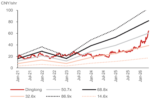
Source: Bloomberg Finance L.P., Nomura research
60
40
20
Fig. 203: Dinglong - forward P/E with -2/+2 SD
Jan-21
P/E
-1.0x SD
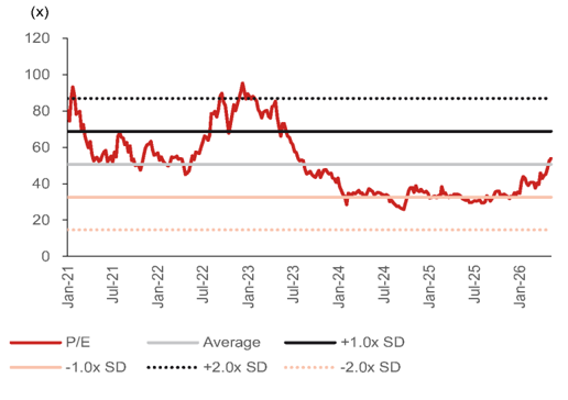
Source: Bloomberg Finance L.P., Nomura research
Relative performance chart
EQUITY: BASIC MATERIALS
Price
(CNY)
300
2751
2501
2251
200
175
1501
125
- 175
+150
F125
Anji Microelectronics Technology 688019.SS 688019 CH
EQUITY: BASIC MATERIALS
Courca. I CEC Namura
Buy on GPM recovery and sub-10nm node
Strategic thrust in sub-10nm advanced nodes and rawmaterial self-sufficiency support solid gross margins
Advanced-nodes open an incremental total addressable market
We estimate China’s CMP slurry market will scale to CNY10.5bn by 2028F, with growth concentrated in sub-10nm logic nodes, CoWoS advanced packaging, and high-layer 3D NAND/HBM - where Anji is positioned as a long-term beneficiary, in our view. Copper and copper-barrier slurries at a key client have already shifted from qualification to scaled mass production, while 7nm cobalt-interconnect slurry is advancing into customer qualification from a lead fab into a follow-on site - a greenfield category with no Cabot/DuPont (CBT US, Not rated)/(DD US, Not rated) benchmark. Advanced packaging alone adds 20% to CMP slurry demand, and Anji also anchors the broader memory portfolio. A better mix might have pushed its slurry gross margin to 55-58% in 2025 (vs. 52-55% at peers), and should continue to lift profitability as advanced-node revenue outpaces that of mature nodes.
One client’s W2W likely pivot multiple CMP steps
In addition to the sub-10nm advanced nodes development and continued raw-materials selfsufficiency, a client of Anji has been running large-scale hybrid-bonding pilots since mid-2025, pursuing an accelerated 3D DRAM roadmap that aims to narrow the gap with overseas peers, based on our industry checks. Rather than following its peers’ SoIC-style (System on Integrated Chips) die-to-die (D2D) stacking route, the client has opted for a wafer-to-wafer (W2W) hybridbonding path - conceptually closer to a packaging-level 3D DRAM via multi-die stacking seeking a non-physical-layer breakthrough through wafer/adhesive engineering that increases CMP step count, particularly pre- and post-bonding planarisation at the wafer level.
Maintain Buy on sub-10nm leadership and continued in-house abrasives
We maintain our Buy rating on Anji and lift TP to CNY360 (from CNY320). The new TP is based on 42x 2027F P/E (previously 50x 2026F P/E), which reflects: i) incremental pull-ins from growing CMP step count; ii) advanced-node exposure; and iii) ongoing in-house abrasives supporting 55-58% gross margin in 2026-28F. We raise 2026F EPS to CNY6.51 from CNY6.39 to reflect the likely gross margin recovery since 2Q26F. The stock trades at 33x 2027F P/E. Risks: ultra-high-purity silica sol remains Fuso (4368 JP, Not rated) dependent, rising competition from Dinglong (300054 CH), and fab-led vertical integration.
| Year-end 31 Dec | FY25 Actual | FY26F New | FY27F New | Old | FY28F New | ||
|---|---|---|---|---|---|---|---|
| Currency (CNY) Revenue (mn) | 2,504 | Old 3,310 | 3,310 | Old 4,137 | 4,137 | 4,965 | 4,965 |
| Reported net profit (mn) | 784 | 1,078 | 1,097 | 1,437 | 1,437 | 1,738 | 1,738 |
| Normalised net profit (mn) | 784 | 1,078 | 1,097 | 1,437 | 1,437 | 1,738 | 1,738 |
| FD normalised EPS | 4.65 | 6.39 | 6.51 | 8.52 | 8.52 | 10.31 | 10.31 |
| FD norm. EPS growth (%) | 12.3 | 37.5 | 40.0 | 33.4 | 31.0 | 21.0 | 21.0 |
| FD normalised P/E (x) | 59.5 | - | 42.5 | - | 32.5 | - | 26.8 |
| EV/EBITDA (x) | 48.2 | - | 36.5 | - | 28.9 | - | 23.7 |
| Price/book (x) | 13.2 | - | 11.0 | - | 8.8 | - | 6.9 |
| Dividend yield (%) | 0.2 | - | 0.3 | - | 0.3 | - | 0.4 |
| ROE (%) | 25.1 | 27.8 | 28.2 | 30.2 | 30.0 | 28.9 | 28.9 |
| Net debt/equity (%) | net cash | net cash | net cash | net cash | net cash | net cash | net cash |
Source: Company data, Nomura estimates
May
Global Markets Research 21 May 2026
| Rating Remains | Buy |
|---|---|
| Target price Increased from CNY 320.00 | CNY 360.00 |
| Closing price 15 May 2026 | CNY 276.80 |
| Implied upside | +30.1% |
| Market Cap (USD mn) | 7,118.6 |
| ADT (USD mn) | 145.3 |
Relative performance chart
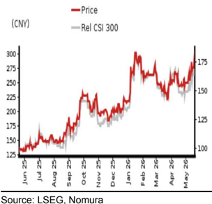
Research Analysts
Semiconductor
Frank Fan - NIHK frank.fan@nomura.com +852 2252 2195
Donnie Teng - NIHK
donnie.teng@nomura.com +852 2252 1439
Key data on Anji Microelectronics Technology
Cashflow statement (CNYmn)
| Year-end 31 Dec | FY24 | FY25 | FY26F | FY27F | FY28F |
|---|---|---|---|---|---|
| EBITDA | 715 | 992 | 1,309 | 1,642 | 1,975 |
| Change in working capital | -238 | -570 | -396 | -381 | -369 |
| Other operating cashflow | 17 | 18 | -351 | -275 | -242 |
| Cashflow from operations | 493 | 440 | 563 | 985 | 1,364 |
| Capital expenditure | -267 | -355 | -400 | -450 | -480 |
| Free cashflow | 226 | 84 | 163 | 535 | 884 |
| Reduction in investments | 0 | 0 | 0 | 0 | |
| Net acquisitions | -250 | -250 | |||
| Dec in other LT assets liabilities | -90 29 | -244 64 | 66 | 66 | |
| Inc in other LT Adjustments | -84 | -315 | 80 | 105 | 125 |
| CF after investing acts | 142 | -292 | 63 | 455 | 824 |
| Cash dividends | -58 | -88 | -123 | -160 | -194 |
| Equity issue | 28 | 857 | 0 | 0 | 0 |
| Debt | -135 | 0 | 0 | 0 | |
| issue Convertible | 173 | ||||
| debt issue Others | -20 | 381 1,015 | 35 -88 | 45 -115 | 55 |
| CF from financial acts | 123 | -139 | |||
| Net cashflow | 265 | 724 | -25 | 340 | 685 |
| Beginning cash | 633 | 898 | 1,621 | 1,596 | 1,936 |
| Ending cash | 898 | 1,621 | 1,596 | 1,936 | 2,621 |
| Ending net debt | -653 | -630 | -970 | -1,655 | |
| -655 | |||||
| Balance sheet | |||||
| (CNYmn) As at 31 Dec | FY24 898 | FY25 1,621 | FY26F 1,596 | FY27F 1,936 | FY28F 2,621 |
| Cash & equivalents Marketable securities Accounts receivable | 393 618 | 552 1,050 | 725 1,336 | 907 1,595 | 1,088 1,843 |
| Inventories Other current assets | 118 | 103 | 136 | 170 | 204 5,756 |
| Total current assets | 2,026 | 3,794 | 4,608 | ||
| 3,326 | |||||
| LT investments Fixed assets | 679 | 881 | 1,051 | 1,226 | 1,386 |
| Goodwill Other intangible | 79 | 74 | 71 | 67 | 64 |
| assets Other LT assets | 757 | 1,001 | 1,251 | 1,501 | |
| Total assets | 668 | 5,916 | 7,152 | 8,707 | |
| Short-term debt | 3,452 | 5,038 | 146 | 146 | 146 |
| Accounts payable | 130 | 146 | 244 | 300 | 357 |
| 143 | 183 | 233 | 270 | ||
| Other current liabilities | 193 | 160 | 196 586 | 773 | |
| Total current liabilities | 467 | 488 | 679 | ||
| Long-term debt | 114 | 821 | 821 | 821 | 821 |
| Convertible debt Other LT liabilities | 170 | 262 | 328 | 393 | |
| Total liabilities | 751 | 198 | 1,668 | 1,827 | |
| Minority interest Preferred stock Common stock Retained earnings Proposed dividends | 1,198 1,523 | 1,507 1,271 2,249 | 1,271 3,258 | 1,271 4,580 | 1,987 1,271 6,179 |
| Other equity and reserves Total shareholders’ equity Total equity & liabilities | -19 2,701 3,452 | 11 3,531 5,038 | -281 4,248 | -526 5,325 | -730 6,720 |
| Liquidity (x) | 8,707 | ||||
| 5,916 | 7,152 | ||||
| Current ratio | 4.34 19.4 | 6.81 - | 6.48 - | 6.79 - | 7.45 - |
| Interest cover Leverage | net cash | net cash cash | net cash cash | net cash cash | net cash |
| Net debt/EBITDA (x) Net debt/equity (%) Per share | cash | net | net cash | ||
| Reported EPS (CNY) | net | net | net | ||
| 4.14 | |||||
| 4.14 4.14 16.02 | 4.65 4.65 | 6.51 | 8.52 8.52 | 10.31 10.31 | |
| Norm EPS (CNY) FD norm EPS (CNY) | 0.34 | 4.65 20.95 0.52 | 6.51 6.51 | 8.52 31.59 | 10.31 |
| BVPS (CNY) DPS (CNY) | 25.20 0.73 | ||||
| 0.95 | 39.87 1.15 | ||||
| Activity (days) | |||||
| 78.1 | 68.9 | 70.4 | 73.5 | ||
| Days receivable | 72.0 | 299.3 | |||
| Days inventory | 295.7 | 280.7 | 303.5 | 303.2 | |
| Days payable | 68.6 | 54.9 | |||
| 54.2 | 56.2 | 57.2 | |||
| 305.2 | 294.7 | 319.8 | 315.7 | ||
| Cash cycle | 319.0 |
Source: Company data, Nomura estimates
Performance
| (%) | 1M | 3M | 12M | ||
|---|---|---|---|---|---|
| Absolute (CNY) | 9.9 | 4.5 | 101.6 | M cap (USDmn) | 7,118.6 |
| Absolute (USD) | 10.1 | 6.1 | 113.5 | Free float (%) | 47.8 |
| Rel to CSI 300 | 6.2 | 0.2 | 77.2 | 3-mth ADT (USDmn) | 145.3 |
Income statement (CNYmn)
| Year-end 31 Dec | FY24 | FY25 | FY26F | FY27F | FY28F |
|---|---|---|---|---|---|
| Revenue | 1,835 | 2,504 | 3,310 | 4,137 | 4,965 |
| Cost of goods sold | -762 | -1,084 | -1,434 | -1,764 | -2,102 |
| Gross profit | 1,073 | 1,420 | 1,875 | 2,373 | 2,863 |
| SG&A | -515 | -621 | -796 | -1,007 | -1,208 |
| Employee share expense | |||||
| Operating profit | 558 | 799 | 1,079 | 1,367 | 1,655 |
| EBITDA | 715 | 992 | 1,309 | 1,642 | 1,975 |
| Depreciation | -157 | -193 | -230 | -275 | -320 |
| Amortisation | |||||
| EBIT | 558 | 799 | 1,079 | 1,367 | 1,655 |
| Net interest expense | -29 | 10 | 33 | 21 | 25 |
| Associates & JCEs | |||||
| Other income | 39 | 40 | 77 | 175 | 210 |
| Earnings before tax | 568 | 849 | 1,190 | 1,562 | 1,889 |
| Income tax | -34 | -65 | -93 | -125 | -151 |
| Net profit after tax | 534 | 784 | 1,097 | 1,437 | 1,738 |
| Minority interests | 0 | 0 | 0 | 0 | 0 |
| Other items | |||||
| Preferred dividends | |||||
| Normalised NPAT | 534 | 784 | 1,097 | 1,437 | 1,738 |
| Extraordinary items | |||||
| Reported NPAT | 534 | 784 | 1,097 | 1,437 | 1,738 |
| Dividends | -58 | -88 | -123 | -160 | -194 |
| Transfer to reserves | 476 | 696 | 975 | 1,277 | 1,544 |
| Valuations and ratios | |||||
| Reported P/E (x) | 66.9 | 59.5 | 42.5 | 32.5 | 26.8 |
| Normalised P/E (x) | 66.9 | 59.5 | 42.5 | 32.5 | 26.8 |
| FD normalised P/E (x) | 66.9 | 59.5 | 42.5 | 32.5 | 26.8 |
| Dividend yield (%) | 0.1 | 0.2 | 0.3 | 0.3 | 0.4 |
| Price/cashflow (x) | 72.3 | 106.1 | 82.9 | 47.4 | 34.2 |
| Price/book (x) | 17.3 | 13.2 | 11.0 | 8.8 | 6.9 |
| EV/EBITDA (x) | 66.8 | 48.2 | 36.5 | 28.9 | 23.7 |
| EV/EBIT (x) | 85.7 | 59.8 | 44.3 | 34.7 | 28.3 |
| Gross margin (%) | 58.5 | 56.7 | 56.7 | 57.4 | 57.7 |
| EBITDA margin (%) | 39.0 | 39.6 | 39.6 | 39.7 | 39.8 |
| EBIT margin (%) | 30.4 | 31.9 | 32.6 | 33.0 | 33.3 |
| Net margin (%) | 29.1 | 31.3 | 33.1 | 34.7 | 35.0 |
| Effective tax rate (%) | 6.0 | 7.7 | 7.8 | 8.0 | 8.0 |
| Dividend payout (%) | 10.9 | 11.2 | 11.2 | 11.2 | 11.2 |
| ROE (%) | 22.1 | 25.1 | 28.2 | 30.0 | 28.9 |
| ROA (pretax %) | 24.1 | 26.8 | 27.9 | 28.7 | 29.3 |
| Growth (%) | |||||
| Revenue | 36.5 | 32.2 | 25.0 | 20.0 | |
| EBITDA | 38.7 | 32.0 | 25.4 | 20.3 | |
| Normalised EPS | 12.3 | 40.0 | 31.0 | 21.0 | |
| Normalised FDEPS | 12.3 | 40.0 | 31.0 | 21.0 |
Source: Company data, Nomura estimates
Company profile
Anji Microelectronics Technology (Anji), founded in 2004, is a semiconductor materials company that engages in R&D, manufacturing, selling and technology services. The company focuses on the R&D and commercialization of key semiconductor materials, and its main products include chemical mechanical planarization (CMP) slurry and photoresist solvent, which are applied in integrated circuit (IC) chips manufacturing and advanced encapsulation.
Valuation Methodology
We use P/E methodology to value Anji Microelectronics Technology. Our TP of CNY360 is based on 42x 2027F P/E, +2x SD of its historical average P/E at 26x. The target P/E is well supported by our 2025-28F earnings CAGR of 25%. The benchmark index is CSI300.
Risks that may impede the achievement of the target price
Downside risks include: 1) lackluster demand from key clients, 2) delayed expansion plans from key clients.
ESG
Anji Microelectronics Technology fits the ESG theme, as: 1) the company continues to invest in energy saving and waste recycling; and 2) obtained the Responsible Business Alliance (RBA) certificate in 2018, while issued RBA management booklet.
300
250
200
150
100
50
Fig. 204: Anji - forward P/E band
Jul-19
(X)
60
45
30
15
0
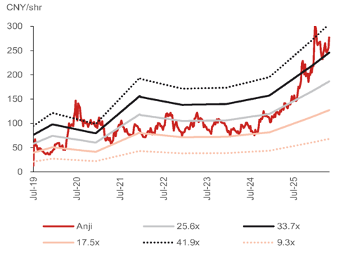
Source: Bloomberg Finance L.P., Nomura estimates
Fig. 205: Anji - forward P/E with -2/+2x SD
Jul-19
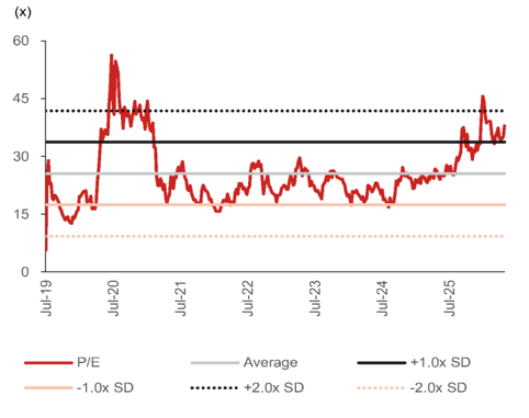
- P/E
Source: Bloomberg Finance L.P., Nomura estimates
Appendix A-1
This report has been produced by Nomura International (Hong Kong) Ltd. (NIHK), Hong Kong. See Disclaimers for Nomura Group entity details.