PDF 原檔:報告_GS_HBF高頻寬快閃記憶體_20261012_original.pdf
圖片清單(已驗證 2026-10-13)
ingest 時建立的「眼見為憑」圖片索引,是 lib/ 嵌圖的唯一真相來源。9 張全數逐張 Read(005 為 38KB,因屬 Exhibit 5 同頁圖,亦一併檢視)。
| 檔名 | size | 分類 | 親眼所見內容 |
|---|---|---|---|
報告_GS_HBF高頻寬快閃記憶體_20261012_001.png |
49KB | 真資料圖 | Exhibit 1:LLM 上下文視窗長度(token,對數座標)2020-2026 折線圖,標註 GPT-3 2K、GPT-4 8K、Claude 100K、Claude 2.1 200K、Gemini 1.5 1M/2M、Llama 4 Scout 10M(低解析度) |
報告_GS_HBF高頻寬快閃記憶體_20261012_002.png |
42KB | 真資料圖 | Exhibit 2:HBF 剖面示意圖,多層 NAND Flash Core Die 疊在 Base Die 上、以 TSV 垂直貫穿,與 GPU 並排放在同一 Interposer 上(來源 SK Hynix;低解析度) |
報告_GS_HBF高頻寬快閃記憶體_20261012_003.png |
62KB | 真資料圖 | Exhibit 3:記憶體階層散布圖,X 軸每 GB 成本(USD,對數)、Y 軸頻寬(GB/s,對數);SRAM 最右上、HBM4 約 US$25/GB、HBF 約 US$1.5/GB 且頻寬約 1,000GB/s 位於「Fast and cheap」目標區、DRAM(DDR5)、NAND SSD、HDD |
報告_GS_HBF高頻寬快閃記憶體_20261012_004.png |
111KB | 真資料圖(含財務/成本數據) | Exhibit 4 上半:HBM-only(8 顆 B200,HBM 1,536GB)vs HBM-HBF Hybrid(4 顆 B200,HBM 768GB+HBF 16,384GB)成本比較表;HBM US$15/GB、HBF US$1.75/GB、系統成本 84,000 vs 70,672、系統售價 280,000 vs 235,573(70% GM)、1M token TPS 約 10,000 vs 12,500、每 1K 輸出 token/秒成本 US$28.00 vs US$18.85、成本效率 -32.69% |
報告_GS_HBF高頻寬快閃記憶體_20261012_005.png |
38KB | 真資料圖 | Exhibit 4 下半:H3 架構 4 GPU 下,HBF 價格 US$0.25-2.50/GB 對應的成本效率增益表(-56.10% 至 -20.99%;US$1.75 為 -32.69%)熱度色階 |
報告_GS_HBF高頻寬快閃記憶體_20261012_006.png |
90KB | 真資料圖 | Exhibit 5:HBM4 vs HBF 規格比較表(容量 36 vs 512GB、價格 ~US$15.28 vs N/A、功耗 HBF 約 2-4x HBM、循序讀取頻寬 ~2.0-3.3 vs ~0.4-3 TB/s、延遲 ~20ns vs ~10μs、讀取粒度 32 vs 4096 bytes、寫入耐久 High vs Low) |
報告_GS_HBF高頻寬快閃記憶體_20261012_007.png |
56KB | 真資料圖 | Exhibit 6:SK Hynix H3 架構側視剖面圖,GPU、HBM(HBM Base+HBM Core 堆疊)、HBF(HBF Base+HBF Core 堆疊)並排於 Interposer,HBF 經 D2D 介面串接 HBM Base 與 GPU(來源 SK Hynix) |
報告_GS_HBF高頻寬快閃記憶體_20261012_008.png |
68KB | 真資料圖 | Exhibit 7:HBM-only / H3 / H3(1/2 頻寬 HBF)在 1M 與 10M token 下的標準化 TPS per batch(約 1.0 / ~1.25 / ~1.1 與 1.0 / ~6.1 / ~4.8)與 throughput per power(1M:1.0 / ~0.55 / ~0.48;10M:1.0 / ~2.7 / ~2.1)橫條圖(來源 SK Hynix) |
報告_GS_HBF高頻寬快閃記憶體_20261012_009.png |
107KB | 真資料圖 | Exhibit 8:1Q26-4Q28E 全球 NAND GB 出貨(淺藍柱,4Q28E 約 4.6e11 GB)、HBF GB(深藍小柱)與 HBF 占全球晶圓產能比重(深藍面積,右軸,4Q28E 約 9%);來源 TrendForce、GS |
OCR 備註(本檔為影像 PDF 的 OCR,以下為 ingest 時對照 PDF 原頁核對的結果)
- 首頁摘要「-$40 - $150B」為 OCR 誤判,PDF 原文為「~$40 - $150B」;首頁「50%of shipments」PDF 原文為「50% of XPUs by late 2028」。
- Exhibit 4 表格 OCR 將
B200誤為8200、TPS「10,000」誤為「000/01」;以圖檔(004)為準。 - Exhibit 9(Global HBF forecast model,PDF 第 8 頁)OCR 文字已嚴重亂碼,不可引用;以 PDF 第 8 頁為準。核對重點(4Q28E 欄):NVDA 3,588k、AMD 376k、AVGO 3,541k、MRVL 333k 單位,XPU 合計 7,838k;HBF 搭載率 50%(4Q26E 5.0%、1Q27E 10%、2Q27E 17.5%、3Q27E 25%、4Q27E 30%、1Q28E 35%、2Q28E 40%、3Q28E 45%);搭載 HBF 單位 3,919k;每單位 HBF 4,096GB;HBF 總量 16.05B GB;占全球 NAND GB 出貨 3.52%;占 SanDisk 出貨(假設 100% 市占,示意)14.43%;HBF 對傳統 NAND 晶圓空間比 3.5x、每 12 吋晶圓 HBF 37,449GB、HBF 所需晶圓 428,633 片、占全球晶圓產能 8.55%(內文與首頁寫「~9%」,表列 8.55%,圖 Exhibit 8 末端約 9%)。
- Exhibit 10 表格(個股評等與目標價)OCR 與 PDF 第 10 頁一致,無誤。
- 分析師聯絡資訊區塊 OCR 有錯字(電話、email),不影響內容;分析師姓名保留,頁面無訂閱者浮水印。
原始內容
GLOBAL TECHNOLOGY: SEMICONDUCTORS - MEMORY
High-performance NAND could help crumble the Al "memory wall" while driving meaningful CapEx savings
Key stock takeaways: We view emerging high-performance NAND-based solutions -including High-Bandwidth Flash (HBF) - as promising tools to address a worsening memory constraint in Al inference.We see a potential TAM of -$40 - $150B at a GPU adoption rate of 15%-50% by 2030 given the rapid proliferation of read-heavy and memory-intensive Al inference workloadsdespite potential challenges to adoption. We believe that HBF memory can meaningfully reduce the overall cost of inference throughput by increasing GPU utilization, resulting a-30% lower overall cost of inference throughputtranslating to as much as several hundreds of billions of hyperscaler CapEx savings.
In a bull-case scenario that assumes rapid commercial adoption of HBF on 50%of shipments - but ~9%of NANDwafer capacity given its die size penalties - similar to the HBM/DRAM dynamic.We would point out that these NAND-based solutions remain in the early development stages at a system level, and that a wide range of outcomes exists that could drive a significantly greater or smaller impact to the overall NAND supply/demand market dynamic.Steppingback, we continue to believe that limited supply additions will prolong tight NAND supply/demand in the near term - and view HBF as potentially extending the duration of the current cycle. While HBF is the technology approach thathasreceived the most attention in the technical literature, we would also highlightXL-Flash (from Kioxia) andzNAND-O (from Samsung)as alternative approaches to achieving similar objectives.
We continue to favor SanDisk (SNDK, Buy) and SK Hynix (000660.KS) given their technology leadership in HBF, and strong core business with improving product mix. We also see Samsung Electronics (005930.KS, Buy) as well positioned given its strongNAND portfolio; we see Micron (MU, Neutral)as less of a direct beneficiary given its primary focuson DRAM andlower exposure to NAND. Although we recognize challenges to widespread HBF adoption, we see promise in the technology which could drive meaningfully higher cost/performance at the system level, particularly in memory-intensive inference workloads.
James Schneider,Ph.D.
+1(2121357-2929 jim.schneider@gs.com Goldman Sachs 8 Co.LLC
Khalil Fenina
+1(212)357-6392 |khslilfenina Goldman Sachs & Co.LLC
GiuniLee
+65-6889-1025|giunilee@gs.com Goldman Sachs [Singapore) Pte
Shuhei Nakamura
|ZE66-∠85%(EIIB+ shuheinakamura@gs.com Goldman Sachs Japun Co., Ltd.
Allen Chang 882-82-2530 allen.k.chang@gs.con Goldman Sachs (Asia)LL.C.
Daiki Takayama
+81(3)4587-9870 | daikitakayama@gs.com Goldman Suchs Japun Co., Lte.
Marshall Wong
+1(646)446-0222 marshall:wong@gs.com Goldran Sachs 8 Co.LLC
Anmol Makkar +1(2121357-1366 | anmol.makkar@gs.com Goldman Sachs & Co.LLC
Luya You
+1(212)902-5297 | luya.you@gs.com Goldman Sachs I Co.LLC
Liana Wadhwani
+1212I357-3204 | liana.wadhwani@gi.com Goldman Sachs & Co. LLC
Goldman Sachs does and seeks to do business with companies covered in its research reports.As a result, investors should be aware that the firm may have a conflict of interest that couldaffect the objectivity of this report. Investors should consider this report as only a single factor in making their investment decision. For Reg AC certification and other importantdisclosures, see theDisclosure Appendix, orgo to
www.gs.com/research/hedge.html. Analysts employed by non-US affiliates are not registered/qualified as research analysts with FINRA in the U.S.
Executive Summary
On balance, we are constructive on HBF technology, and it as a promising potential solution to the intensifying memory constraint in Al inference. Our bullish view on the technology's potential is based on the following:
- Proliferation of Al inference workloads will lead to structurally higher demand for high-bandwidth, near-compute storage as context windows lengthen.
- Hs n te trr t -tntitia read bandwidth to HBMcouldresult in attractive system-level economics and accelerateadoption of HBFamonghyperscalers.
- NAND's high density of NAND, coupled with HBF's higher resulting GPU utilization, will allow the technology to command a meaningful price premium while simultaneously lowering system-level costs for hyperscalers and Al labs.
However, key challenges to adoption remain, namely latency concerns (particularly for random read /write operations), endurance and thermal considerations, and manufacturing resource intensity. Despite these challenges, we see a significant commercial opportunity in HBF and view the economics of its adoption as attractive - even at a significant price premium relative to traditional NAND.
Background -Why is there a need for High-Bandwidth Flash?
The shift to inference requires much near-compute storage capacity, and HBF's similar sequential read bandwidth vs. HBM positions it well as a potential solution to the memory constraint given NAND's high density. As more Al workflows shift away from compute-heavy training and toward memory-intensive inference, context windows are lengthening exponentially and scaling toward10 mn+ tokens from a -1.5 mn baseline (see Exhibit_1). The KV (key value) cache required for these more memory-intensive workloads is growing with larger context windows, broadly shifting the memory bottleneck from purely bandwidth-related to a combined bandwidth-capacity constraint. Although we believe DRAM-based High Bandwidth Memory (HBM) - and its subsequent iterations - islikely to lead in bandwidth and performance, the technology is significantly capacity-constrained (current architectures typically include ~192 GB per GPU) given current DRAM supply constraints.Al infrastructure operators are thus deploying additional GPU units to drive incremental compute-adjacent memory capacity, resulting in meaningfully underutilized compute capacity. Through a strategic collaboration, SanDisk and SK Hynix have introduced High Bandwidth Flash (HBF) as a proposed solution to this near-compute capacity constraint.
Exhibit 1: Chart showing context window growth over time for common LLMs
Source: Hidekazu-Konishi, data compiled by Goldman Sachs Global Investment Research
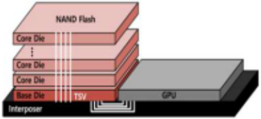
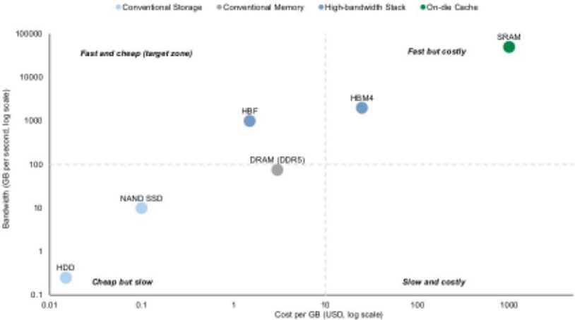
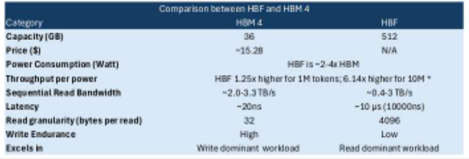
We expect HBF pricing to be significantly below DRAM-based HBM4 contract pricing (on a per GB basis) once commercial samples begin shipping in CY27 (see Exhibit 3), despite the product's pricing currently being undisclosed. High Bandwidth Flash (HBF) has been introduced an open-standard, near-compute memory tier that stacks high-density3D NAND flash into the Al accelerator package via through-silicon vias (TSVs)and UCle chiplet interconnects (see Exhibit 2). It establishes an intermediate tier in the memory hierarchy, offering a bandwidth leap over standard NANDSSDs and offers near-HBM bandwidth on a sequential read basis.Governed under the Open Compute Project (OCP)which includes SanDisk and SK Hynix, as well as ASIC customer hyperscalers (namely Alphabet and Meta), HBF delivers up to 512 GB per stack (vs. 16-32 GB per HBM stack)at sequentialread bandwidths up to-3.0 TB/s (see Exhibit 5),perthetechnical literature.
Exhibit 2: Cross-sectional architecture of High Bandwidth Flash (HBF)
Source: SK Hynix
Exhibit 3: Memory hierarchyDiagram
Source: Goldman Sachs Global Investment Research
Advantages of HBF - Cost effectiveness and other benefits
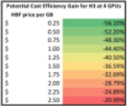
We believe HBF can lower the overall cost of equivalent inference token output by -30% or more, and lead to significant reductions in hyperscaler capital expenditures through combined hybrid architectures with HBM and increased GPU utilization.Given NAND's thermal and write endurance constraints, webelieve HBF stacks are likely to utilize SLC-based (single level cell)NANDto mitigate these risks - and given the higher costs and die size penalties will be priced far above MLC - similar to the relationshipbetween HBMand conventional DRAM.HBF's interconnect specification will likely also result in significantly lower output per wafer (given the larger physical size of an HBF chip relative to an equivalent capacity standard NAND chip; we assume HBF requires-3.5X more die/wafer area vs. traditionalNAND). Even at a meaningful premium, we see significant roomfor HBF to significantlylower inference outputcosts, even at ~1mn token context length - with thebenefit growing roughly linearly as sequences scalehigher (see Exhibit 4).
Exhibit 4: Illustrative per 1mn token cost comparison HBM only vs. H3 GPU memory architecture and HBF price per GB scenario analysis
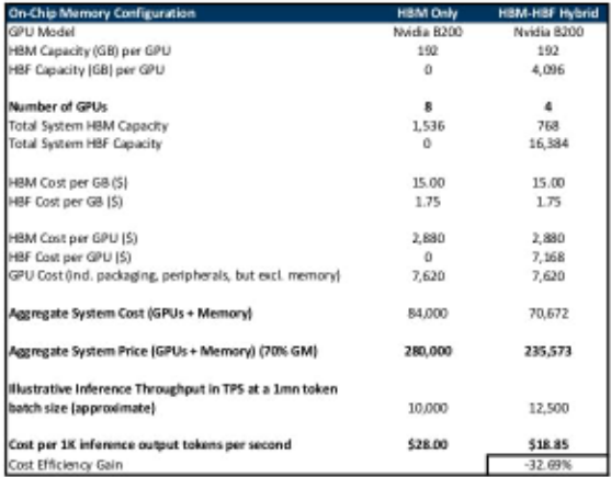
| On-Chip Memory Configuration | HBM Only | HBM-HBF Hybrid |
|---|---|---|
| GPU Model | Nvidia B200 | Nvidia 8200 |
| HBM Capacity (GB) per GPU | 192 | 192 |
| HBF Capacity (GB) per GPU | 0 | 4,096 |
| Number of GPUs | 8 | 4 |
| Total System HBM Capecity | 1,536 | 768 |
| Total System HBF Capacity | 0 | 16,384 |
| HBM Cost per GB (5) | 15.00 | 15.00 |
| HBF Cost per GB (S) | 1.75 | 1.75 |
| HBM Cost per GPU (S) | 2,880 | 2,880 |
| HBF Cost per GPU (S) | 0 | 7,168 |
| GPU Cost (ind. peckaging, peripherals,but excl. memory) | 7,620 | 7,620 |
| Aggregate System Cost (GPUs + Memory) | 84,000 | 70,672 |
| Aggregate System Price (GPUs + Memory) (70% GM) | 280,000 | 235,573 |
| Illustrative Inference Throughput in TPS at a 1mn token batch size (approximate) | 000/01 | 12,500 |
| Cost per1K inference output tokens per second | $28.00 | $18.85 |
| Cost Efficiency Gain | -32.69% |
Source: Company data, TrendForce, Goldman Sachs Global Investment Research
HBF could achieve meaningful cost advantages over HBM-only systems with higher memory density, comparable sequential read bandwidth, and higher GPU utilization.We highlight key technical points including:
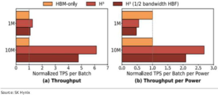
- Higher memory density: At ~512 GB per stack and ~4TB per GPU (in SK Hynix's proposed H3 architecture), HBF offers ~16X higher memory capacity vs. HBM. This density allows systems to process 2.6X larger batchsizes at1M tokens and up to 18.8X larger batches at 10M tokens compared to pure-HBM setups - resulting in serving throughput advantages widen alongside sequence length.This advantage is estimated at ~1.25X at 1 mn tokens and ~6.14X at 10 mn tokens, according to research published by SK Hynix.
- Mit D D as DRAMin peak bandwidth, research from SK Hynix and SanDisk has shown that sequential read bandwidth for HBF significantly narrows the gapwith HBMand achieves up to-3 TB/s (see Exhibit 5).Also, in most inference-heavy workloads, the number of write operations is quite limited, reducing the significance of random read or write bandwidth of memory.
- -2.7X energy efficiency gain at scale: Although an individual HBF stack consumes 2X to 4X more power in absolute terms (80–160W vs. 40W), its ability to process significantly larger inference batches may yield up to ~2.7X higher throughput-per-watt, with efficiency gains widening as context lengths scale, according to research supported bySK Hynix.
- Potential for XPU cost savings via higher utilization: By eliminating memory-capacity bottlenecks and maximizing GPU core utilization, 4 HBF-equipped XPU accelerators can potentially match the aggregate servingthroughput of an 8-XPU pure-HBM system (at192 GB / 4 TB of HBM/ HBF respectively per GPU,
accordingto SanDisk).
Exhibit 5: Comparison between HBF and HBM 4
| Comparison between HBF and HBM 4 - Category | Comparison between HBF and HBM 4 - HBM4 | Comparison between HBF and HBM 4 - HBF |
|---|---|---|
| Capacity (GB) | 36 | 512 |
| Price ($) | -15.28 | N/A |
| Power Consumption (Watt) | HBF is-2-4xHBM | HBF is-2-4xHBM |
| Throughput per power | HBF 1.25x higher for 1M tokens; 6.14x higher for 10M * | HBF 1.25x higher for 1M tokens; 6.14x higher for 10M * |
| Sequential Read Bandwidth | -2.0-3.3TB/s | -0.4-3 TB/s |
| Latency | -20ns | -10 μs(10000ns) |
| Read granularity(bytes per read) | 32 | 4096 |
| Write Endurance | High | Low |
| Excels in | Write dominant workload | Read dominantworkload |
Source: Silicon analyst, Hotchips conference, Goldman Sachs Global Investment Research
HBF's benefits are enhanced in hybrid architectures that help mitigate the
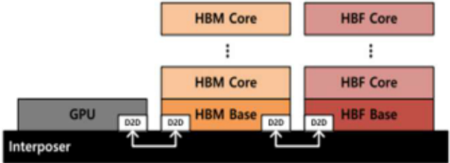
technology's keydrawbacks.Since NAND flash access latency may prove sub-optimal for real-time token generation in certain situations, SK Hynix has proposed its own"H3" architecture, which consists of a hybrid HBM-HBF configuration. The company claims this helps address NAND's write / random read bandwidth shortcomings by unifying both memory typesinto a complementary, two-tier memoryhierarchy.We note the combined architecture could potentially offer:
- ■ Zero shoreline penalty: HBF stacks are daisy-chained directly through the HBM base die, expanding on-package capacity without occupying the GPU's limited physical edge connections (see Exhibit 6)
- Optimized workload partitioning: Low-cost HBF stores massive, static data structures (model weights and pre-computed KV caches), reservingvaluable HBM capacity exclusively for latency-critical live decoding.
- Commercial and operational payoff:Offloading static memory expands concurrent batch capacity, enabling up to2.7x higher throughput per watt (see Exhibit_Z). This reduces overall GPU cluster counts and facility power draw, lowering total cost of ownership (TCO)and per-query serving costs.
Exhibit 6: Side cross sectional view of H3
Source: SK Hynix
Exhibit 7: Throughput & throughput per power comparison of HBM-only vs H3
HBF forecast model and potential commercial opportunity
We see a significant potential commercial opportunity in HBF and believe it could account for up to ~4% of global NAND bit shipments by late 2028 in a bull case that assumes a rapid and elevated adoption rate of 50% by 4Q28, which could equate to an HBF TAM of~$150 bn. In a more measured scenario that assumes a penetration rate of ~15% of GPU units bylate 2030 and a price per GB of HBF of $1.75 (which we view as conservative), we see an annualized TAM for HBF of -$40 bn.
We see HBF bits occupying up to ~9% of global NAND wafer capacity in a bull-case adoption scenario given its SLC structure and larger die size. Relative to traditional NAND, we assume a 3.5X higher wafer space usage per GB equivalent for HBF (roughly similar to the DRAM/HBM ratio) and thus see it accounting for a larger share of global NAND wafer capacity relative to its share of total NAND bits. Assuming a bull case scenario of a rapidramp in HBF's deployment to50% of GPU units by late 2028, and based on current industry forecastsfor global NAND bit output and wafer capacity, we see HBF accountingfor ~4%of global NAND bits while simultaneously consuming over 9% ofglobal NAND wafer capacity (seeExhibit 8).
Ei a l ccity
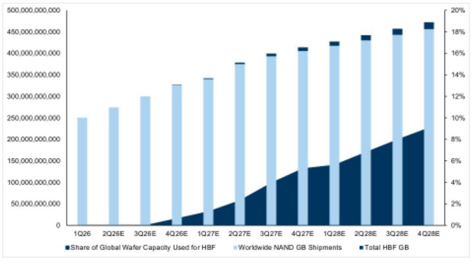
Source: TrendForce, Goldman Sachs Global Imvestment Research
Exhibit 9: Global HBF forecast model
| 100 | TH | 2,05 | 101 | alal | 1,00 | LAG | LIH | 2m 1,00 | ||||
|---|---|---|---|---|---|---|---|---|---|---|---|---|
| JMD | 4T | G8 | 444 | 8 | 8 | 141 | aa | |||||
| 3 | 10M | 1.304 | 18 | LW | 1.3m | 1.41 | ||||||
| MRM. | 1 | mH | 8 | 4 | 1m | m | I | IF | m | |||
| 1.0R | sume | 6.10 | ||||||||||
| L.00s | R | a1.00% | ||||||||||
| Ⅱ | Ⅱ | 180 | 4 | LM1 | 1094 | ten | LMm | 1.441 | 189 | |||
| iF Il pe aa | 4,00 | 4,00 | 4,00 | 4,00 | 4,00 | 40M | 4 | 4,00 | 40 | |||
| Taciner ck | 464,306,464 | 4,804,304,28 | A,00,20,8 | A,KI6,ID, | 41,06,200,(8 | 14,111,12001 | I6,NL,NA,0M | |||||
| Galal N.AD-l Shppnl | 200;004,104,184 | 28,0,, | 360) 408,000,410 6.20% | ID4,06,00,8 10.206 | 4.08% | 401,411/080,411 | 4,0,6,N0 | 441,00,306/60 | 404,20,M8,140 | |||
| 6.12% | AMS 0.17% | 14% | 13% | L3% | 1.00% 1.8/% | 1.00% 1.19% | 357 | |||||
| 0.00% #,a0,408, | 1041880+11 | Laamv1L | LADAIHII | LAHGI | 1.111800+11 | |||||||
| 100% morkat dort) | 80,142; M4,084 0.m | 8mS | 00m | 1.1m | 1.8 | 3.3m9 | 4.3m | 8.8 | 8.8N | 108m% | 11.am | 34.45 |
| alul vtalerlarts in/sa | 4,011,000 | 4,004,000 | 1,80, | 4,001,000 | 4,18,I | 4,2II | 4,20,000 | 4,711,300 | ||||
| Mx TH. NANe- . m | SRURE | uum | SRURE | SRUE | SRURE | uume | ||||||
| CEW+O% GN BA R. | 13 | 13s | 1.5 | 13 | 13s | 35 | 13s | 13 | ||||
| Mx iF pe Llis Waler | 11,400 | 11,480 | 0,408 | 11,400 | 80,408 | 10,408 | 11.40 | 11,400 | 10,408 | 11.,408 | 11,400 | |
| Wulers liealal for Her | 244,A0K | |||||||||||
| ihail le Ha | 0.m | R.mS | 00m | 1.m8 | 1m% | s.ms | S.8IN | 10m | tars | 8.505 |
Source: TrendForce, Goldman SachsGlobal Investment Research
Challenges to HBF adoption
Despite the promise of High-Bandwidth Flash, we note several key challenges to adoption.
- Bandwidth constraints and latency concerns: According to SanDisk, SK Hynix, and other studies, HBF offers comparable sequential read bandwidth to HBM4, although
8
- we note that (1)HBM4E is currently in the sampling phase and delivers at least ~50% higher bandwidth; (2)although inference workloads are read-dominant overall, any write operations significantly reduces the effective bandwidth of HBF given its NAND-based design; (3)HBF's structurally lower write performance and endurance relative to DRAM-based HBM results in its practical benefits being highly dependent on its read performance keeping pace with the latest generations of HBM.
- Variability of read/write ratio in inference: As context windows expand and workloads shift to read-heavy inference, occasionalwrite operations in KV cache remain essential: if no prefix cache hit occurs (i.e., the prompt /prefix is not found in the existingKV cache), the read/write ratio is effectively zero. Although this ratio will likely become increasingly rareover time and inference remainshighly read-dominant, the variability of write operation frequency (and the resulting meaningful bandwidth penalty for NAND-based HBF) could render the effective bandwidth of HBFunpredictable in the early phases of any rollout.
- Endurance, energyintensity, and thermal concerns: Because it is based on NAND flash, HBF tolerates a finite number ofprogram/erase cycles - whereas DRAM-based HBMoffers far greater write endurance. Also, the higher density of a HBF cube result drives higher energy consumption per stack (-160 W per cube in SK Hynix's H3 architecture, ~4X more power than HBM3E vs.~2.5X more power than HBM4). Given the peak power of most flagship accelerators of ~1,000-1,200 W, and the utilization of 8 HBF stacks in H3, the power footprint of HBF alone can easily approach the accelerator's own constraints and result in new thermal issues. This excess heat may further accelerate wear on the flash cells and complicate lifespan considerations.
- Manufacturing resource intensity: As with HBM, HBF uses design changes to maximize bandwidth, including increased internal structuralparallelism and 3D packaging methods. It also uses ultra-wide on-package interconnect to alleviate the external data bottleneck. These advanced packaging techniques, the use of hybrid bonding, and the ultra-wide interconnect all contribute to a more resource-intensive and higher-cost manufacturing process, including a significantly higher wafer consumption (most estimates suggest a 3X-4X higher cost relative to traditional NAND, similar to the DRAM/HBM "trade ratio").
In aggregate, we view HBF's potential bandwidth limitations and resource intensity as the most significant challenges facing wide adoption of the technology. As context windows lengthen and the share of inference workflows grows, we see improved visibility on the read/write ratio in KV cache and on pricing as key variables.
Alternative approaches to scaling the memory wall- XL Flash and zNAND-0
We are constructive on the broad set of NAND-based technologies set to address memory constraints in Al inference - and see alternative approaches such as XL Flash and zNAND-O ultimately driving similar implications.While HBF remains one of the leading approaches to addressing current Al system memory constraints given public backing from SanDisk and SK Hynix (and ongoing development from Samsung) and significant peer-reviewed publications, other approaches have emerged, including
"XL Flash."Introduced by Kioxia and built on the company's BiCS Flash 3D NAND architecture, the approach includes key architectural and design differences relative to HBF which could potentially offer easier packagingintegration and/or lower cost, potentially at the expense of some performance. We would also highlight Samsung's development of zNAND-O - similar in concept such as using TSV to connect 4 or 8 layer vertical stacks of V-NAND dies, while targeting a different market segment in on-device Al (smartphones, PCs, etc.).Samsung is alsodevelopingzHBM for data centers where it stacks the memory on top of the Al accelerator rather than next to it, to improve the performance and power efficiency. Although it is too early to tell which approach might come to market first, we believe that all three approaches areultimately aimedat solving the "memory wall" problem by applying NAND-based system approaches to increase context length while offering significant potential cost savings at the system level.
XL flash may hold write, cost, and certain other advantages over HBF, although based on publicly-available literature HBF appears well-suited for read-heavy Al inference applications.XL Flash utilizes standard PCle, NVMe, and CXL system buses, but relies on less dense SLC-basedNAND, smaller transfer blocks, andlarger die architectures relative to traditional 3D NAND flash to maximize bandwidth, significantly lower random read latency, and meaningfully increase write endurance; characteristics that may render XLFlash better suited for write operations relative to HBF.The technology's reliance on existing approaches to 3DNAND manufacturing, its lack of TSVs (through-silicon vias, required for the stacking associatedwith HBF), andphysical separation from the GPU (vs. HBF using the same silicon interposer)may also lower the upfront transition costand perceived investment risks.
Individual stock implications:
Exhibit 10: Select stocks within our coverage positioned to be affected by HBF
| Company | Ticker | Rating | 12monthpricetarget | Current Price | Upside/ downside |
|---|---|---|---|---|---|
| Advanced Micro Devices | AMD | Buy | $700 | $611 | 14.5% |
| Broadcom | AVGO | Buy | $540 | $363 | 48.9% |
| Kioxia | 285A.T | Buy | ¥38,667 | ¥17,505 | 120.9% |
| Micron | MU | Neutral | $1,250 | $1,027 | 21.7% |
| Nvidia | NVDA | Buy | $300 | $229 | 30.7% |
| Samsung | 005930.KS | Buy | W500,000 | W262,000 | 90.8% |
| Sandisk | SNDK | Buy | $2,200 | $1,607 | 36.9% |
| SK Hynix | 000660.KS | Buy | W3,500,000 | W1,681,000 | 108.2% |
Note: Current Price is as of October 9, 2026.
Source: Goldman Sachs Global Investment Research
- SanDisk (SNDK, Buy): We remain constructive on SNDK and view the company as a well-positioned beneficiary of the potential widespread adoption of HBF given its technologyleadership in collaboration with SK Hynix and its low capital intensity through itsKioxia manufacturing partnership- which we see as particularly differentiating given the resource intensity of HBF. We alsobelieve the company can simultaneously retain its solid core business in traditional NAND, which we expect to continue to outperform on improving product mix and further progress on its BiCS roadmap.
10
- Kioxia Holdings (285A.T, Buy): We reiterate our Buy rating on Kioxia given our expectations on ongoing supply shortages in the NAND market and constructive pricing outlook, which we believe should lead to positive street estimate revisions. We also believe Kioxia is poised to announce a series of shareholder return, including the resumption of dividend payment as well as continued share buyback. Regarding XL-Flash, which isintended to expand the memory capacity of GPUs in inference GPU servers, Kioxiaplans to ship samples of a product achieving over 10 million IOPS (storage processing speed) by the end of CY26. It also plans to ship samplesof a second-generation product with processing speed further increased to 100 million IOPS in CY27. Compared to HB Flash (HBF), Kioxia'sSSD-based solution is differentiatedin that it does not require additional manufacturing processes such as TSV.
- SK Hynix(000660.KS,Buy): We maintain our positive view on Hynix and see the company asa potential leader inthe HBF market. While the company's focus remains on higher-margin DRAM and HBM, Hynix is uniquely positioned to be a prime beneficiary ofHBF market expansion given its proactive initiatives in co-development and industry standardization of HBF with SanDisk. Through leveragingits advancedNAND technology, vast experience in producing various types of NAND, and the advanced packaging expertise from HBMleadership, we believe Hynix possesses the core competencies required for HBF commercialization.
- ■I Samsung Electronics (005930.KS, Buy, on CL): We maintain our Buy rating(on the APAC Conviction List) on SEC. AlthoughSEC has not yet releasedspecific details on its work on HBF (although it did recently file a trademark application for "zHBF"), recent announcements on its technology milestones—such as the TSV-integrated zNAND-Oarchitecture—demonstrate its active R&D in high-bandwidthNAND. Supportedby its largest NAND capacity globally and technologyleadership, we believe SEC will likely be ready to compete in the high-bandwidth NAND market, also leveragingits superior cost management and packaging competitiveness. We highlight SEC being the only company in the world that can produceDRAM and NAND while having the foundry/logic/advanced packaging capabilities, which we believe along with the industry's largest memory capacity (for both DRAM and NAND), will help the company to continue to lead across an increasingly multi-tiered Al memoryhierarchy.
- Micron (MU, Neutral): While we expect the company to participate in any significant future HBFmarket, we view its focus on HBM andDRAM, its lack of participation in the consortiumgoverningHBF, and its prioritization of DRAM greenfield capacity overall as likely to temper its potential future market share in the novel NAND technology.We are Neutral-rated on MU, primarily on the risks of HBM pricing momentum slowing in 2028given the prospects of meaningful supply additions by the industry, as well as possible de-specing of HBMas HBF adoption ramps.We nevertheless see continued tailwinds for Micron's business overall, but view SK Hynixand SanDisk as more direct and nearer-termbeneficiaries ofany HBF-related inflection in NAND demand.
- Semi Cap Equipment: We view HBF as a modest incremental positivefor semiconductor equipment demand, though the implications are more nuanced than
a simple increase in NAND content. On one hand, HBF introduces additional manufacturing complexity through TSVs, hybrid bonding, advanced packaging, inspection, and test, which could benefit equipment suppliers with exposure to packaging and integration workflows. On the other hand, HBF's value proposition is rooted in reducing memory capacity bottlenecks andimproving GPU utilization, which could ultimately lower the number of accelerators required for a given inference workload. We nevertheless see the added packaging, integration, and memory intensity as likely to offset any reduction in system-level hardware demand.
- Digital Semis: We see an incrementally negative impact for a range of XPU accelerator makers, includingNvidia, Broadcom, AMD, and others - as the success of any high-performance NAND approach is likely to reduce the number of accelerators ultimately deployed at a similar performance level given the potential cost savings involved.We would point out that Nvidia is currently the only provider of accelerators which controls the entire system stack from software to hardware components - and hence it may be able tooptimize the system-level design to mitigate this impact, similar to what it has done by optimizing the HBM-NAND balance in the current Rubingeneration.
12