PDF 原檔:產業_SEMICON2026矽光子論壇_UMC簡報_20260831_original.pdf
原始內容
Breaking through the DCI data rate barrier
Wenchi Ting, Ph. D. Vice President Corporate Technology Office UMC
Outline
- 1 | Bandwidth scaling laws
- 2 | Challenges from higher data rates
- 3 | Modulator selection
- 4 | Coherent technology comes to rescue?
- 5 | WDM vs single wavelength
- 6 | Summary
UMC
Copyright © UMC
2
Is there a data rate scaling law equivalent to Moore's law for CMOS scaling?
- You bet there is. In fact there are two such laws I managed to find.
- Edholm's Law of Bandwidth: Telecommunication bandwidth doubles approximately every 18 months.
- Nielsen's Law of Internet Bandwidth: Bandwidth capacity roughly doubles every 21 months.
- What does this mean for DCI's (data center interconnects): Roughly every a year and a half to two years, the capacity/module doubles.
| bandwidth capacity | peak market adoption |
|---|---|
| 10G to 40G | 2018~2022 |
| 100G | 2020~2024 |
| 400G | 2023~2026 |
| 800G | 2025~2028 |
| 1.6T and beyond | 2025+ |
per Gemini
Challenges from higher data rates
- In this presentation we focus on the scaling trend of DCI's date rate/channel, not per module, and on the photonic part of the transceivers.
- Critical components in an electrical-optical transceiver:
- The modulator
- The DSP/SERDES
- EIC: TIA and driver
- The photo diode
- 200 Gbps/channel already happened. The most common configuration:
- PAM4
- Si MZM (DFB laser)
- Ge PD
- SiGe BiCMOS TIA/driver
- Advanced logic DSP/SERDES
- IM/DD, single-wavelength
- 400 Gbps/channel in demo status, facing many challenges, as almost every component seems shaky at such data rate.
- Si modulators out of steam
- Ge PD bandwidth very marginal
- Bipolar transistors need to reach 500 GHz f T for TIA/driver
- DSP/SERDES extremely difficult to design
Courtesy of Cisco
UMC
Can this scaling trend go on forever?
- The scaling trend is not likely to continue in a brute-force manner. Both electronics and optics face stiff challenges at 400 Gbps/channel and above.
- SERDES facing CMOS performance limitation.
- On optical side both photo diodes and Si modulators face bandwidth limitations.
- 400 Gpbs/channel (PAM4) requires > 110 GHz electrical 3-dB bandwidth!
- 300 Gbps/channel a 'bridging' data rate spec
- Paths to higher data rates (400 Gbps/channel and above):
- PAM4 -> PAM8
- Adopting components with higher bandwidth
- Coherent transmission
- WDM: multiple wavelengths per channel
- A combination of the above
Modulator selection
- Modulator - maybe the most critical device of the photonic technology.
- Si and SiGe modulators:
- MZM:
Courtesy of Photonic Spectra
Table 1. State-of-the-art high bandwidth all-silicon MMs.
| structure | BW (GHz) | Vr (V) | BWN* (GHZV) |
|---|---|---|---|
| segmented drive [11] | 67 | 5 | 13.4 |
| substrate removed + 35 S load [14] | 60 | 7 | 8.6 |
| low load impedance [12] | 47 | 5.4 | 8.7 |
| microring-assisted MZMs [13] | 67 | 7.5 | 8.9 |
| distributed micro-capacitors [1] | 61 | 8.3 | 7.3 |
| doping optimization [15] | 67 | 5 | 13.4 |
| conventional [10] | 44 | 8 | 5.5 |
| conventional [16] | 41 | 7 | 5.9 |
| slow light waveguide |9] | 110 | 78 | 1.4 |
| transparent electrodes (This work) | 168 | 7 | 23 |
| transparent electrodes (This work) | 140 | 28 |
Modulator selection
- MRM:
Jayatilleka et al., Intel, 2022
UMC
- Small foot print
- Low drive voltage
- High intrinsic electrical bandwidth (due to low resistance)
- Extremely sensitive to temperature
- Demanding on process control
- Trading off extinction ratio against speed
- Not a promising candidate for 400 Gbps/channel and above
Modulator selection
- SiGe EAM:
Verbist et al., J. Lightwave Technology, 2016
Courtesy of Gemini
| Feature | SiGe EAM | MZM |
|---|---|---|
| Footprint | Very small (~ 50 μm) | Large (millimeters) |
| Drive Voltage | Low (~ 1V - 3V) | High |
| Energy Efficiency | High (fJ/bit range) | Moderate |
| Optical Bandwidth | Narrow (wavelength specific) | Wide (broadband) |
| Chirp / Dispersion | High (can cause penalty over distance) | Lower than SiGe EAM |
| Primary Use Cases | Short-reach data centers, AI tensor cores, on-board optical transceivers | Long-haul telecom, coherent optical networks, high-power applications |
Modulator selection
- Other candidates:
- InP EML (laser+EAM) and MZM
- Thin-film LiNbO 3 (TFLN) MZM
- Organic
- Graphene
- Thin-film LiTaO 3
- …
- InP and TFLN are the two most promising solutions, as these are much more mature than the other contenders.
TFLN modulators
- UMC Group's TFLN program started on 2021.
- 6' in mass production, 8' in sampling
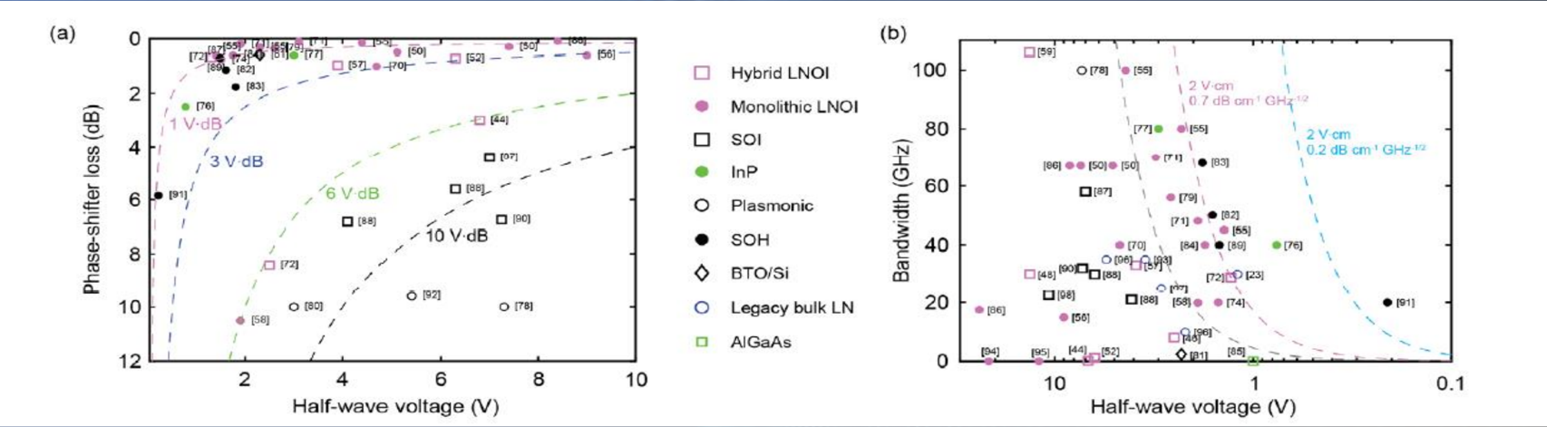
- LiNbO3 's excellent optical and E/O properties coupled with mature TFLN substrate infrastructure (up to 8' in substrate size) making TFLN the leading modulator candidate for 400 Gbps/channel and above.
Zhang et al ., Optica, 2021
TFLN pros and cons
- Strengths: low loss, high bandwidth (> 110 GHz), good thermal stability, superb linearity.
- Weaknesses: large, expensive (compared with Si), integration with SiPh requiring either heterogeneous integration or advanced packaging.
Kharel et al ., Optica 2021
Copyright © UMC
TFLN is here to stay
- InP facing severe shortage, adding to TFLN's momentum.
- TFLN the best modulator solution for Coherent Lite given its superb linearity. It is the best solution for 400 Gbps/lane IMDD too.
- Integrating TFLN with PIC is a challenge as well as an opportunity. This is in hot pursuit.
- Advanced packaging schemes and micro transfer printing are both promising candidates.
- UMC is developing the integration technology, leveraging our expertise in PIC, TFLN, and advanced packaging.
- Rather diverse applications of TFLN are being explored, across a number of wavelengths. Innovations taking advantage of LiNbO 3 's unique optical properties are happening at an unexpected pace. This is perhaps only the tip of the iceberg.
Ge Photo Diodes
- Good enough for 200 Gbps (bandwidth ~ 50+ GHz) but marginal at 400 Gbps/channel (110+ GHz).
- May still make it to 400 Gbps/channel with process/layout/design optimization.
- High uncertainty whether Ge PD can ever go beyond 400 Gbps.
- InP very expensive and harder to integrate.
- Alternative materials being explored: GeSn, SiSn, etc., but still early on the learning curve .
Coherent technology comes to the rescue?
- Traditionally, coherent technology was used for telecom only, not for datacom.
- Expensive, bulky, and energy hungry.
- Modulating amplitude, phase, and polarization.
- Carrying huge data load over very long distances.
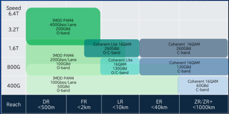
- Coherent Lite is now entering datacom as a viable solution for :
- Connecting servers that could be a Km away within the same data center.
- Providing relief to the bandwidth challenge.
- Additional optical loss (~ 3 dB) from OCS helps justify Coherent Lite over IM/DD.
- Coherent Lite could be different from a telecom coherent technology:
- O-band
- Shorter reach (2~20 Km)
- Single polarization
- Hardware simplified
- Lower power
- Lower cost
Coherent technology comes to the rescue?
https://techtimes.dexerials.jp/en/photonics/coherent-lite-pic/
https://fundaai.substack.com/p/deepcoherent-lite-reshapes-ai-optical
WDM
- Squeezing multiple 's into the same channel.
- DWDM (8 or more 's/fiber) and CWDM (fewer than 8 's/fiber).
- Actively pursued for scale-up CPO applications to handle the large amount of electronic channels.
- Multiple single- lasers are easier to implement but comb-lasers may be a better solution in the long run due to better power efficiency.
So what is likely to happen at 400 Gbps and beyond, for DCI?
- Adoption of higher-performance modulators (TFLN/InP) and improvement in photo diodes are key factors affecting deployment of plain-vanilla (non-WDM, IM/DD) DCI's with 400 Gbps/channel performance and beyond.
- A combination of WDM, PAM8, and even coherent transmission may be more 'elegant' solutions than brute-force bandwidth scaling. And these are being actively pursued.
- The scaling law in DCI's data rate/channel is likely to slow down as transceivers becoming more complicated to enable WDM and coherent coding schemes, and/or to incorporate non-Si (TFLN, InP) modulators.
- As a result, future connectivity scaling will increasingly rely on heterogeneous integration and advanced photonic platforms, rather than brute-forcing wider bandwidth from each component.
Conclusion
- Winning solutions for future DCI need to be balanced in cost and performance, likely leveraging optical components made by different materials and integrated together seamlessly through advanced packaging schemes.
[讀者資訊已遮蔽] [讀者資訊已遮蔽]
Thank you!
圖片清單(已驗證 2026-10-23)
逐張 Read 驗證(≥40KB 者)。
p12/p17為整頁渲染圖(文字頁),非資料圖。
| 檔名 | size | 分類 | 親眼所見內容 |
|---|---|---|---|
產業_SEMICON2026矽光子論壇_UMC簡報_20260831_001.png |
87KB | 真資料圖 | LightCounting 光模組銷售額堆疊長條圖(2024–2030,速率別 25G 至 3.2T,標註 800G、1.6T 兩處箭頭) |
產業_SEMICON2026矽光子論壇_UMC簡報_20260831_002.png |
225KB | 真資料圖 | 光電收發器方塊圖(Courtesy of Cisco):Transmitter(Driver/Modulator/Clock Data Recovery/Equalization)、Receiver(TIA/LA/Pre-emphasis/Output driver)、Photodiode、Fiber array coupling interface、Laser source、Micro-controller,並區分電子元件(綠)與光子元件(藍) |
產業_SEMICON2026矽光子論壇_UMC簡報_20260831_003.png |
60KB | 真資料圖 | Si MZM 結構:上為 1×2 MMI/p-n 相位移器/2×1 MMI 俯視示意,下為行波電極(Ground/Signal/Ground)與 n-Si/p-Si 波導剖面 |
產業_SEMICON2026矽光子論壇_UMC簡報_20260831_004.png |
351KB | 真資料圖 | 微環調變器(MRM,Intel 2022)立體結構:Ge implant、PD bias、pn junction、V heater、Tungsten、Via 等圖例 |
產業_SEMICON2026矽光子論壇_UMC簡報_20260831_005.png |
216KB | 真資料圖 | SiGe EAM 剖面(n-i-p,GeSi 600 nm 寬、300 nm 厚,摻雜濃度色階)與 C-band 元件尺度 100 µm 示意(Verbist, JLT 2016) |
產業_SEMICON2026矽光子論壇_UMC簡報_20260831_006.png |
328KB | 真資料圖 | SiGe EAM vs MZM 比較表(Footprint、Drive Voltage、Energy Efficiency、Optical Bandwidth、Chirp/Dispersion、Primary Use Cases) |
產業_SEMICON2026矽光子論壇_UMC簡報_20260831_007.png |
359KB | 真資料圖 | 各調變材料平台散點圖(Zhang, Optica 2021):左為相位移器損耗 vs 半波電壓,右為頻寬(GHz)vs 半波電壓;圖例 Hybrid/Monolithic LNOI、SOI、InP、Plasmonic、SOH、BTO/Si、Legacy bulk LN、AlGaAs |
產業_SEMICON2026矽光子論壇_UMC簡報_20260831_008.png |
213KB | 真資料圖 | TFLN MZM 示意(Optical signal/RF signal 行波電極與參數 h、w 標示,右上標 TFLN MZM) |
產業_SEMICON2026矽光子論壇_UMC簡報_20260831_009.png |
53KB | 真資料圖 | 灰階電鏡影像(標 (b)),為 TFLN 調變器電極區截面/俯視圖,無文字說明 |
產業_SEMICON2026矽光子論壇_UMC簡報_20260831_010.png |
92KB | 真資料圖 | TFLN 調變器立體示意((c)(d) 兩組電極結構,LN 波導與金電極,光斑標示) |
產業_SEMICON2026矽光子論壇_UMC簡報_20260831_011.png |
21KB | 真資料圖 | TFLN 波導剖面((e):LN、SiO2、Au,Quartz 基底,標 h、w0、s、g) |
產業_SEMICON2026矽光子論壇_UMC簡報_20260831_012.png |
98KB | 真資料圖 | 速率×傳輸距離應用地圖:縱軸 400G/800G/1.6T/3.2T/6.4T,橫軸 DR<500m/FR<2km/LR<10km/ER<40km/ZR/ZR+<1000km;IMDD PAM4(100G/lane 50GBd、200G/lane 100GBd、400G/lane 200GBd,O-band)、Coherent Lite 16QAM(130GBd、260GBd,O/C-band)、Coherent 16QAM(60/130/260GBd,C-band)各占區塊 |
產業_SEMICON2026矽光子論壇_UMC簡報_20260831_013.png |
71KB | 真資料圖 | 相干收發架構:Tx 為雷射→MZM I/MZM Q→3dB coupler→SP-QAM(QPSK/16QAM);Rx 為 PBS/Pol-Folding→Hybrid→BPD→TIA→ADC→DSP,含 LO |
產業_SEMICON2026矽光子論壇_UMC簡報_20260831_014.png |
211KB | 真資料圖 | WDM 示意:四個 Data Channel 不同波長(紫/青/綠/紅)經 Optical coupler 合入單一光纖 |
產業_SEMICON2026矽光子論壇_UMC簡報_20260831_p12.jpg |
137KB | 文字卡 | 第 12 頁整頁渲染:「TFLN is here to stay」四點條列(內容已在原始內容文字中) |
產業_SEMICON2026矽光子論壇_UMC簡報_20260831_p17.jpg |
144KB | 文字卡 | 第 17 頁整頁渲染:結論條列(內容已在原始內容文字中) |