PDF 原檔:報告_MS_科技供應鏈_20260706_original.pdf
圖片清單(已驗證 2026-07-07)
ingest 時建立的「眼見為憑」圖片索引,是 lib/ 嵌圖的唯一真相來源;嵌入時只從這裡挑分類為「真資料圖」的,不照 trimmed 引用順序猜。建立步驟見
ingest_steps.mdStep 2.5。
| 檔名 | size | 分類 | 親眼所見內容 |
|---|---|---|---|
260706_ms_tech-supply-chain_012.png |
45KB | 真資料圖 | CPO 封裝結構示意圖:Switch/XPU 疊 Substrate,其上為 PIC/EIC 疊層;右側箭頭指向「FOCI's ReLFACon™」實物 |
260706_ms_tech-supply-chain_001.png |
65KB | 裝飾·logo·banner | Asia Summer School 2026 泳池橫幅廣告 |
260706_ms_tech-supply-chain_004.png |
83KB | 真資料圖 | ABF 基板供需趨勢圖 2015–2030E:藍色柱供給量、米色柱需求量(T mm²),綠色折線供需比(>100% = 缺貨),2028 年後需求缺口加速擴大 |
260706_ms_tech-supply-chain_002.png |
93KB | 真資料圖 | MS 研究覆蓋亞洲科技供應鏈彙整表:CoPoS(TSMC/Ibiden/Innolux)、ABF 基板+TPU(Nitto Boseki/Ibiden/Unimicron/Nan Ya PCB/Zhen Ding/SEMCO/MediaTek/TSMC)、CPO+FAU(TSMC/FOCI/Suzhou TFC/ASE),含代號、分析師、評等 |
260706_ms_tech-supply-chain_003.png |
132KB | 真資料圖 | ABF 基板供應鏈流程圖:Nittobo(T-Glass)→ Ajinomoto(ABF 絕緣膜)→ Ibiden / Unimicron / Nan Ya PCB / Zhen Ding / Samsung SEMCO(ABF 基板)→ TSMC(先進封裝)→ MediaTek(IC 設計)→ Google(超大型雲端客戶) |
260706_ms_tech-supply-chain_011.png |
134KB | 真資料圖 | CPO 封裝截面圖:FAU/OE 含 EIC/PIC 透過 μbump 連接 GPU/Switch Interposer,含 Hybrid bonding pad、Bump、Substrate、BGA Ball、PCB 完整封裝堆疊 |
260706_ms_tech-supply-chain_005.png |
137KB | 真資料圖 | CoPoS 面板尺寸效益比較:300mm wafer(7 interposers,面積效率 ~45%)vs 300×300mm² panel(16 interposers,~81%,降本 ~10%)vs 600×600mm² panel(64 interposers,~81%,降本 ~20%) |
260706_ms_tech-supply-chain_006.png |
198KB | 真資料圖 | 有機基板與玻璃核心基板結構對比圖:左側有機基板(傳統 PCB-like woven glass laminate core)vs 右側玻璃核心基板特性說明(低損耗、高密度 TGV、CTE 接近矽) |
260706_ms_tech-supply-chain_007.png |
240KB | 真資料圖 | 玻璃核心基板面板實物照片:藍色手套持拿大片面板,顯示黃橙色基板圖案及面板尺寸 |
260706_ms_tech-supply-chain_008.png |
213KB | 真資料圖 | 封裝後晶片實物照:多顆藍色封裝晶片排列於黑色托盤,藍色手套觸碰其中一顆 |
260706_ms_tech-supply-chain_009.png |
246KB | 真資料圖 | TGV(Through Glass Vias)掃描電子顯微鏡照片:俯視 TGV 陣列及 500μm 尺度下截面放大結構 |
260706_ms_tech-supply-chain_010.png |
519KB | 真資料圖 | Corning GlassBridge Fiber-to-PIC Connector 產品規格文件:含 IOX 波導特性說明、24+ 光纖支援、可回焊、低損耗(1.5dB O-band),及 NPO/CPO 架構支援示意圖 |
原始內容
M July 6, 2026 02:20 AM GMT
Asia-Pacific Technology | Asia Pacific
Connecting Dots in Tech Supply Chain: CoPoS, T-Glass/TPU, Glassbridge/FAU
TSMC has reportedly pulled forward CoPoS to address Intel EMIB-T competition. MediaTek TPU volumes have upside after securing Japan T-Glass. Taiwan's CPO supply chain development remains on track; Glassbridge seems remote at this stage.
What's new? Investors are asking how we reconcile views and research from tech supply chain analysts, which may sometimes look inconsistent. Last year's most popular example was upstream CoWoS capacity-implied chips vs. AI server rack consumption ( link ). We try to connect the dots here.
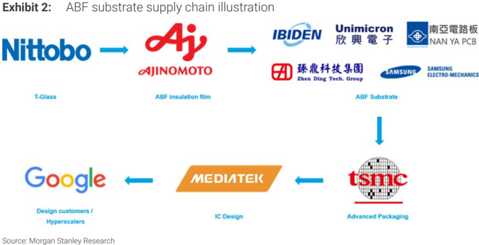
- T-Glass shortage vs. TPU volume upside: MediaTek gets more T-Glass supply from Japan for its 3nm Google TPU project . In MediaTek: Upside in both cloud and edge chip business; OW (23 Jun 2026) , we noted that MediaTek can assist Google (covered by Brian Nowak) in sourcing more T-Glass from the Japanese fiber material vendor to secure supply. Hence, we see upside to our shipment and revenue assumptions for 3nm ZebraFish TPU - we now forecast 3mn units in 2027. The question here is - how can MediaTek source even more T-Glass supply?
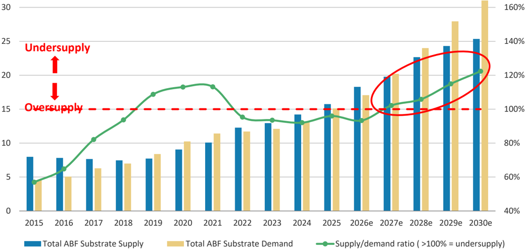
Our Japan manufacturing analyst, Yoshihito Hasegawa, believes that Nitto Boseki, which he covers, is the leading T-glass supplier for Google's TPU. According to our hardware analyst, Howard Kao, Zhen Ding is likely MediaTek's key second source for 3nm TPU substrates alongside Unimicron. However, Howard believes Zhen Ding's primary value drivers are its exposure to China AI chip ABF substrates, optical transceiver module PCBs, and AI server PCBs rather than TPUs ( Zhen Ding: Strong preliminary May profits [22 Jun 2026]) . See Howard's analysis of CoWoS capacityimplied substrate demand vs. ABF substrate supply gap ( Exhibit 3 ).
- TSMC CoPoS pulled forward? According to news reports , TSMC's CoPoS will collaborate with Ibiden (covered by Shoji Sato) for substrates, and with Innolux (covered by Derrick Yang) focusing on TGV (Through Glass Vias) for Nvidia's Feynman GPU. TSMC guided that CoPoS mass production should be from 2028/2029. Glass core substrates are critical to large reticle size chips, mainly but not limited to the CoPoS packaging (meaning it can be used for large CoWoS packaging as well), although our checks indicate that glass core substrate and CoPoS do not have to be adopted at the same generation of GPU.
(continued...)
| Morgan Stanley Taiwan Limited+ Charlie Chan Equity Analyst | +886 2 2730-1725 |
|---|---|
| Charlie.Chan@morganstanley.com Morgan Stanley Asia Limited+ Andy Meng, CFA Equity Analyst Andy.Meng@morganstanley.com | +852 2239-7689 |
| Morgan Stanley Taiwan Limited+ Derrick Yang Equity Analyst Derrick.Yang@morganstanley.com Howard Kao Equity Analyst Howard.Kao@morganstanley.com | +886 2 2730-2862 |
| Morgan Stanley MUFG Securities Co., Ltd.+ Yoshihito Hasegawa | +886 2 2730-2989 |
| Equity Analyst Yoshihito.Hasegawa@morganstanleymufg.com | +81 3 6836-8910 |
| Shoji.Sato@morganstanleymufg.com Morgan Stanley & Co. International plc+ Shawn Kim Equity Analyst Shawn.Kim@morganstanley.com Morgan Stanley Taiwan Limited+ | +81 3 6836-8404 |
| Tiffany Yeh Equity Analyst | +44 20 7677-1018 |
| Tiffany.Yeh@morganstanley.com Daniel Yen, CFA Equity Analyst | +886 2 7712-3032 +886 2 2730-2863 |
| Daniel.Yen@morganstanley.com Morgan Stanley Asia Limited+ Daisy Dai, CFA Equity Analyst | |
| Daisy.Dai@morganstanley.com | +852 2848-7310 |

Morgan Stanley does and seeks to do business with companies covered in Morgan Stanley Research. As a result, investors should be aware that the firm may have a conflict of interest that could affect the objectivity of Morgan Stanley Research. Investors should consider Morgan Stanley Research as only a single factor in making their investment decision.
For analyst certification and other important disclosures, refer to the Disclosure Section, located at the end of this report.
+= Analysts employed by non-U.S. affiliates are not registered with FINRA, may not be associated persons of the member and may not be subject to FINRA restrictions on communications with a subject company, public appearances and trading securities held by a research analyst account.
M
From our foundry supply chain checks, CoPoS could be adopted in the Feynman Ultra in 2029, while the first generation Feynman in 2028 would use TSMC's 3D stack (die to wafer) for GPU stacking with SiC carriers to assist with chip thermal management. The key question is whether TSMC will bring forward the CoPoS timeline for Feynman in 2028.
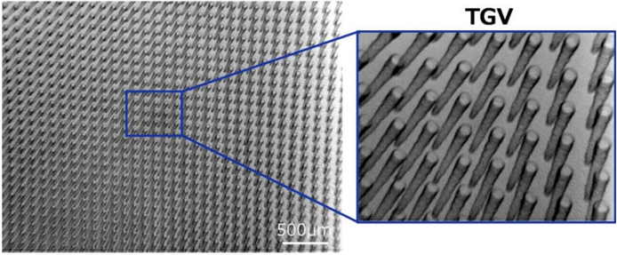
According to Derrick Yang (Greater China - Displays: Progress for Glass in Advanced Packaging among Panel Makers [29 Jun 2026]), we do see the potential of glass panels in semiconductors, as the package size gets bigger - though a more realistic timing for HPC adoption looks to be 2028/2029. Innolux will conduct the TGVs (Through Glass Vias) process on a glass panel (510mm*515mm), before sending that to Ibiden for substrate processes. For Innolux, the challenges lie in forming TGVs and the subsequent copper plating, because this is not part of the regular display panel production. Our understanding is that Innolux will need to procure new equipment for glass cores. The major CoPoS fab will be TSMC AP7 (see Exhibit 5 ), located in Tainan, Taiwan, close to Innolux's factory. Innolux's TGV production is likely to be in 2028, and we see a small chance of early adoption at Feynman.
Howard Kao, who covers Greater China substrate names, indicated there could be more substrate vendors apart from Ibiden to supply the glass core substrates in future. We believe the major technology bottleneck is the TGV process given glass scrap issues; again, we think 2029 is more likely timing for CoPoS.
- GlassBridge to replace or complement to FAU in CPO? Fiber Array Units (FAU) are used to connect the optical fibers to the optical engines around the networking chips. According to our hardware analyst Andy Meng's report, Greater China Technology Hardware: GlassBridge and Fiber -to -PIC's Implications for AI Transceiver and FAU Makers (28 Jun 2026), Corning GlassBridge is a fiber to PIC connector platform that brings optical fiber directly to a photonic integrated circuit (PIC). For AI transceiver companies (e.g. Eoptolink, covered by Andy), the impact should be limited as GlassBridge can be used in both CPO and NPO. However, GlassBridge adoption timing remains to be seen, along with whether it would complement FAU based approaches by offering a wafer based, passively aligned alternative.
According to our semiconductor analyst, Tiffany Yeh (see her latest report, link), we do not rule out that GlassBridge could hamper FAU's TAM in the long run, but we are yet to see any projects in TSMC's COUPE platform that have adopted this technology. On the other hand, GlassBridge mainly serves edge coupling, and can only currently support one -dimension fiber layouts. However, TSMC's mainstream COUPE platform and key customers' solutions, such as NVIDIA, AMD (both covered by Joseph Moore), and Ayar Labs, are still sticking to grating coupling for the next few years, as it is easier to achieve mass production - which we expect in 2H26. Lastly, CPO requires integrated design and discussion across the whole ecosystem - including foundry (OE), chip designer, FAU, laser, and even system integrator - so it is hard to change a design overnight. GlassBridge is an ideal solution but we believe it remains far from mass production. We see TSMC scaling PIC capacity to 25kwpm in 2028, with Ins2 test efficiency improving. We stay overweight on CPO enablers, as investor expectations are already on the floor.
Mol suvolale supply chant mustatul!
→
IBIDEN
M
NAN YA PCB
ELECTRO-MECHANICS
Connecting Dots in Asia Tech - Key Exhibits
Design customers /
Hyperscalers
MEDIATEK
IC Design
Unimicron
Exhibit 1: Key Asian supply chain companies under our coverage
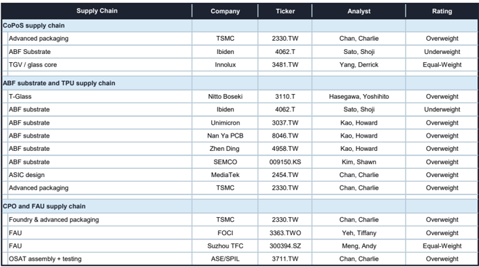
| Supply Chain | Company | Ticker | Analyst | Rating |
|---|---|---|---|---|
| CoPoS supply chain | ||||
| Advanced packaging | TSMC | 2330.TW | Chan, Charlie | Overweight |
| ABF Substrate | Ibiden | 4062.T | Sato, Shoji | Underweight |
| TGV / glass core | Innolux | 3481.TW | Yang, Derrick | Equal-Weight |
| ABF substrate and TPU supply chain | ||||
| T-Glass | Nitto Boseki | 3110.T | Hasegawa, Yoshihito | Overweight |
| ABF substrate | Ibiden | 4062.T | Sato, Shoji | Underweight |
| ABF substrate | Unimicron | 3037.TW | Kao, Howard | Overweight |
| ABF substrate | Nan Ya PCB | 8046.TW | Kao, Howard | Overweight |
| ABF substrate | Zhen Ding | 4958.TW | Kao, Howard | Overweight |
| ABF substrate | SEMCO | 009150.KS | Kim, Shawn | Overweight |
| ASIC design | MediaTek | 2454.TW | Chan, Charlie | Overweight |
| Advanced packaging | TSMC | 2330.TW | Chan, Charlie | Overweight |
| CPO and FAU supply chain | ||||
| Foundry & advanced packaging | TSMC | 2330.TW | Chan, Charlie | Overweight |
| FAU | FOCI | 3363.TWO | Yeh, Tiffany | Overweight |
| FAU | Suzhou TFC | 300394.SZ | Meng, Andy | Equal-Weight |
| OSAT assembly + testing | ASE/SPIL | 3711.TW | Chan, Charlie | Overweight |
Source: Morgan Stanley Research
M
Exhibit 3: Expecting ABF substrate under-supply gap to widen by 2030 vs. our prior estimates
T mm²
Source: Morgan Stanley Research (e) estimates.
Exhibit 4: Increased demand assumptions causing CY29-30 under-supply gap to widen vs. our prior estimates
| ABF SD | 2026e | 2027e | 2028e | 2029e | 2030e |
|---|---|---|---|---|---|
| Old | 96.6% | 102.6% | 106.8% | 112.2% | 114.6% |
| New | 93.3% | 102.2% | 105.8% | 114.9% | 122.3% |
Source: Morgan Stanley Research (e) estimates.
M
Overview of Technologies discussed in this Report
CoPoS
Chip-on-Panel-on-Substrate (CoPoS) is an emerging TSMC technology aimed at scaling package size and reducing cost: By moving toward panel-level or large-area RDL-based packaging, CoPoS enables much larger integration footprints beyond the reticle limits of silicon interposers. This makes it attractive for next-generation AI systems that require integrating many large dies. Its advantages lie in scalability and potential cost efficiency at large sizes, but it is less mature than CoWoS and offers lower interconnect density. As such, it is not yet ideal for the most bandwidth-critical interfaces, and is still evolving in terms of ecosystem and manufacturability.
However, given the recent needs of larger sizes of chip design, and competition from Intel (covered by Joseph Moore), we believe the schedule for TSMC CoPoS could be pulled forward earlier to 2028, in the hope of meeting the needs of those GPU or AI ASICs adopting 2nm process or below.
Exhibit 5: TSMC's advanced packaging fab planning
| Advanced Packaging Plant | Location | Focused Technology |
|---|---|---|
| AP1 | Hsinchu | R&D |
| AP2 | Tainan | Bumping |
| AP3 | Taoyuan | InFOandWMCM |
| AP5 | Taichung | CoWoS |
| AP6 | Miaoli | SoIC |
| AP7 | Chiayi | WMCM, CoWoS, SoIC, CoPoS |
| AP8 | Tainan | CoWoS |
| AP9 and AP10 | Arizona | SoIC/CoWoS/CoPoS/WMCM/R&D |
Source: Company data, Morgan Stanley Research
Exhibit 6: Comparison between TSMC's CoWoS, CoPoS, SoIC, and Intel's EMIB-T
| CoWoS | CoPoS | SoIC | EMIB | |
|---|---|---|---|---|
| Packaging solutions | 2.5D Wafer level | 2.5D Panel level | 3D Chip/die stacking | 2.5D Substrate level |
| Performance (data bandwidth) | High | Low | Highest | Low |
| Efficiency for large chip (use of the subrate area) | Low | High | NA | High |
| Production sweet spot of the chip size | <9.7x reticle size | >9.7x reticle size | >9.7x reticle size | >9.7x reticle size |
| Cost at 9.7x retical size (including yield issue) | High | Theoretical low | Highest | Theoretical low |
| Technology maturity (opposite of execution risk) | High | Low | Medium | Low |
| Thermal challenge | Medium | Theoretical low | Highest | Theoretical low |
| Overview | CoWoSexcels in high-bandwidth 2.5D integration but is costly and capacity- limited | CoPoS targets large-scale, cost- efficient integration but is still maturing | SoIC delivers the highest performance through 3Dstacking at the expense of complexity and thermal constraints | EMIB offers a more cost-effective and modular alternative with some performance trade-offs |
| Strategic consideration from customers | Strategic consideration from customers | Strategic consideration from customers | Strategic consideration from customers | Strategic consideration from customers |
| Pros | Reliable and time to market | Cost efficient with larger chip size | Breakthrough the planar constraints | Cost efficient with larger chip size |
| Cons | Higher Cost | Not currently avaiable atTSMC | High cost with thermal issue | Execution Risk |
Source: Morgan Stanley Research
O YOLE
Group
COMPARISON OF WLP AND PLP
M
Size does matter!
-10% cost decrease
300x300mmª panel
16 interposers
Area efficiency -81%
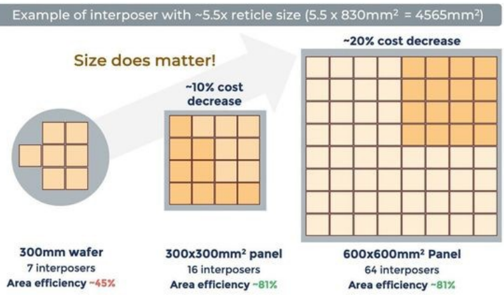
Exhibit 7:
CoWoS, CoPoS and FoPLP comparison
600x600mm? Panel
64 interposers
Area efficiency -81%
Source: Yole
Glass Core Substrates
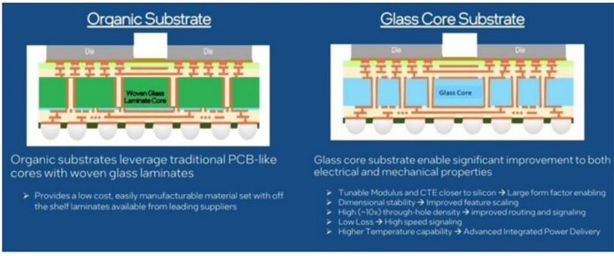
Though the ultimate goal of glass-core substrates is to support multiple high-performance computing chips, they can also serve applications with less demanding specifications. Therefore, before glass sees adoption as an interposer in advanced packaging, we believe it could gain traction as a substrate core, replacing the conventional resin and glass-cloth composite core used in select high-end organic substrate applications. This should not be interpreted as glass cloth becoming obsolete. We expect glass-core adoption to be gradual, while mainstream ABF and other organic substrates should continue to rely on glass-cloth-reinforced resin cores in the near term.
Glass has several advantages over organic cores, including:
- Fine line width/space and via pitch: Down to 2um in line width/space, 75um on via pitch can accommodate more I/Os for more chips with more complex functions (50% more dies on a chip) or reduce the metal layers
- Higher bump density: Die-to-die bump pitch is less than 35um on substrate to reduce die area and power consumption
- High speed I/O: Smooth copper interconnects, ultra low-loss dielectric and fine TGV pitch together can enable high speed transmission at lower cost vs. optical solutions
- Better mechanical strength : Less warpage and distortion amid elevated temperatures during the packaging process
- Similar CTE as chips: Less mismatch of coefficient of thermal expansion (CTE) can mitigate the warpage issue
300mm wafer
7 interposers
Area efficiency -45%
ІтІ Ег 111 С ||
Oldso uule vuvollate vo. Haultullal Ulyalle vuvotate
Organic Substrate
Glass Core Substrate
TGV
M
Organic substrates leverage traditional PCB-like cores with woven glass laminates
> Provides a low cost, easily manufacturable material set with off
500
the shelf laminates available from leading suppliers
Exhibit 8: Glass Core Substrate vs. Traditional Organic Substrate
electrical and mechanical properties
Dimensional stability → Improved feature scaling
Source: Intel
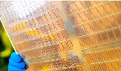
Exhibit 9: Glass Core Substrates in Panel Form
Source: Intel
CAmoll O.
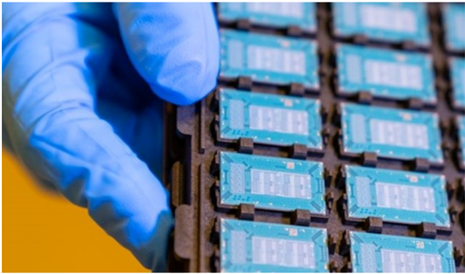
Exhibit 10: Packages with Glass Core Substrates
Source: Intel
Exhibit 11: TGV on Glass Core Substrate
Source: DNP
Glassbridge/FAU
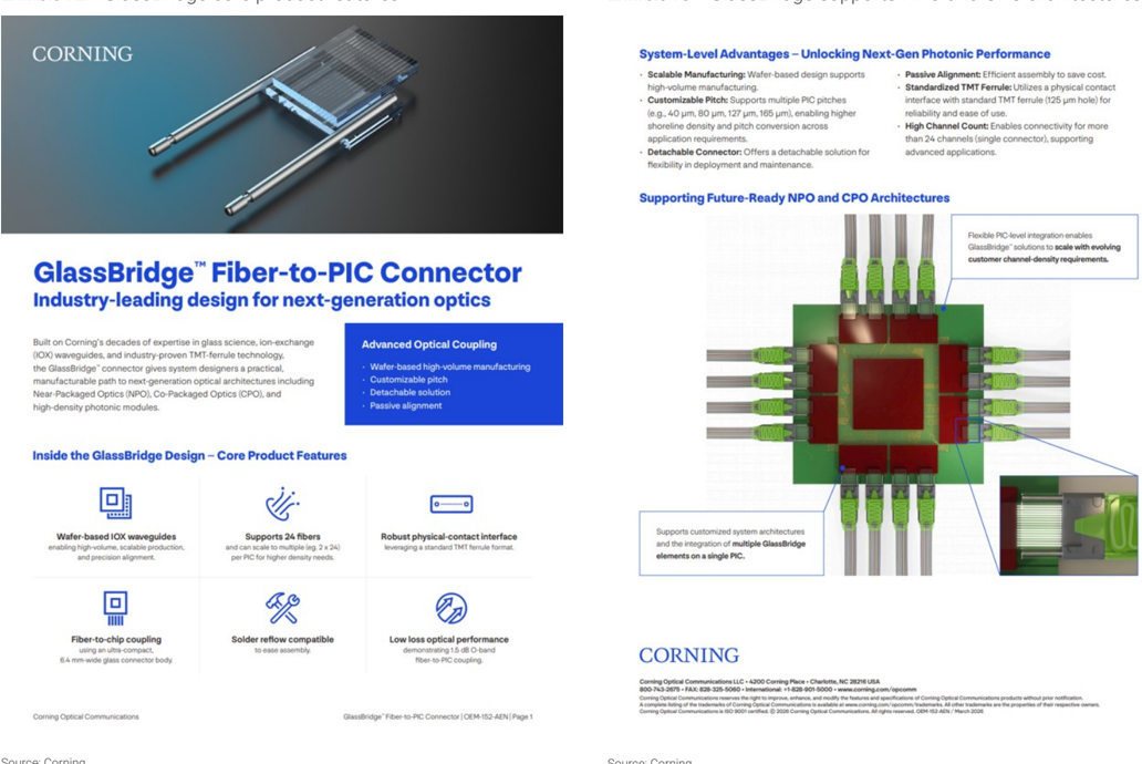
On June 24, Corning (covered by Meta Marshall) officially launched its GlassBridge glass optical interconnect assembly at the AI Data Center Optical Communications and Interconnect Technology Conference held in Seoul. Based on Corning's document:
1) Corning GlassBridge is a fiber -to -PIC connector platform that brings optical fiber directly to a photonic integrated circuit (PIC).
NINAON
M
as so esee pee cineen.
suonesiaoe pasuene
2) Fiber -to -PIC technology refers to the optical interface that couples optical fiber directly into a PIC rather than through a long fiber assembly.
3) Traditional Fiber Array Units (FAU) become complex to assemble and scale at very high fiber counts. GlassBridge complements FAU -based approaches by offering a wafer -based, passively aligned alternative that supports higher density, improved scalability, and detachable system integration.
In CPO development, FAU makers are likely to face disruption risk with GlassBridge emerging as a new technology approach. For AI transceiver companies, the impact should be limited as GlassBridge can be used in both CPO and NPO. Wider application in NPO could potentially offset CPO risk.
Exhibit 13: GlassBridge supports NPO and CPO architectures
Source: Corning sepinoanen ool peseo-1e
mognios eigeneee.
sieqy 7z stioddns
Exhibit 12: GlassBridge core product features
Source: Corning
siodons oisen paseo ialel ..r mim .
seoloe moisann pon pee pese meneon stueweinber mone ..
Uulllo ulm mmetyusel
FOCI'S
M
Bump
BGA Ball
Substrate
РСВ
-l..A
V.. 1
A.aA TIAAALII
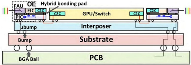
Exhibit 14:
"Optics on Interposer"
Source: Song, S., Mehta, N., Nedovic, N., Rekhi, A., Kalogerakis, G., Xu, L., … Gray, C. T. (2026). A 32Gb/s/λ 256Gb/s/Fiber Half-Rate BandpassFiltered Clock-Forwarding DWDM Optical Link in a 3D-Stacked 7nm EIC/65nm PIC Technology.
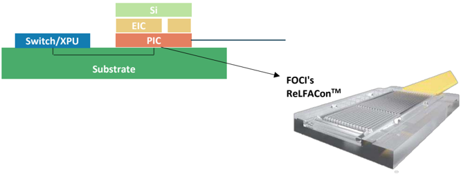
Exhibit 15: ReLFACon enables direct transmission of external photonic signals with MCM modules to achieve reliable signal transmission
Source: FOCI
0 0
M
Disclosure Section
The information and opinions in Morgan Stanley Research were prepared or are disseminated by Morgan Stanley Asia Limited (which accepts the responsibility for its contents) and/or Morgan Stanley Asia (Singapore) Pte. (Registration number 199206298Z) and/or Morgan Stanley Asia (Singapore) Securities Pte Ltd (Registration number 200008434H), regulated by the Monetary Authority of Singapore (which accepts legal responsibility for its contents and should be contacted with respect to any matters arising from, or in connection with, Morgan Stanley Research), and/or Morgan Stanley Taiwan Limited and/or Morgan Stanley & Co International plc, Seoul Branch, and/or Morgan Stanley Australia Limited (A.B.N. 67 003 734 576, holder of Australian financial services license No. 233742, which accepts responsibility for its contents), and/or Morgan Stanley Wealth Management Australia Pty Ltd (A.B.N. 19 009 145 555, holder of Australian financial services license No. 240813, which accepts responsibility for its contents), and/or Morgan Stanley India Company Private Limited having Corporate Identification No (CIN) U22990MH1998PTC115305, regulated by the Securities and Exchange Board of India ('SEBI') and holder of licenses as a Research Analyst (SEBI Registration No. INH000001105); Stock Broker (SEBI Stock Broker Registration No. INZ000244438), Merchant Banker (SEBI Registration No. INM000011203), and depository participant with National Securities Depository Limited (SEBI Registration No. IN-DP-NSDL-567-2021) having registered office at Altimus, Level 39 & 40, Pandurang Budhkar Marg, Worli, Mumbai 400018, India; Telephone no. +91-22-61181000; Compliance Officer Details: Mr. Tejarshi Hardas, Tel. No.: +91-22-61181000 or Email: tejarshi.hardas@morganstanley.com; Grievance officer details: Mr. Tejarshi Hardas, Tel. No.: +91-22-61181000 or Email: msic-compliance@morganstanley.com which accepts the responsibility for its contents and should be contacted with respect to any matters arising from, or in connection with, Morgan Stanley Research, and their affiliates (collectively, "Morgan Stanley"). Morgan Stanley India Company Private Limited (MSICPL) may use AI tools in providing research services. All recommendations contained herein are made by the duly qualified research analysts.
For important disclosures, stock price charts and equity rating histories regarding companies that are the subject of this report, please see the Morgan Stanley Research Disclosure Website at www.morganstanley.com/eqr/disclosures/webapp/generalresearch, or contact your investment representative or Morgan Stanley Research at 1585 Broadway, (Attention: Research Management), New York, NY, 10036 USA.
For valuation methodology and risks associated with any recommendation, rating or price target referenced in this research report, please contact the Client Support Team as follows: US/Canada +1 800 303-2495; Hong Kong +852 2848-5999; Latin America +1 718 754-5444 (U.S.); London +44 (0)20-7425-8169; Singapore +65 6834-6860; Sydney +61 (0)2-9770-1505; Tokyo +81 (0)3-6836-9000. Alternatively you may contact your investment representative or Morgan Stanley Research at 1585 Broadway, (Attention: Research Management), New York, NY 10036 USA.