產業_SEMIVISION_3D堆疊SRAM_20260520
PDF 原檔:產業_SEMIVISION_3D堆疊SRAM_20260520_original.pdf
原始內容
substar
Beyond HBM Why 3DStacked SRAM Is Becoming Critical to AI Processor Architecture
Original Article By SemiVision Research Reading time: 23mins]
From Node Scaling to System Scaling: Why Semiconductor Process Technology Is Becoming Application-Driven
For decades, the semiconductor industry was defined by one dominant question: who could move to the next process node first? From 90nm to 28nm, from 7nm to 5nm, and now toward 3nm and 2nm, the industry’s competitive logic appeared straightforward: smaller geometry
© 2026 TSMC, Ltd.
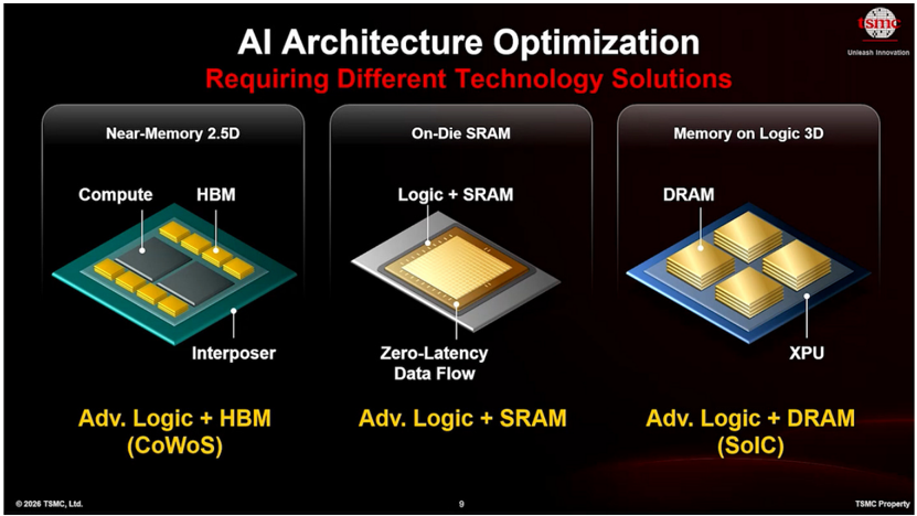
Al Architecture Optimization
Requiring Different Technology Solutions
Near-Memory 2.5D
Compute
On-Die SRAM
Memory on Logic 3D
meant higher density, lower power, better performance, and stronger pricing power. Logic + SRAM DRAM
But that logic is no longer sufficient.
The next phase of semiconductor competition is not simply about shrinking transistors. It is about matching the right process, the right packaging architecture, the right reliability standard, and the right power-performance profile to the right application. Smartphones, AR glasses, electric vehicles, autonomous driving systems, and robots are no longer asking for the same type of chip. Each application has its own physics, cost structure, thermal envelope, safety requirement, and system architecture. This is why the industry is moving from nodecentric scaling to application-driven system scaling.
The End of the One-Node-Fits-All Era
Advanced nodes remain critical. N5, N4, N3, and the coming N2 generation continue to define the cutting edge for mobile SoCs, AI accelerators, and high-performance computing. These nodes deliver higher transistor density, better energy efficiency, and stronger sme
Unleash Innovation performance per watt. For smartphones and AI devices, that still matters enormously. However, not every function benefits equally from the newest node. A mobile SoC may need a 3nm CPU or NPU, but its RF subsystem, image signal processor, power management IC, display driver, embedded memory, and sensor interface may be better served by mature or specialty processes. In automobiles, the central ADAS processor may migrate to 5nm, 3nm, or eventually 2nm, but microcontrollers, radar chips, CIS sensors, power devices, and battery management ICs will remain distributed across 28nm, 22nm, 16nm, BCD, RF, CIS, SiC, and GaN platforms. This is the key structural shift: the future semiconductor platform is no longer a single monolithic node, but a heterogeneous system assembled from multiple process technologies.
Smartphones: The Original Driver of Advanced Logic Scaling
The smartphone remains one of the most demanding semiconductor platforms in the world. A modern mobile SoC integrates CPU cores, GPU blocks, ISP engines, 5G modems, Wi-Fi connectivity, DSPs, NPUs, memory controllers, security modules, and power management interfaces into a highly constrained thermal and battery envelope. This is why mobile chips have historically been among the earliest adopters of advanced foundry nodes. The move from 7nm to 5nm, and then to 3nm, gave smartphone chip designers more transistors within the same die area while reducing energy consumption. For mobile devices, every milliwatt saved can become longer battery life, better sustained performance, thinner form factors, or more room for AI inference. But even in smartphones, the industry is moving away from a purely monolithic model. Advanced logic may sit on N3 or N2, while RF, analog, image processing, memory, and connectivity blocks may be manufactured on different optimized nodes. Over time, packaging technologies such as InFO, 3D integration, and chiplet-based architectures will allow smartphone platforms to become more modular.
The implication is clear: future mobile performance will not come only from a smaller transistor. It will come from process partitioning, advanced packaging, memory proximity, thermal design, and system-level power management.
AR Glasses: Why Display Drivers Are Becoming Semiconductor Strategy
AR and VR devices introduce a different challenge. Unlike smartphones, near-eye displays must operate under extreme size, weight, heat, and power constraints. The display subsystem cannot simply consume more power, because heat is directly perceived by the user. It cannot occupy large board area, because the device must fit into glasses. It cannot tolerate slow response, because latency affects user comfort.
This is why high-voltage display driver technology is becoming strategically important.
TSMC’s N16HV process is an important signal. By introducing highvoltage capability into a FinFET platform, the display driver can become smaller, more power-efficient, and more suitable for OLED and near-eye display systems. According to the source material, N16HV offers higher gate density and lower power compared with N28HV, while also reducing chip area and power consumption for near-eye display applications.
This is not just an incremental display driver improvement. It suggests that AR glasses may require a new class of semiconductor platform: one that combines display driving, sensing, wireless communication, edge AI, and power management in a form factor closer to consumer electronics than traditional computing.
In other words, smart glasses will not be won by optics alone. They will be won by the semiconductor companies that can solve display power, sensor fusion, edge inference, thermal control, and miniaturized packaging at the same time.
The Next Frontier of AI in Consumer Tech: AR Glasses
SEMIVISION · NOVEMBER 6, 2025 Read full story
Automotive: Advanced Nodes Meet Long-Lifecycle Reliability
Automotive semiconductors follow a different logic from consumer devices. A smartphone chip may be replaced every two to three years. A car platform may need to operate for more than a decade. This means automotive chips must satisfy long product lifecycles, wide temperature ranges, functional safety requirements, and strict reliability
At the same time, electric vehicles and autonomous driving systems are pushing automotive chips toward much higher compute intensity. ADAS and autonomous driving require real-time perception, sensor fusion, AI inference, and centralized decision-making. This is why the automotive architecture is moving from many distributed ECUs toward central compute and zonal control.
TSMC’s N2A automotive process reflects this direction. Based on the source text, N2A applies nanosheet transistor technology to automotive applications and is expected to support higher performance at the same power level versus N3A, with AECQ100 qualification targeted standards such as AECQ100. around 2028.
The deeper message is that automotive semiconductors are no longer only about mature nodes. They are splitting into two layers.
The first layer is the high-performance compute layer: ADAS SoCs, autonomous driving processors, AI accelerators, and centralized vehicle computers. These will increasingly adopt advanced nodes such as N5A, N3A, and eventually N2A.
The second layer is the control, sensing, power, and reliability layer: MCUs, radar, CIS, battery management, gate drivers, power ICs, and SiC/GaN modules. These will remain on specialized and mature process platforms.
The car of the future is therefore not a single semiconductor market. It is a multi-process, multi-package, safety-certified computing system on wheels.
NVIDIA Automotive: Smarter Cars, Bigger Responsibility
SEMIVISION · MAR 11 Read full story
Robotics and Physical AI The Next Edge Computing Platform
Robotics may become one of the most important semiconductor growth vectors after smartphones and EVs. Unlike cloud AI, robotics requires intelligence to be embedded inside a physical machine. The robot must see, listen, feel, infer, decide, move, and correct itself in real time.
This is why the concept of Physical AI matters. A robot is not merely an AI model with motors attached. It is a closed-loop control system that must integrate sensors, actuators, edge processors, motor controllers, wireless links, power devices, safety mechanisms, and real-time software.
The source material emphasizes that next-generation robots require local AI processing, low-latency deterministic control, sensor fusion, and reliable communication between sensors, actuators, and central compute units. This creates a very different semiconductor demand profile from traditional industrial automation. A humanoid robot or service robot may need: CPU and NPU cores for AI inference; vision processors for cameras and depth sensors; radar or LiDAR interfaces for navigation; MCUs for motion control; power devices for actuators; wireless modules for connectivity; and secure processors for safety and identity. The robot is therefore a semiconductor system that combines the characteristics of a smartphone, an electric vehicle, an industrial controller, and an AI edge server. This is why robotics will likely accelerate demand for heterogeneous integration rather than a single
dominant node.
FinFET to GAA The Transistor Is Still Important, But It Is No Longer Alone
The transition from FinFET to Gate-All-Around nanosheet transistors remains one of the most important technology shifts in advanced logic. FinFET improved electrostatic control by wrapping the gate around three sides of the fin. But as scaling moves below 3nm, variability, leakage, and drive current optimization become more difficult. GAA nanosheet transistors improve gate control by surrounding the channel more completely. They also allow transistor drive current to be tuned by adjusting nanosheet width, giving designers more flexibility in balancing performance and power. For high-performance computing, AI, and premium mobile SoCs, this transition is critical. But the transistor is no longer the only bottleneck.
Power delivery, interconnect resistance, thermal density, memory bandwidth, packaging warpage, and signal integrity are becoming equally important. That is why backside power delivery is emerging as another important scaling technology. By moving power delivery to the backside of the wafer, chip designers can reduce IR drop, free up front-side routing resources, and improve power efficiency in highly dense logic designs. more precise: transistor scaling is becoming one component of system
The conclusion is not that transistor scaling is ending. The conclusion is scaling.
Advanced Packaging: The New Scaling Layer
As the cost and complexity of advanced nodes rise, advanced packaging becomes the bridge between process technology and system architecture. CoWoS, InFO, chip-on-wafer, 2.5D integration, 3D stacking, hybrid bonding, and chiplet architectures allow designers to combine multiple dies fabricated on different process nodes. This is especially important because different functions have different optimal nodes. Logic may require N2 or N3. SRAM may scale differently. Analog and RF may not benefit from the newest node. Power devices may require entirely different materials. Sensors may need specialized process modules. Advanced packaging allows the industry to avoid forcing all functions onto one expensive monolithic die. Instead, it enables a more efficient partitioning of the system. This is why advanced packaging is no longer a back-end manufacturing service. It is becoming a front-line architecture platform. The companies that control heterogeneous integration will increasingly shape the performance, cost, and scalability of future AI, automotive, AR, and robotics systems.

The Cost Wall: Why Specialty Processes Matter More
The economics of advanced nodes are becoming more severe. A leading-edge 3nm chip can require enormous design investment, complex IP qualification, expensive EDA flows, longer validation cycles, and higher mask costs. Not every application can absorb this cost.
This is why specialty processes are becoming more valuable. Highvoltage FinFET for display drivers, embedded MRAM or FeRAM for edge devices, BCD for power management, RFSOI for wireless, CIS processes for image sensors, SiC and GaN for power electronics, and automotive-qualified logic platforms all represent different forms of process differentiation.
The future is not simply ‘more advanced’ or ‘more mature.’ The future is more specialized.
For foundries, this means that process leadership will be measured not only by the smallest node, but also by the breadth of platforms they can offer. For chip designers, it means the key question is no longer ‘Which node is the most advanced?’ but ‘Which combination of nodes and packages creates the best system?‘
Strategic Outlook: The Semiconductor Industry Is Becoming a System Industry
The next decade of semiconductor competition will be shaped by four structural forces.
- First, advanced logic will remain essential for AI, mobile, and highperformance computing. N3, N2, and future nanosheet/CFET architectures will continue to define the performance frontier.
- Second, specialty processes will expand because every application has different physical constraints. AR needs low-power highvoltage display drivers. EVs need automotive-grade reliability and power semiconductors. Robots need real-time edge AI and deterministic control. Sensors need photonic, RF, MEMS, or imaging-specific platforms.
- Third, advanced packaging will become the true system integration layer. Chiplets, 2.5D, 3D stacking, and heterogeneous integration will allow the industry to combine advanced and mature nodes inside one optimized system.
- Fourth, cost and reliability will become as important as density. The best semiconductor solution will not always be the smallest node. It will be the architecture that delivers the right balance of performance, power, area, cost, reliability, and manufacturability.
Conclusion: The Real Race Is No Longer Nanometers, But System Fit
The semiconductor industry is entering a new phase. The old race was about shrinking the transistor. The new race is about matching process technology to system architecture.
Smartphones will continue to push advanced logic. AR glasses will force display drivers and sensor modules into ultra-low-power form factors. Electric vehicles will demand both leading-edge compute and longlifecycle reliability. Robots will require the fusion of AI inference, sensing, motion control, and power electronics at the edge.
First Look:
Intelligent
GENTLE MONSTER
Eyewear Y PARKER
SAMSUNG

This is why the most important question for the next decade is not simply who reaches 2nm or 1.4nm first. The more strategic question is:
Who can build the most complete semiconductor platform for each application?
The winners will not be defined only by transistor density. They will be defined by their ability to integrate logic, memory, power, sensing, packaging, software, and reliability into one system-level solution.
That is the real meaning of the next semiconductor era: from process scaling to system scaling, from node competition to platform competition, and from silicon manufacturing to application-defined architecture.
TSMC 2026 Technology Symposium Hsinchu: From Transistor Scaling to System-Level AI Infrastructure
SEMIVISION · MAY 14 Read full story
Below we will share:
Chip
Data
Center
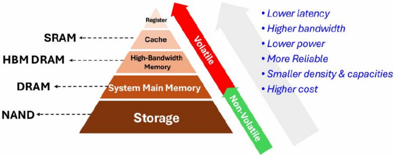
The Six-Layer Memory Cake: From SRAM to Cloud Storage
Storage / Memory Layer
On-Chip SRAM
L1 / L2 / L3 cache, register file, shared memory
- 3DStacked SRAM and Near-Field Wireless Interconnect: A New Memory Bottleneck Solution for AI Inference Chips
- 3DStacked SRAM Better Suited for Low-Latency AI Inference Than DRAM
CXL-attached memory expansion / pooled
- The Key Challenge Is Interconnect: TSV Is Not the Only Possible Answer memory
- From Multi-Drop to Multi-Hop: The Battle for Memory Bandwidth Density cluster
- Fujitsu MONAKA A 3DStacked SRAM CPU Architecture Built for the Next Era of AI and HPC
- Why MONAKA Moves Away from HBM
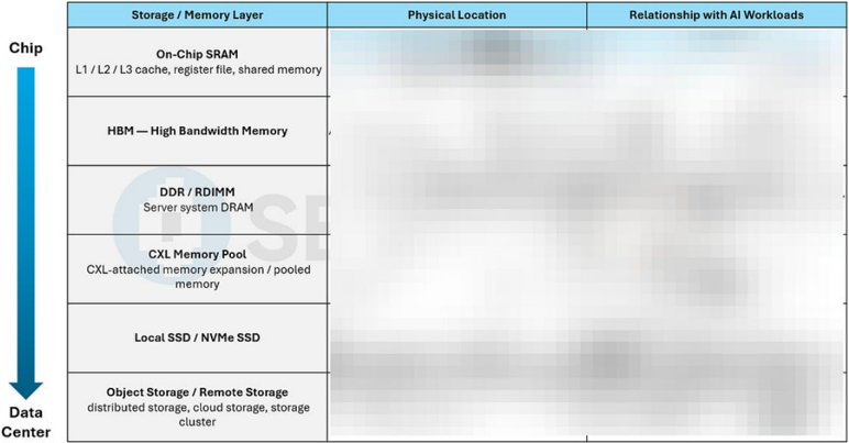
Physical Location
Relationship with Al Workloads
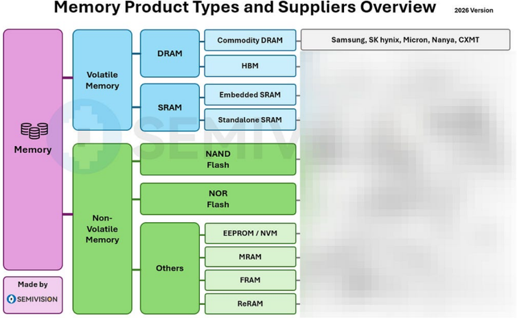
Memory
Made by
© SEMIVISION
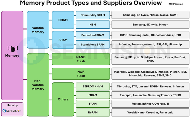
Memory Product Types and Suppliers Overview
Commodity DRAM
HBM
2026 Version
Samsung, SK hynix, Micron, Nanya, CXMT
Volatile
Memory
Non-
Volatile
Memory
3DStacked SRAM and Near-Field Wireless Interconnect: A New Memory Bottleneck Solution for AI Inference Chips
The competition in AI hardware is shifting from raw compute to data movement efficiency. In the past, discussions around AI chips often focused on MAC arrays, process nodes, TOPS, or GPU cluster scale. But in real AI inference workloads, the true system bottleneck is often not the compute unit itself, but how fast and how efficiently data can be delivered to that compute unit. This is why 3D-stacked SRAM is becoming increasingly important: as AI inference moves into edge devices, autonomous driving, factory automation, and real-time sensing, low-latency, low-power, high-bandwidth memory will become a central pillar of system architecture.
DRAM
Chip
Data
Center
The Six-Layer Memory Cake: From SRAM to Cloud Storage
Storage / Memory Layer
On-Chip SRAM
SRAM
Relationship with Al Workloads
Stores the hottest data, including instructions, operands, activations, partial sums, and
frequently reused data
Physical Location
Inside the CPU, GPU, or Al accelerator die, closest to compute units
3D-Stacked SRAM Using Near-Field Wireless Communication
L1 / L2 / L3 cache, register file, shared memory
HBM - High Bandwidth Memory
Inside the advanced package, next to the GPU / Stores model weights, activations, KV cache,
Al accelerator die, usually connected through an optimizer states, and high-throughput training /
Kota SHIBA’*, Atsutake KOSUGE’, Mototsugu HAMADA’,
DDR / RDIMM
Server system DRAM
’, and Tadahiro KURODA’
’ Dept. of EEIS, The University of Tokyo (The University of Tokyo 7-3-1 Hongo, Bunkyo-ku, Tokyo 113-8656)
CXL Memory Pool memory
CXL-attached memory expansion / pooled
Local SSD / NVMe SSD
Object Storage / Remote Storage cluster
distributed storage, cloud storage, storage
| interposer or advanced packaging structure inference data |
|---|
| Stores host-side runtime data, data On the server motherboard, connected to the preprocessing buffers, OS / application memory, CPU memory channels CPU-side tensors, and sometimes offloaded |
| Inside the server, chassis, or rack; attached through CXL memory expanders, switches, or pooled memory devices Provides memory expansion, pooled memory capacity, elastic sharing, and potential offload capacity for large Al workloads |
| Inside the server or rack; connected through PCle / NVMe Stores checkpoints, datasets, logs, indexes, containers, model files, and can support KV cache or model offloading when HBM / DRAM |
| Rack, data center, or cloud infrastructure level Stores training datasets, cold data, backups, archives, snapshots, model repositories, and long-term storage |
The Real Bottleneck in AI Inference Is Not Computation, but Memory Access
AI inference hardware performs massive amounts of matrix multiplyaccumulate operations. However, as AI models move toward low-bit quantization, the energy cost of computation itself has fallen sharply. The paper notes that an 8-bit addition consumes only about 0.03 pJ, while an 8-bit multiplication consumes about 0.2 pJ. By contrast, a 64 bit DRAM access requires around 1.3 to 2.6 nJ. In other words, as AI models move from FP32 to INT8, 4-bit, or even binary/ternary formats, the expensive part is no longer ‘computing’; it is ‘moving data.’
Memory
25*14
Memory
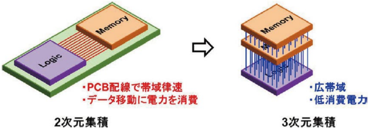
This has major implications for AI chip design. In conventional architectures, logic chips and memory chips are placed side by side, forcing data to travel over relatively long distances. By contrast, 3D stacking places the memory chip directly above the logic chip, reducing data movement distance from several centimeters to only tens or hundreds of micrometers. This is not just a packaging transition. It is a fundamental restructuring of the dataflow architecture.
3DStacked SRAM Better Suited for Low-Latency AI Inference Than DRAM
3D SRAM V-Cache
• SRAM area scaling increases barrier to have large on-die SRAM cache.
• 3D-stacked V-Cache improves LLC SRAM capacity, latency and bandwidth
3D-stacked memory is not a single technology path. HBM represents 3D-stacked DRAM, while this paper focuses on 3D-stacked SRAM. Although SRAM has higher cost per bit, it offers lower latency, random access capability, and no refresh requirement. The paper highlights that 3D-stacked SRAM can achieve memory access power roughly one order of magnitude lower than 3D-stacked DRAM, while also delivering roughly one order of magnitude lower latency. 1.36X Far Cry”& Gears 5™ Shadow of the… CS:GOTM
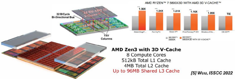
The AMD Ryzen™ 7 5800X3D processor uses this technology, integrating 8 computing cores, 512KB L1 cache, 4MB L2 cache, and a shared L3 cache of up to 96MB. Through a 32-byte/cycle bidirectional bus, it has achieved a leapfrog improvement in cache performance and significantly improved gaming performance, fully verifying the enabling effect of 3D stacked SRAM on computing performance.
This is particularly important for AI inference. Cloud-based AI training can tolerate higher latency in exchange for massive throughput. But edge inference, autonomous driving, robotics, and real-time industrial control require fast and deterministic response. This makes 3D SRAM not merely a ‘faster memory,’ but a potential architectural foundation for AI edge SoCs, inference accelerators, and large-cache processors.
SRAM *-
HBM DRAM
DRAM +—
NAND *
Register
Cache
The paper also cites several performance gains from prior research: 3D-stacked SRAM can improve AI accelerator performance by up to 2.1x, improve CPU performance by up to 1.25x when used as a largecapacity cache, and improve pruned DNN accelerator performance by up to 1.4x. This shows that the value of 3D SRAM is not limited to one type of AI accelerator. It may extend into CPU cache, sparse neural networks, and broader memory-centric computing architectures.
When HBM Becomes ‘Luxury Real Estate for Compute’ How to Rebuild AI Memory Architecture
SEMIVISION · MAY 18
Read full story
The Key Challenge Is Interconnect: TSV Is Not the Only Possible Answer
To make 3D-stacked memory viable, the critical question is how to connect the upper and lower chips. The traditional solution is wired interconnect using TSVs and micro-bumps. However, this approach requires additional process steps, creating challenges in cost, yield, and reliability. The core technology discussed in this paper is near-field wireless interconnect, known as ThruChip Interface, or TCI, as an alternative to some conventional wired interconnect structures.
• Lower latency
• Higher bandwidth
Logic
Wafer Process
Additional cost
TSVEn-bump
Receiver
Coil
стокового солот
TSV vs. TCI 7)
TSV
Additional steps
> 40%
TCI
Standard CMOS
A few %
FAIRSAM E
(a) TSVE-bump& L*=14/ SRAM
Transmitter coil
SOC
Logic
| Low Needed | |
|---|---|
| Needed | No need No need |
| Needed | No need |
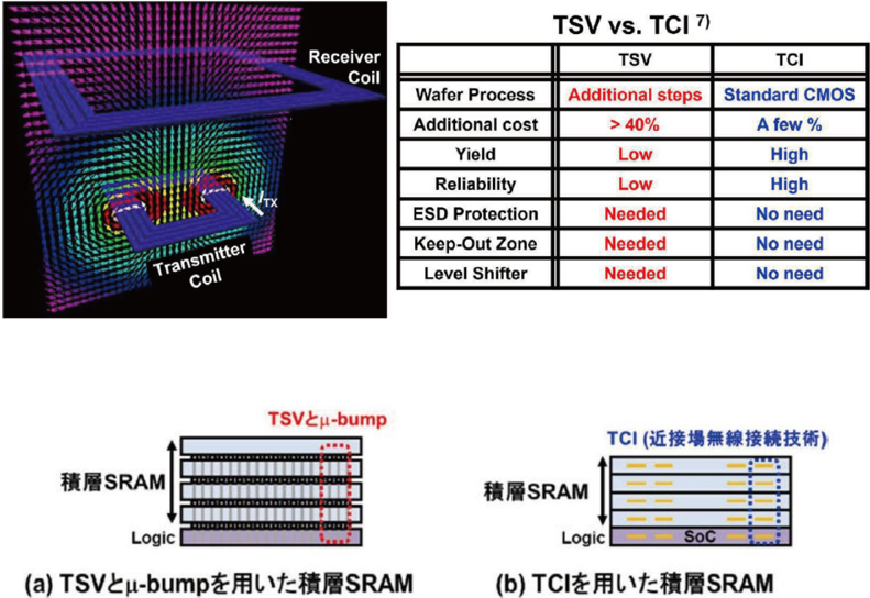
TCI uses on-chip coils to generate magnetic fields, allowing inductive communication through stacked chips. Since these coils can be fabricated using a standard CMOS process, TCI avoids the additional through-silicon via process required by TSVs. It can also eliminate the need for ESD protection circuits, keep-out zones, and level shifters. From a manufacturing perspective, this implies lower cost and potentially higher yield. From an architectural perspective, it suggests that 3D stacking does not necessarily have to rely entirely on expensive and complex vertical metal vias.
TSV vs. TCI
Method
Wafer Process
Package Process
Miniaturization
Yield
Eco-system
Additional Cost
Placement
Speed
ESD Protection
Power
Tadahiro Kuroda
TSV
transistor mcro bump
TCI
transistor
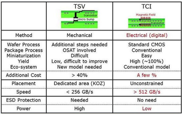
| Mechanical Additional steps needed OSAT involved Difficult | Electrical (digital) Standard CMOS Conventional Easy |
|---|---|
| Low, difficult to improve New model needed | High (~100%) Conventional model |
| > 40% Dedicated area (KOZ) < 256 GB/s Needed | A few % Unconstrained > 512 GB/s No need |
| High | |
| Low |
From a SemiVision perspective, the importance of this technology is not that it will immediately replace TSVs. Rather, it points to a broader direction: future advanced packaging and 3D integration will not follow a single path. Instead, multiple interconnect technologies will coexist, depending on power, bandwidth, cost, yield, reliability, and application requirements.
From Multi-Drop to Multi-Hop: The Battle for Memory Bandwidth Density
Early TCI-based stacked SRAM used multi-drop communication, where one transmitter sends data to multiple receivers at the same time. The advantage is that power consumption does not increase sharply as more memory layers are added. However, the drawback is that as the number of stacked layers increases, the coil size must also increase, reducing memory bandwidth per unit area. The paper notes that the area efficiency degrades quadratically with the number of stacked layers.
This is why research has shifted toward multi-hop communication. Instead of sending data to all SRAM chips at once, data is transferred layer by layer. This enables the use of ultra-small coils at the 10 micrometer scale, improving both area efficiency and memory bandwidth. The key point here is that the 3D-stacked memory is no longer treated as a simple vertical connection. It becomes a vertical communication network.
This echoes a broader trend in AI hardware. Future chips will not be defined only by single-die design, but by the topology among die-todie, chiplet-to-chiplet, and memory-to-logic connections. Whoever can deliver the highest effective bandwidth with the smallest area and lowest power will gain a structural advantage in AI inference architecture.
CH1
Downlink
CH2
Link Link Link Link
Link
Link Link
1-1
1-2 1-3
1-4
RX
RX
1X
CLK]
TX
- IX:Enabled
— TX:Sleep
P [um]
2-2
2-3
RX
Mem.
Mem.
Uplink
CH(n-1)
CHn
Link
Link Link Link
Link Link Link Link
(n-1)-1 (n-1)-2 (n-1)-3 (n-1)-4 n-1
n-2
n-3
n-4
TX
RX
#8
#7
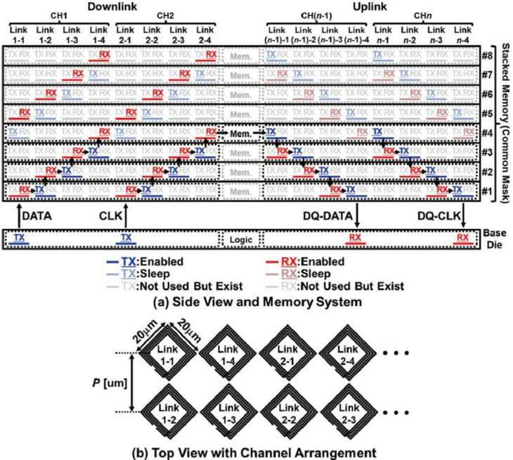
The New Challenge of High-Density Wireless Interconnect: Crosstalk
While multi-hop TCI improves area efficiency, it also introduces a new problem: crosstalk. When a large number of coils operate simultaneously, the magnetic field generated by one communication channel may interfere with neighboring channels, creating noise at the receiver. The paper describes the disturbed channel as the ‘victim’ and the interfering channel as the ‘aggressor.’
This problem is fundamental. To increase bandwidth in 3D-stacked memory, more communication channels must be packed into a limited area. But the denser the channels become, the more severe the
2-1
XRX TXR)
RX
XRI
RX
RX
TX
IXRX
RX→TX
RX+TX
DATA
TX
Link
2-4
RX
Stacked Memory (Common Mask)
vL
crosstalk becomes. This creates a three-way trade-off among bandwidth, area efficiency, and signal integrity.
This is the same type of system-level challenge seen in high-speed PCBs, SerDes, HBM packaging, and co-packaged optics. System performance is no longer determined only by device specifications. It is determined by electromagnetic behavior, packaging layout, signal integrity, and architecture-level co-optimization.
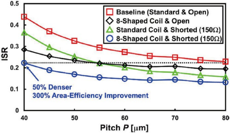
Shorted Coils and 8Shaped Coils: Suppressing Crosstalk Through Structural Design
The paper proposes two methods to reduce crosstalk. The first is the shorted coil. The concept is to use inactive transmitter coils and short them with low resistance. When magnetic fields pass through these shorted coils, eddy currents are generated, which attenuate the interfering magnetic field. The advantage is that this method does not require an additional metal plane, major floorplan changes, or extra process cost.
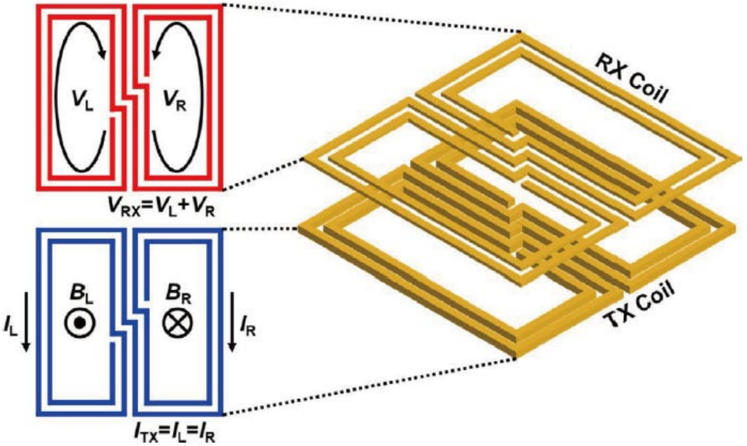
The second method is the 8-shaped coil. This coil is composed of two rectangular coils wound in opposite directions and uses differential magnetic fields for communication. Because common-mode interference from neighboring coils can be cancelled, the structure can effectively reduce crosstalk from laterally adjacent channels. The paper notes that 8-shaped coils had previously been used in full-duplex communication, but here they are applied to suppress magnetic-field interference from neighboring coils on the same chip.
Simulation results show that shorted coils mainly reduce crosstalk from concentrically arranged coils, while 8-shaped coils reduce crosstalk from laterally adjacent coils. When both methods are combined, the coil pitch can be reduced from 80 micrometers to 40 micrometers under the same ISR condition, resulting in a 4x improvement in area efficiency. This is one of the most important findings of the paper because it directly addresses the scalability of high-density 3D SRAM interconnect.
throughput computing. 3D SRAM is more likely to solve the low-latency, SemiVision View: 3D SRAM Is Not a Replacement for HBM, but a New Layer in the AI Memory Hierarchy
From an industry perspective, 3D-stacked SRAM should not be simplified as a replacement for HBM or DRAM. HBM solves the highcapacity, high-bandwidth memory problem for AI training and highlow-power, near-compute memory problem for AI inference.
Future AI memory architecture will become increasingly hierarchical. HBM will provide large external bandwidth, on-chip SRAM will provide high-speed local cache, and 3D-stacked SRAM may emerge as an intermediate layer that delivers high bandwidth, low latency, and closer physical proximity to the logic core.
More importantly, TCI is not merely an interconnect technique. It reflects the broader system integration logic of the post-Moore era. As transistor scaling slows, AI chip performance improvement will rely increasingly on packaging, interconnect, memory hierarchy, and
0.5
, 0.3 g
0.2
0.1
0
40
Baseline (Standard & Open)
• 8-Shaped Coil & Open dataflow design. The next stage of competition will not take place only at the process-node level. It will also take place in vertical stacking, low-power interconnect, electromagnetic design, and system-level cooptimization.
50% Denser
300% Area-Efficiency Improvement
Conclusion: The Next AI Chip War Is About Bringing Memory Closer to Compute
The real significance of this research is that it reveals the next direction of AI inference hardware: not simply adding more compute units, but moving data with lower power, lower latency, and higher density near the compute core. 3D-stacked SRAM provides this direction, while TCI near-field wireless interconnect offers a possible path to lower cost and higher yield.
The future of AI hardware will shift from ‘who has more compute’ to ‘who can move data more efficiently.’ Under this trend, 3D SRAM, nearfield wireless interconnect, chiplet architecture, advanced packaging, and memory hierarchy design will jointly become a core battlefield in the next phase of AI semiconductors.
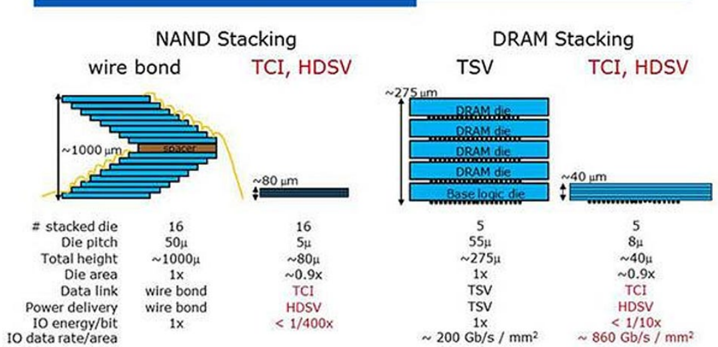
Memory Stacking with TCI and HDSV
NAND Stacking wire bond
TCI, HDSV
~1000 urr
stacked die
Die pitch
Total height
Die area
Data link
Power delivery
10 energy/bit
10 data rate/area
16
50u
~1000g
1x wire bond
wire bond
1x
~275 um.
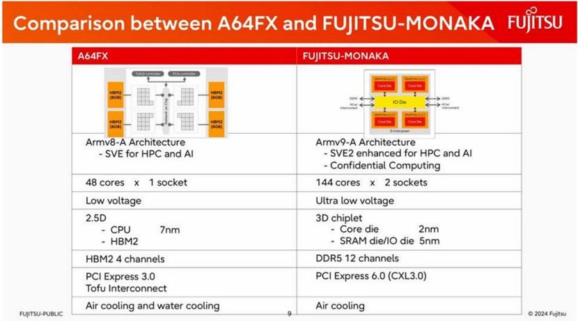
Fujitsu MONAKA A 3DStacked SRAM CPU Architecture Built for the Next Era of AI and HPC
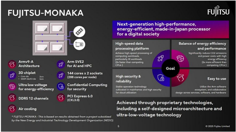
Fujitsu’s MONAKA processor represents a strategic shift in highperformance CPU design. Instead of relying purely on aggressive logic scaling or external high-bandwidth memory, MONAKA adopts a more system-level architecture: advanced Arm cores, 3D-stacked SRAM cache, chiplet-style integration, and a cost-aware split between leading-edge and mature process nodes.
DRAM Stacking
TSV
TCI, HDSV
FUJITSU

According to Fujitsu, MONAKA is designed to deliver a major leap in both energy efficiency and application performance. With technologies such as ultra-low-voltage processing, the company claims the CPU can achieve twice the energy efficiency of competing processors expected around 2027, while avoiding the need for water cooling. Fujitsu also states that MONAKA’s application-level performance could reach twice that of rival products.
At the instruction-set level, MONAKA upgrades its vector capability to SVE2, making the processor better suited for AI and HPC workloads. It also adds support for confidential computing, reflecting the growing importance of secure computation in cloud, enterprise, and sovereign AI infrastructure.
FUJITSU-MONAKA-X (1.4nm)
No.1 Processor made in Japan that leads the industry in the Al inference era
Low-latency inference
World’s first server CPU with Arm SME
Real-time
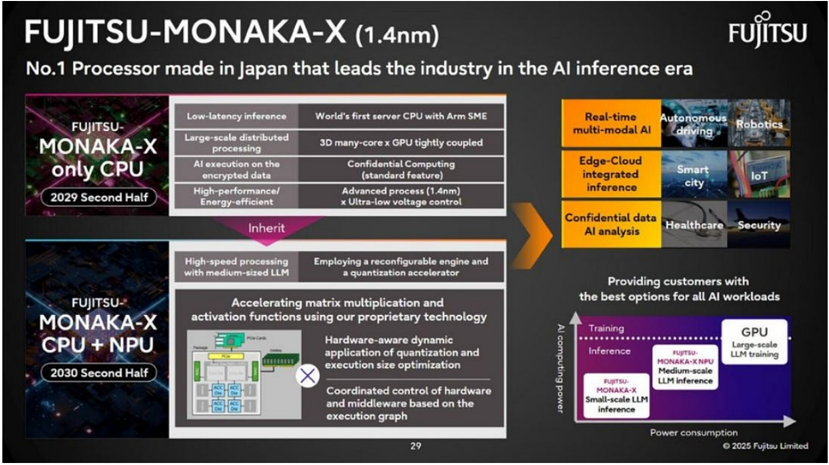
Autonomous
FUJITSU
Robotics
A 144Core Armv9 CPU with Dual-Socket Support
MONAKA supports dual-socket configurations, with each CPU integrating 144 Armv9 cores. This positions the processor as a serious candidate for next-generation AI infrastructure, HPC systems, and energy-efficient data centers where performance-per-watt is becoming as important as peak performance.
The architecture is not a conventional monolithic CPU. Each MONAKA processor consists of a central I/O die and four vertically stacked 3D complexes. These components are connected through a silicon interposer and package substrate underneath, forming a highly integrated chiplet-style system.
Each 3D complex combines a processor core die with an LLC SRAM die. The core die is placed above the SRAM die, allowing the CPU cores to access a large last-level cache with much higher bandwidth and lower latency than a conventional off-chip memory path.
FUJITSU-
MONAKA-X
only CPU
2029 Second Half
FUJITSU-
MONAKA-X
CPU + NPU
2030 Second Half
FUJITSU-MONAKA Targets and Roadmap
FUjITSU
Supporting Al Foundations globally with state-of-the-art computing made in Japan
Sovereign infrastructure target: Defense, government, healthcare, finance (part manufacturing (part)
Data Center
High-performance, low-power consumption FUjITSU-MONAKA platform to meet growing demand in data centers
Al services
2011
SPARC64
K
World-class performance
Massively Parallel SPARC
Supercomputer
Lower TCO
2020
45.m

A64FX
Fugaku
2nm Logic, 5nm SRAM and I/O A Cost-Aware Process Strategy
One of MONAKA’s most important design choices is its heterogeneous process strategy. The core die is manufactured using a 2nm process, while the underlying SRAM die and the central I/O die use a more mature 5nm process.
This is not only a technical decision, but also a cost-control strategy. Fujitsu says the 2nm portion accounts for only around 30% of the total die area. In other words, the most expensive leading-edge process is used only where it delivers the highest value: the compute cores. SRAM and I/O, which do not necessarily benefit from 2nm scaling in the same way, are implemented on a more mature node.
This reflects a broader trend in advanced semiconductor design. Future high-performance processors will increasingly avoid placing every function on the most advanced node. Instead, logic, cache, I/O, analog, and memory components will be disaggregated and manufactured on the most suitable process node, then recombined through advanced packaging.
Security
FUJITSU-MONAKA
Armv9-А
Architecture
3D chiplet
2nm
• Core die
• SRAM die/O die
5nm
Ultra low voltage for energy-efficiency
DDR5 12 channels
Air cooling
- FUJITSU-MONAKA: This is based on results obtained from a project subsidized by the New Energy and Industrial Technology Development Organization (NEDO).
Next-generation high-performance, for a digital society
FUjITSU
energy-efficient, made-in-japan processor
MONAKA adopts 2nm process technology and uses hybrid copper bonding (HCB) to stack the compute die face-toface (F2F) on top of SRAM modules manufactured using 5nm process technology. Fujitsu will integrate the compute modules, SRAM modules, and I/O modules together. The I/O module also incorporates memory controllers and provides connectivity channels supporting the CXL 3.0 and PCIe 6.0 standards.
Why MONAKA Moves Away from HBM
Another notable architectural decision is MONAKA’s move away from HBM. Fujitsu’s previous A64FX processor, used in the Fugaku supercomputer, adopted HBM to deliver high memory bandwidth. MONAKA, however, uses 12-channel DDR5 memory instead.
This may seem counterintuitive at first, especially in an AI and HPC market increasingly dominated by HBM. But the logic becomes clearer when considering MONAKA’s 3D-stacked SRAM architecture. Because the on-package 3D SRAM cache already provides high internal bandwidth close to the compute cores, Fujitsu can reduce its dependence on expensive off-package HBM.
Comparison between A64FX and FUJITSU-MONAKA FUjITSU
A64FX
HBM?
(8G8)
HBM2
(808)
2.5D
FUJITSU-MONAKA
This does not mean HBM is becoming less important across the industry. Rather, it shows that memory architecture is becoming more workload-specific. For GPU training systems and large AI accelerators, HBM remains essential. For CPU-centric AI, HPC, and cloud workloads, a large, high-bandwidth 3D SRAM cache combined with DDR5 may offer a better balance of cost, power, capacity, and system scalability.
HBM2 4 channels
DDR5 12 channels
PCI Express 3.0 Tofu Interconnect Air cooling and water cooling PCI Express 6.0 (CXL3.0) Air cooling
PCIe 6.0 and CXL 3.0 Built for Disaggregated Infrastructure
MONAKA also supports PCIe 6.0 and CXL 3.0, indicating that Fujitsu is designing the processor not only as a standalone CPU, but as part of a broader disaggregated computing infrastructure.
PCIe 6.0 provides higher-speed connectivity for accelerators, networking, storage, and other peripheral devices. CXL 3.0, meanwhile, enables more flexible memory expansion, memory pooling, and coherent interconnect between CPUs, accelerators, and memory devices.
This is highly relevant for the next phase of AI and HPC infrastructure. As systems scale beyond a single server, performance increasingly
FUJITSU-PUBLIC
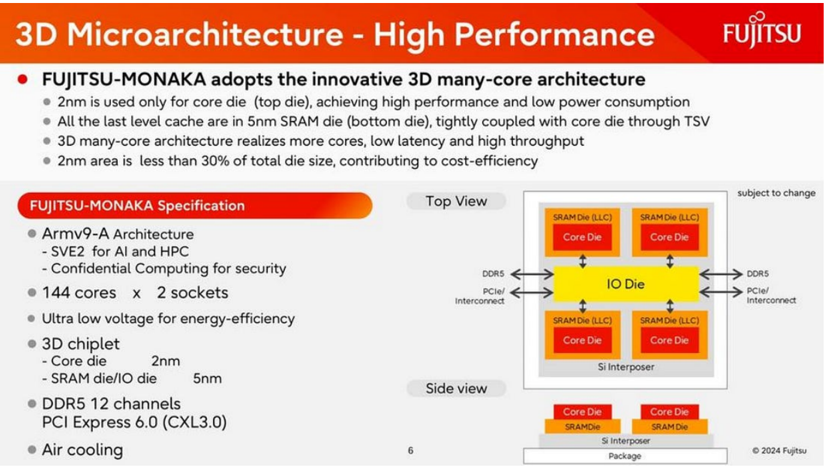
3D Microarchitecture - High Performance
• FUJITSU-MONAKA adopts the innovative 3D many-core architecture
• 2nm is used only for core die (top die), achieving high performance and low power consumption
• All the last level cache are in 5nm SRAM die (bottom die), tightly coupled with core die through TSV
depends on how efficiently compute, memory, accelerators, and networking resources can be composed. MONAKA’s support for CXL 3.0 suggests that Fujitsu is preparing for a data center architecture where memory and compute are less tightly bound to a single motherboard and more dynamically allocated across the system.
• Ultra low voltage for energy-efficiency
• 3D chiplet
-
Core die
-
SRAM die/1O die
• Air cooling
SRAM Die (LLC)
Core Die
SRAM Die (LLC)
Core Die
SemiVision View: MONAKA Shows the Future of CPU Design Is Packaging-Driven Side view
Core Die
Core Die
From a SemiVision perspective, MONAKA is important because it shows how advanced CPU design is becoming packaging-driven rather than purely node-driven. The processor combines Armv9 cores, SVE2 vector instructions, 3D-stacked SRAM, silicon interposer integration, PCIe 6.0, CXL 3.0, and heterogeneous process nodes into one system-level architecture.
The key message is clear: the future of AI and HPC processors will not be decided only by who uses the most advanced logic node. It will be decided by who can allocate the right function to the right process, place memory closer to compute, reduce data movement energy, and build a scalable package-level architecture.
FUjITSU
MONAKA’s 3D-stacked SRAM is especially significant. It points to a new memory hierarchy where high-bandwidth, low-latency cache becomes a central design element. This is different from the GPU/HBM model, but it may be highly effective for CPU-centric AI inference, HPC, cloud-native workloads, and energy-constrained data centers.
Conclusion: MONAKA Is a Signal of the Post-Moore CPU Era
Fujitsu MONAKA is more than a new server CPU. It is a signal of where high-performance processor architecture is heading in the post-Moore era. The industry is moving from monolithic scaling to heterogeneous integration. It is moving from external memory bandwidth dependence to near-compute memory design. It is moving from peak performance marketing to performance-per-watt, cooling efficiency, and systemlevel cost optimization. performance gains will come not only from smaller transistors, but from
If MONAKA delivers on Fujitsu’s claims, it could become an important reference architecture for the next generation of AI and HPC CPUs. More importantly, it reinforces a broader industry direction: future smarter integration of compute, cache, memory, interconnect, and packaging.
Memory
Made by
O SEMIVISION
Memory Product Types and Suppliers Overview
Commodity DRAM
HBM
2026 Version
Samsung, SK hynix, Micron, Nanya, CXMT
Samsung, SK hynix, Micron
Thanks for reading SEMIVISION @_! This post is public so feel free to share it.
Volatile
Memory
Non-
Volatile
Memory
DRAM