PDF 原檔:EMIB-T HBM4 Challenges Microfluidic Cooling Photonic Interconnects_original.pdf
原始內容
EMIB-T, HBM4 Challenges, Microfluidic Cooling, Photonic Interconnects
newsletter.semianalysis.com /p/ectc2026
Afzal Ahmad, DC, Gerald Wong, Dylan Patel
July 2, 2026
As transistor density scaling has slowed, advanced packaging has become the primary scaling vector. However, AI accelerators have grown so large and require such fast interconnects that the package itself is now hitting limits. Circular interposers constrain package size and wafer utilization, HBM4E doubles the I/O count while increasing speed, and multi-kilowatt packages are overwhelming conventional cooling architectures.
ECTC is the industry's premier conference for all things packaging. This year's disclosures were closely aligned with upcoming commercial products. Intel provided an overview of EMIB-T integration, package scaling and future roadmaps. Marvell showed how custom HBM can move interface logic off the accelerator while shortening package routing. TSMC and Microsoft pushed coolant directly into silicon, while Marvell and Lightmatter brought optical interconnects onto the package.
This roundup covers ECTC 2026 technologies most likely to shape AI accelerator packages over the next several years.
Intel EMIB-T
Intel was the largest corporate presenter at ECTC. The key disclosure was EMIB-T. This is the next generation of EMIB with through-silicon vias (TSVs). After the initial announcement, Intel has filled in more of the architecture and roadmap, including tighter bump pitch, larger packages and on-bridge capabilities. Their disclosures show why EMIBT is expected to be used in Google's TPU v9, and why it is the most credible alternative to TSMC's CoWoS platform for large-package AI accelerators.
EMIB-T scaling test vehicle with 2× reticle silicon content. Top-down SEM images show 110, 55 and 36 µm mixed bump pitches. Source: Intel, 'Scaling the EMIB-T Advanced Packaging Technology to Address the Future HPC/AI Demand,' ECTC 2026
EMIB-T scaling test vehicle with 2× reticle silicon content. Top-down SEM images show 110, 55 and 36 µm mixed bump pitches. Source: Intel, 'Scaling the EMIB-T Advanced Packaging Technology to Address the Future HPC/AI Demand,' ECTC 2026
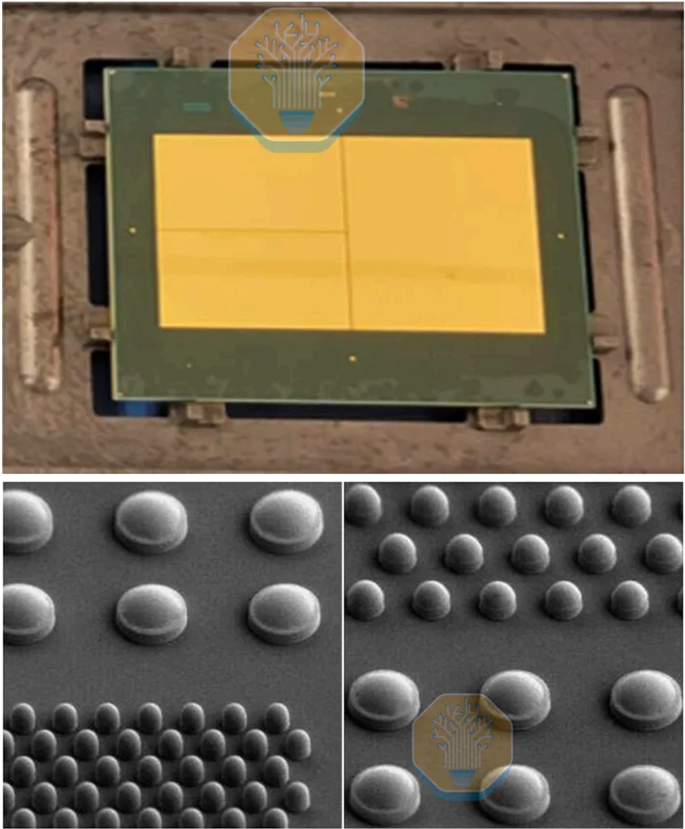
Intel has validated EMIB-T at a 36/35 µm bump pitch on a package with 2× reticle-sized silicon. This is a reduction over the 45 µm pitch used in Granite Rapids, and a 65% increase in bump density. Granite Rapids-AP is a large package, measuring 70 mm × 105 mm, or slightly less than 9 reticles of area. Validation for 36/35 µm bump pitches is now expanding to 4.5× reticle silicon packages, with certification targeted by the end of 2026.
240mm
240mm
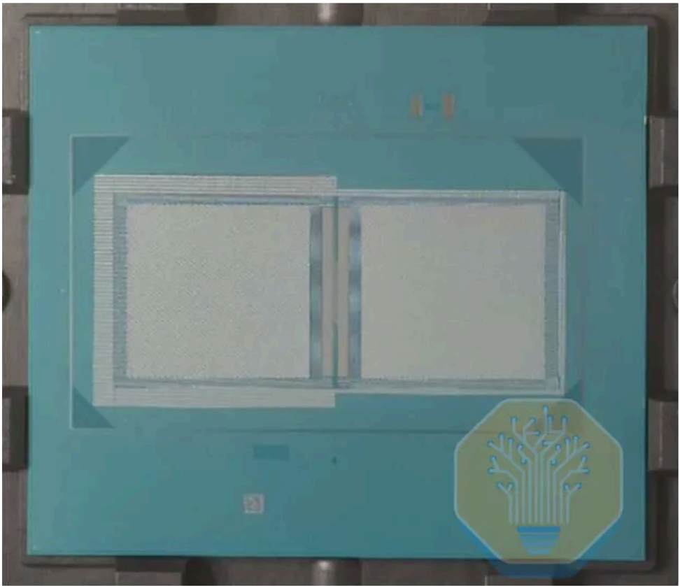
EMIB-T 25 µm bump pitch test vehicle with two 1-reticle silicon dies connected by a 3 mm × 18 mm bridge. SEM cross-section shows the post-assembly bump and via structure. Source: Intel, 'Scaling the EMIB-T Advanced Packaging Technology to Address the Future HPC/AI Demand,' ECTC 2026
The next pitch step is also underway, with Intel testing 25 µm bump pitch on a vehicle with two 1-reticle silicon dies connected through a single 3 mm × 18 mm EMIB-T bridge.
Further scaling gets harder. Below 25 µm, the solder volume in each bump becomes very small. Shorts, opens, and assembly-driven yield loss become much more likely. EMIB-T can keep scaling, but the limiter shifts from bridge routing density to bump formation, placement accuracy, and assembly yield.
Intel's 240 mm × 240 mm quarter-panel EMIB-T test vehicle. Source: Intel, 'Scaling the EMIB-T Advanced Packaging Technology to Address the Future HPC/AI Demand,' ECTC 2026
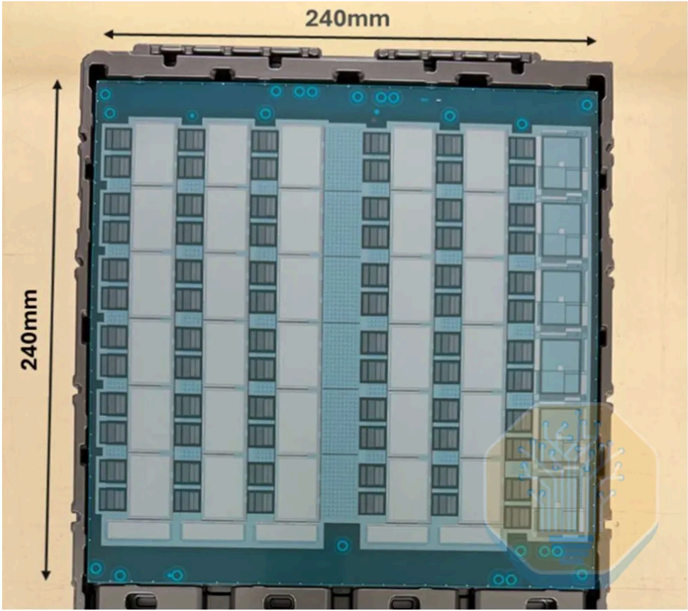
Intel also showed how large EMIB-T packages can become. Full panel-sized packages are possible, but Intel framed quarter-panel packages as the practical target. It showed a 240 mm × 240 mm test vehicle, equivalent to roughly 67 reticles of area. However, we observed that the sample at the booth exhibited severe warpage. At that size, the bridge is
M1O
M9
M8
M7
M6
M5
M4
M3
M2
M1
TSV
CSB
only one part of the problem. Substrate handling, warpage, overlay, and panel-level patterning become first-order constraints. Intel is also evaluating advanced lithography approaches to keep overlay tight enough for these large substrates at quarter-panel and even full-panel scale. traces with stitching via
EMIB-T stack-up with routing, power mesh, TSVs, and MIM layers. Source: Intel, 'Enabling 12+Gb/s HBM4E with EMIB-T Advanced Packaging Technology,' ECTC 2026
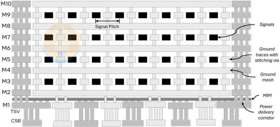
While bump pitch and package size are important, the bridges matter just as much. EMIBT is much more complex than the EMIB used in current products. It adds TSVs, more metal layers, a power mesh, and MIM capacitor layers so the bridge can carry both highdensity signals and vertical power delivery. Intel showed a cross-section with 10 metal layers, including 4 routing layers, and MIM capacitors between M1 and M2. Intel focused on its improvements for HBM4E.
Package DC Voltage Drop Comparison
DEMIB Package
4
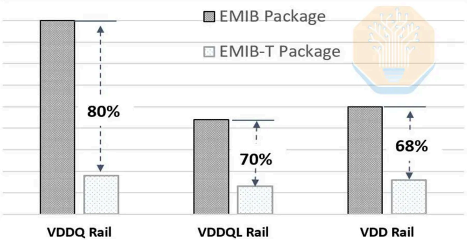
Package DC voltage drop using conventional EMIB vs EMIB-T. Source: Intel, 'Enabling 12+Gb/s HBM4E with EMIB-T Advanced Packaging Technology,' ECTC 2026
The 'T' in EMIB-T is for TSV. Their job is power delivery. In conventional EMIB, power is delivered vertically through the substrate in non-bridge regions, but power delivery near the bridges must spread laterally through the package and die-side routing. With TSVs in the bridge, power can be delivered directly through the bridge, reducing the current path distance significantly. Intel claims that DC voltage drop can be reduced by 68-80% with these TSVs.
HBM4E is difficult because the interconnect must scale both signal density and power delivery at the same time. HBM4 doubles the pin count versus HBM3, and the PHY needs additional power rails such as VDDQ and VDDQL. These rails take routing area away from signals, raising signal density in the remaining space.
To combat this, Intel did not route every HBM channel the same way. It placed the longest signal paths on cleaner routing layers. On M9, only ~28% of the longest channel length runs through the tightest routing region, while on lower layers such as M3, that number rises to ~84%, but those channels are shorter. This keeps crosstalk and insertion loss from being dominated by the worst routes.
Voltage
0.5
0.4
0.3
0.2
0.1
-0.1
-1
EMIB PDN Impedance (mOhm)
-5
0.5
0.4
EMIB-T package PDN AC impedance for HBM4E with and without bridge MIM capacitors. Source: Intel, 'Enabling 12+Gb/s HBM4E with EMIB-T Advanced Packaging Technology,' ECTC 2026
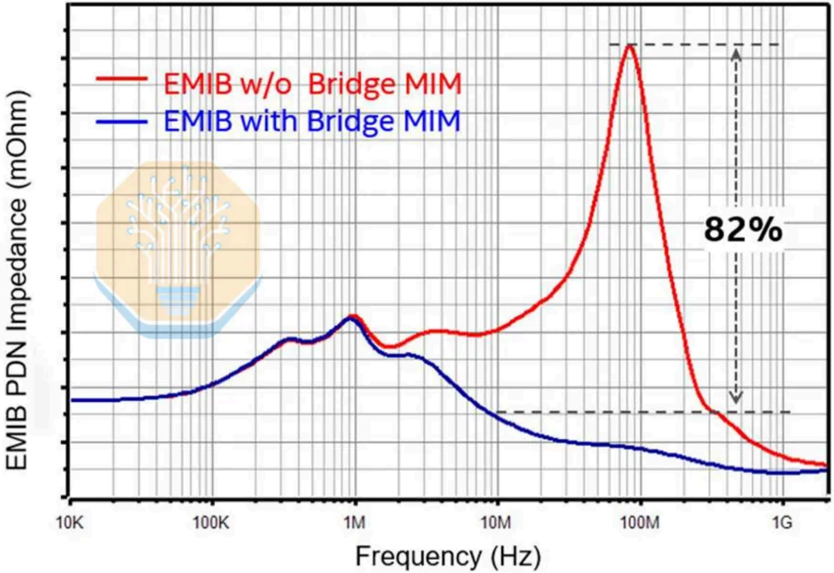
Power delivery is also moving into the bridge. EMIB-M introduced metal-insulator-metal (MIM) capacitors between M1 and M2, and EMIB-T builds on that approach. Intel disclosed a capacitance density of 500 nF/mm², roughly comparable to Intel 18A MIMs. Intel claims these on-bridge capacitors improve power delivery network (PDN) AC impedance by more than 82% versus an EMIB-T package without bridge MIM capacitors.
Signaling performance of HBM4E EMIB-T channel at 12 Gb/s without and with DFE. Source: Intel, 'Enabling 12+Gb/s HBM4E with EMIB-T Advanced Packaging Technology,' ECTC 2026
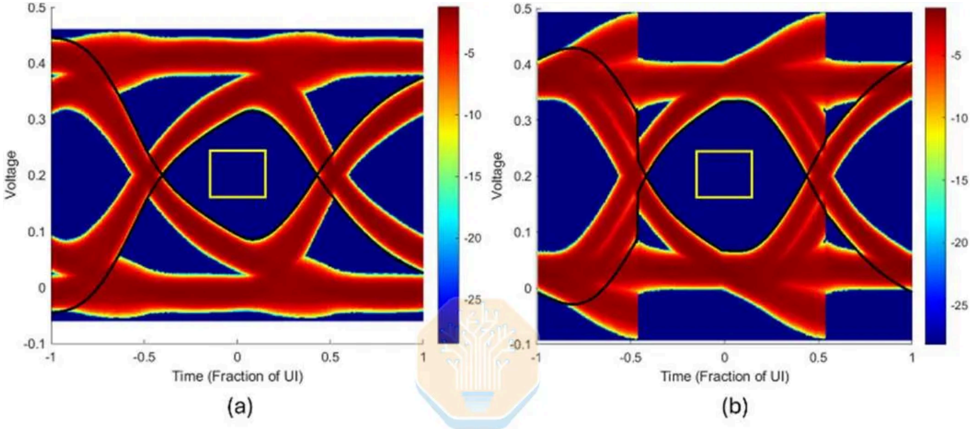
Intel also simulated EMIB-T with HBM4E. At 12 Gb/s, Intel showed ~67% UI eye width without receiver equalization. With a one-tap decision feedback equalizer (DFE), that improves to ~72.5%. A DFE is a receiver-side circuit that reduces interference from prior bits after the signal passes through the package channel.
Intel also simulated higher speeds of 12.8 Gb/s, 14 Gb/s and 16 Gb/s. The UI eye width remained above 60% at all tested speeds, with modest pad capacitance reduction.
Intel's EMIB roadmap goes beyond passive bridges with only routing and capacitors. Future versions include higher-density on-bridge MIM capacitors, larger high-aspect-ratio bridge dies, sub-25 µm bump pitch, active bridges, and embedded voltage regulators inside EMIB dies. Intel has also disclosed substrate-core embedded deep-trench capacitor (DTC) concepts and >2500 nF/mm² eMIM-T capacitors embedded below the base die, although we have not seen either in shipping EMIB products.
EMIB-T is still behind TSMC's CoWoS platform on several vectors. TSMC has already deployed DTC/eDTC integration and is further along on integrated voltage regulators and active local silicon interconnect (LSI). EMIB-T narrows the gap, but Intel is still catching up to an ecosystem that has been executing in volume for years.
Enhancing XPUs with custom HBM architecture
Marvell Custom HBM
Standard HBM
© 2034 Marvell. Al rights reserved.
Key content
• RAS and telemetry
• QoS
© 2025 Marvell All rights reserved
Marvell Custom HBM Summary and Base Die Floorplan. Source: Marvell, Industry Analyst Day 2024 and Hot Chips 2025
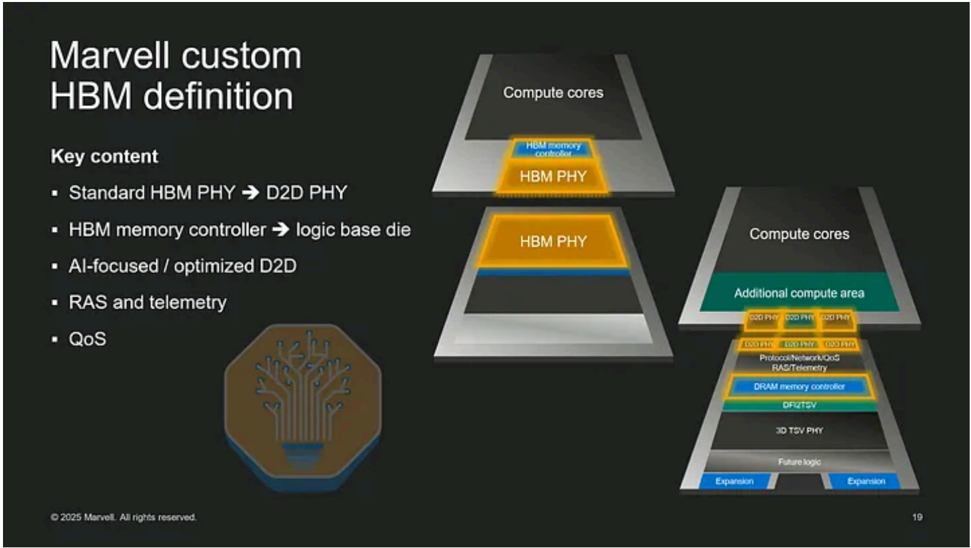
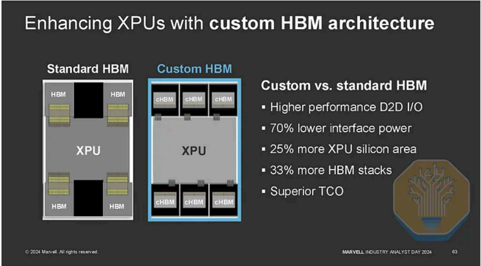
At Marvell's 2024 Industry Analyst Day, Marvell announced custom HBM. At the time, it was a vague claim with few technical details. HBM had been built around JEDEC compatibility: standard DRAM stacks from the memory vendors, standard HBM PHYs on the accelerator, and a fixed wide interface between them. At Hot Chips 2025, Marvell showed the floorplan of the custom base die. At ECTC, it finally provided the package-level details for custom HBM4E.
Custom HBM
Marvell cHBM → boundary shift
IEEE
ELECTRONICS
SOCIETY
ECTC
The 2026 ICE 76th Electronic Compel and technolesy Chaturence
The JEDEC specification fixes the interface between the HBM stack and host. That is good for interoperability: any memory vendor's HBM can be paired with any compliant host. However, it is bad for power, performance and area. The host ASIC must implement the standard HBM PHY and route a very wide, parallel interface with standardized pad placement and breakout rules. As packages get larger and HBM speeds rise, that fixed boundary makes it harder to optimize shoreline, routing density, power delivery and signal integrity. Standard HBM Custom HBM
CHBM
NOCRouing
3D TSV Phy:
· Reduced PHY/controller area on ASIC · More silicon area for core function / computation
IT MARVELL
ASIC
- Expansion Interfaces
Custom Logic
HBM Controller
NOC + Custom Bridge
- 2026 IEEE 76th Electronic Components and Technology Conference | Orlando, Florida | May 26 - May 29, 2026
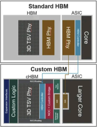
Standard HBM vs Custom HBM base die and host floorplan. Source: Marvell, 'Marvell custom HBM routing and signal integrity analysis,' ECTC 2026
Custom HBM keeps the DRAM core dies unchanged. Instead, a custom base die, with an optimized die-to-die interface, is fabricated on an advanced logic process. The custom base die can integrate the HBM controller, management and monitoring capabilities, custom logic, and expansion interfaces.
ErS PACKAGING
Routing Architecture
• Beachfront depth is the lever
• Beachfront depth governs breakout
- complexity + wires/mm + routing
efficiency
- CHBM reduces beachfront depth by ~67% · Shallower beachfront → less congestion
Parameters
Beachfront Depth
Beachfront Width
- and more efficient escape Routing Layers
- Vs deeper beachfronts correlate to higher insertion loss (longer routing) Line Width/Spacing (um)
- 911?
E| MARVELL:
Data Rate (Gbps)
Bandwidth (Tbps)
2026 IEEE 76*h Electronic Components and Technology Conference | Orlando, Florida | May 26 - May 29, 2026
JEDEC HBM4E vs Marvell Custom HBM. Source: Marvell, 'Marvell custom HBM routing and signal integrity analysis,' ECTC 2026
Marvell claims this reduces the host ASIC footprint dedicated to HBM PHYs and associated logic by ~60%, directly freeing up area for more compute, cache or I/O. The custom interface moves much of the memory-side interface into the HBM base die.
Marvell's example uses 1024 channels at 32 Gb/s, reaching 4.1 TB/s, equivalent to a 2048-bit JEDEC HBM4(E) interface at 16 Gb/s.
The package also gets easier to route, with the custom interface shortening the interposer channel length from 6.5 mm to 1.5 mm, allowing Marvell to keep the same 9 routing layers and 2/2 µm line/space (L/S) while increasing bandwidth.
Marvell's example uses an organic redistribution layer (RDL) interposer instead of silicon, reducing packaging costs. Organic RDL is limited to much coarser L/S than the silicon interposers in CoWoS-S or the silicon bridges in CoWoS-L and EMIB-T, which makes layout harder. Marvell relies on customized shielding and routing patterns in different sections to maximize bandwidth density while controlling crosstalk.
IEEE
IS PACKAGING®
ELECTRONICS
ECTC
SOCIETY
The 2026 KEE 16th Electronis Componen and technology Canturence
JEDEC
HBM4E
CHBM
| REF | REF / 3 |
|---|---|
| REF | REF |
| 9 | 9 |
| 2/2 | 2/2 |
| 12.8 | 64* |
| 26.2 | 32.8 |
| *Simultaneous bidirectional operation |
6
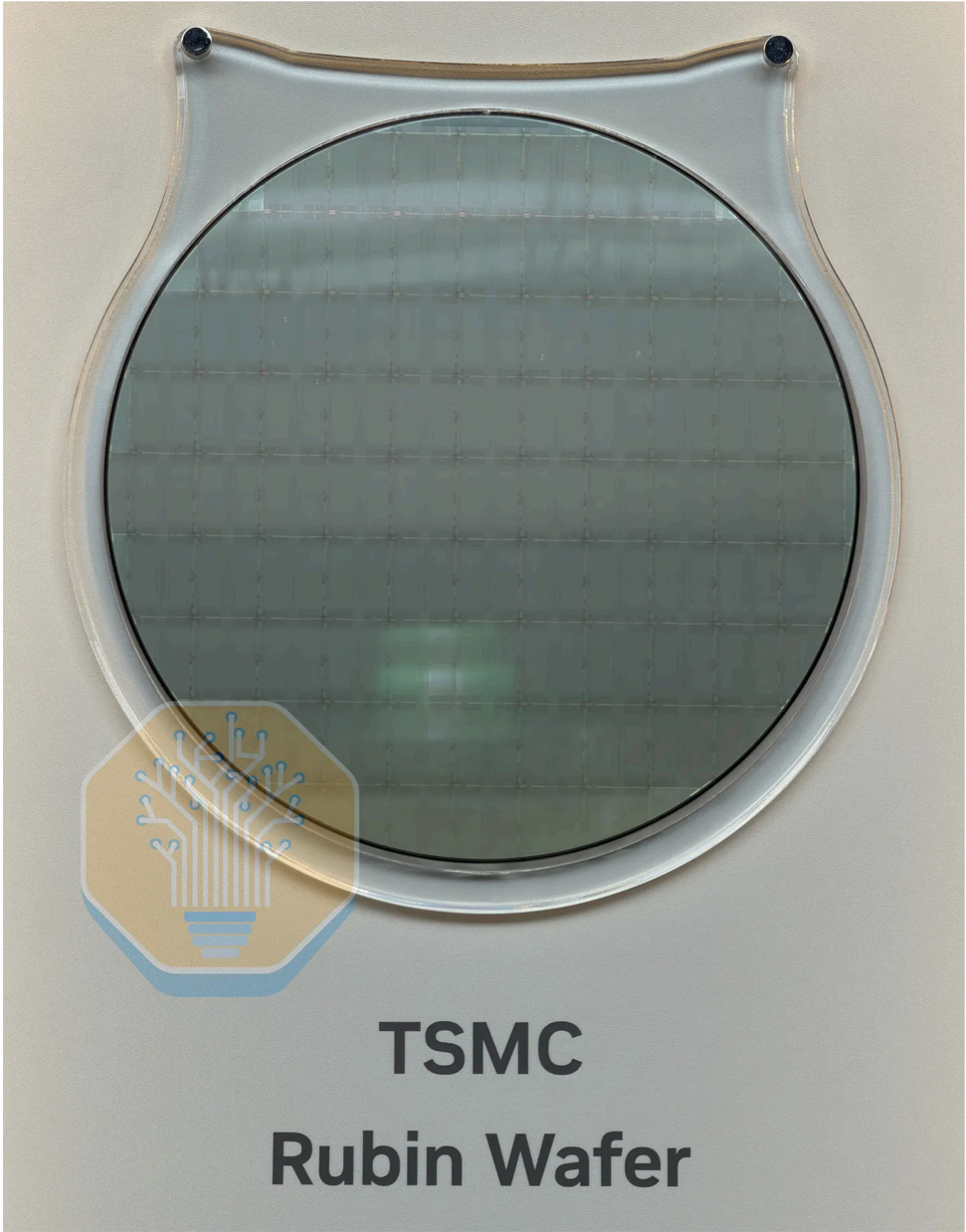
Nvidia Rubin GPU wafer. Source: TSMC, Computex 2026. Photo: SemiAnalysis
At GTC, Nvidia announced that Feynman would use custom HBM. Nvidia's reasons are likely similar to Marvell: higher bandwidth, lower power, and less accelerator die area dedicated to HBM. We estimate that ~16% of Rubin GPU die area is dedicated to HBMrelated logic and PHYs. Custom HBM allows Nvidia to offload much of that burden onto the HBM base die.
Custom HBM also enables expansion interfaces beyond the standard HBM link. Instead of forcing all memory traffic through the limited accelerator die shoreline, the base die can act as a secondary memory controller and fan out to additional memory. That memory could be higher-capacity, lower-bandwidth LPDDR, or even a second layer of HBM. This gives the accelerator a path to add capacity without consuming the valuable die shoreline needed for external I/O. This is relevant to AMD's upcoming MI450 and future MI500 GPUs, which will support LPDDR for increased memory capacity.
number of interposer layer x5
Power (a.u.)
6.0
5.0
4.0
2.0
1.0
0.0
5.6
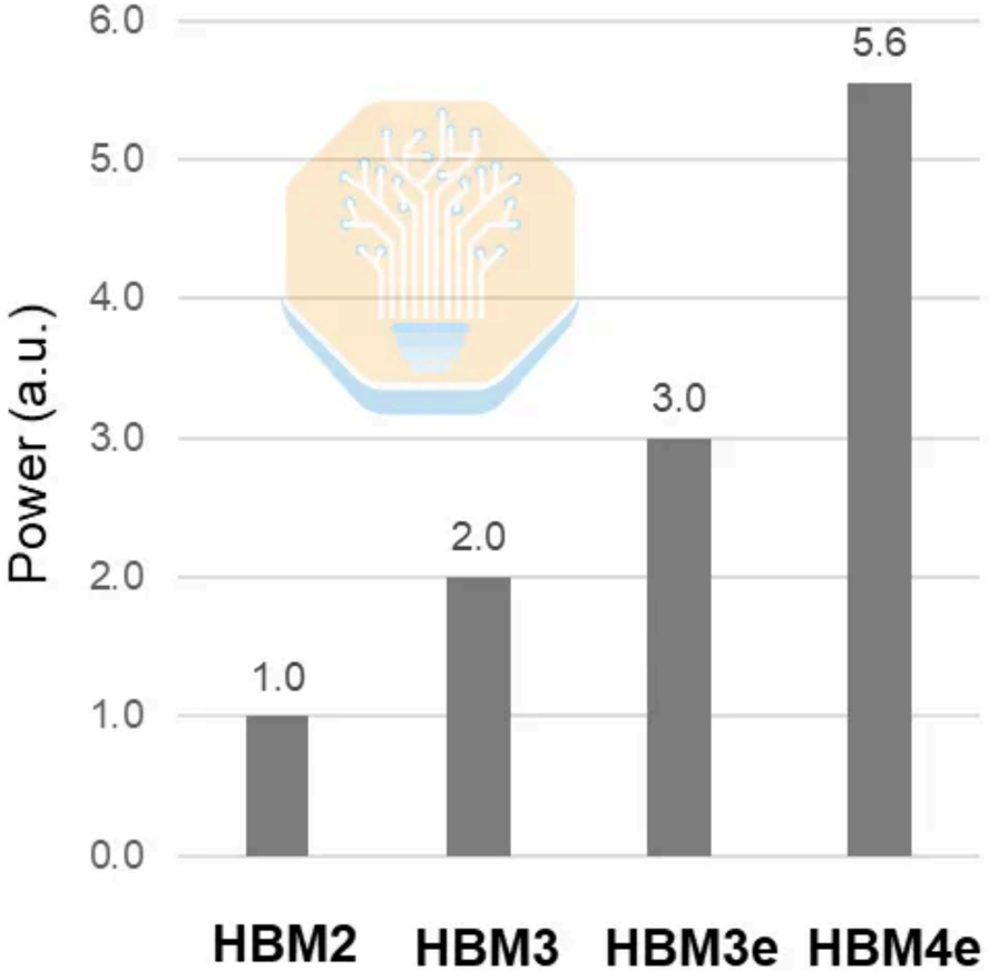
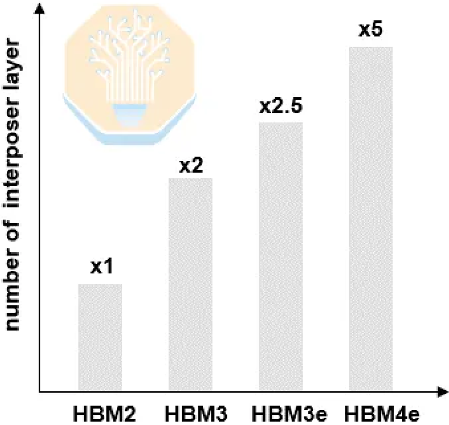
Interposer and power scaling from HBM2 to HBM4E. Source: Samsung, 'Advanced SI/PI Interposer Design Solution Enabling High-Performance HBM4e at up to 12Gbps,' ECTC 2026
Samsung also presented its solution for HBM4E on interposers. HBM4E pushes data rates to 12 Gb/s and above, and doubles the number of I/O pins, increasing routing complexity. HBM4E could require 2× the interposer layers versus HBM3E and 5× as much as HBM2. Due to the increased I/O count and higher data rates, power consumption is also expected to increase by 86% versus HBM3E, and 5.6 times versus HBM2.
M8
M7
M6
M5
M4
M3
M2
M1
8-layer silicon interposer stack-up for HBM4E with two-signal / one-ground routing. Source: Samsung, 'Advanced SI/PI Interposer Design Solution Enabling High-Performance HBM4e at up to 12Gbps,' ECTC 2026
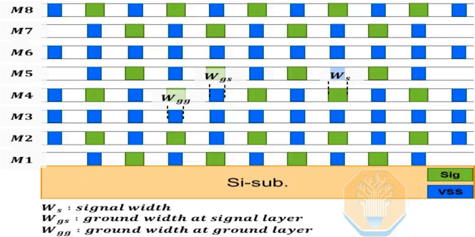
Samsung proposed an 8-layer silicon interposer which it says reduces the layer count by 20% versus the estimated requirement. The interposer stack uses a repeated two-signal / one-ground staggered arrangement to shield high-speed signals, with 75% of the layers being allocated for signal routing.
Another key aspect of the interposer is the ultra-high-density capacitors (UHCs). Samsung does not spell out the exact capacitor structure, but they are likely similar to Intel EMIB-T MIM capacitors or TSMC CoWoS DTCs. The UHCs can only be placed on the M1 layer, which is also heavily used for signal routing. Thus, the available area is limited.
M8
M7
M6
M5
M4
M3
M2
M1
CHO
Logic
HBM
M8
M7
M6
M5
M4
M3
M2
M1
CHO
Logic
HBM
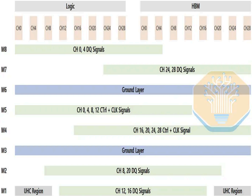
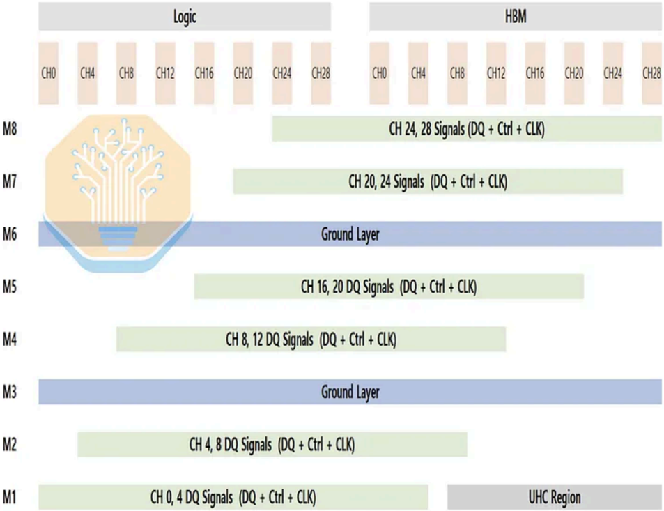
Unbalanced versus balanced capacitor layout in 8-layer silicon interposer. Source: Samsung, 'Advanced SI/PI Interposer Design Solution Enabling High-Performance HBM4e at up to 12Gbps,' ECTC 2026
If routing is unbalanced, the capacitors get pushed to one side of the interface, creating uneven PDN behavior between the logic and HBM sides. Samsung's layout redistributes the routing across M1 and the other layers so that UHCs can be placed more evenly across the entire interface. This reduces PDN impedance and voltage noise while keeping routing density manageable.
Package Thermal Design
Samsung HBM Hybrid Bonding Thermals
• HBM is becoming the thermal bottleneck due to increasing stack and power
Thermal Resistance Contribution in 2.5D
100%
75%
50%
Thermal Resistance Stackup (%)
IEEE
ELECTRONICS
SOCIETY
ECTC
The 2026 IELE 16th Electronic Campont
ETS PACKAGING
and lechnolngy Cenference
- 56 Cooling System 17 12 14 · Internal Crosstalk TIM1+Lid 40 35 Acceptable Range - 24-Stack HBM
SAMSUNG
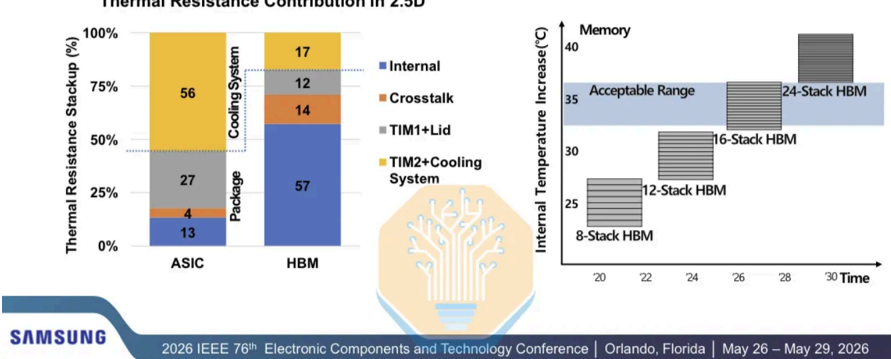
2.5D package thermal resistance contribution. Source: Samsung, 'System-Level Thermal Validation of 2.5D Packages in GPU Servers: Impact of TCB vs HCB HBM Platforms,' ECTC 2026
Samsung also discussed HBM thermals, particularly with hybrid bonding. HBM stacks are getting faster and taller, while the logic die underneath is also consuming more power. With 16-hi HBM, the thermal resistance is still acceptable, but with future generations moving to 20-hi and 24-hi HBM, new approaches are needed.
Internal Temperature Increase(°C)
Memory
(Air-TCB R_total =1.0)
Relative Thermal Resistance
1.200
1.000
0.800
0.600
0.400
0.200
0.000
SAMSUNG
IEEE
System Level HBM Thermal Resistance
ELECTRONICS
SOCIETY
ECTC
The 2026 HEL 76th Electronic Can
=ГS PACKAGING
and Technology Conference'
• Overall HBM system level thermal resistance: 7.6% reduction via HCB
-
Internal thermal resistance: 12.5% decrease
-
GPU-to-HBM thermal crosstalk: 9.8% reduction
- System Level HBM Resistance
System Level HBM Resistance Stackup
- 100%
8.8
8.5
36.5
36.3
27.1
TCB
•R_HBM,in
2026 IEEE 761 Electronic Components and Technology Conference | Orlando, Florida | May 26 - May 29, 2026
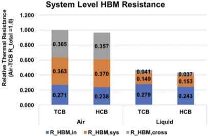
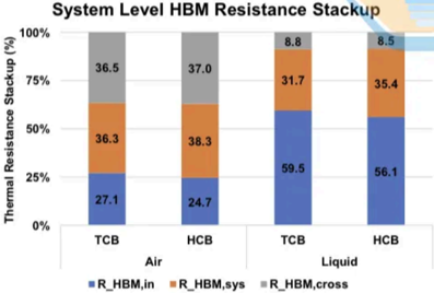
Samsung HBM thermal resistance with TCB and HCB under air and liquid cooling. Source: Samsung, 'System-Level Thermal Validation of 2.5D Packages in GPU Servers: Impact of TCB vs HCB HBM Platforms,' ECTC 2026
Samsung compared thermal compression bonding (TCB) and hybrid copper bonding (HCB) for HBM on 2.5D GPU packages with 2 GPU dies and 8 HBM stacks, similar to Nvidia Blackwell. The internal HBM thermal resistance drops by 12.2% with air cooling and 12.9% with liquid cooling. Total HBM thermal resistance drops by 3.5% with air cooling and 7.7% with liquid cooling.
The improvement is uneven as HCB only addresses part of the thermal network. Samsung separates the path into internal resistance, system-level resistance, and GPU-to-HBM crosstalk. The internal resistance and crosstalk drop by ~12.5% and ~9.8% respectively, but the system-level resistance, including thermal interface materials and cooling, increases by ~2.3%.
37.0
1.2
1.1
1|
IEEE
HCB Advantage Grows in Memory-Driven Era
=ГО PACKAGING
ELECTRONICS
SOCIETY
ECTC
The 2026 HEL 76t8 Electronic Ca
• Thermal resistance gap widens as HBM base die power scales (x1 → x3)
• GPU-to-HBM crosstalk decreases — stack resistance becomes the dominant
- constraint
1.3
- Base Die Power Sweep Thermal Crosstalk 2 4R cross =2.6
Relative Thermal Resistance
0.9
x1
SAMSUNG
- R_HBM_TCB
R_HBM_HCB
TCB-HCB
AR=7.6
-
GPU to HBM, TCB
-
GPU to HBM, HCB
4R cross =2.4
1 -
AR cross =10.2
x1
2026 IEEE 76th Electronic Components and Technology Conference | Orlando, Florida | May 26 - May 29, 2026
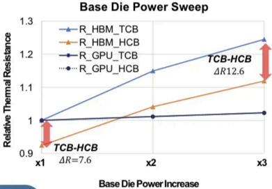
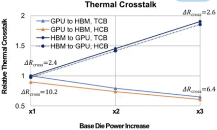
HBM thermal resistance as base die power increases. Source: Samsung, 'System-Level Thermal Validation of 2.5D Packages in GPU Servers: Impact of TCB vs HCB HBM Platforms,' ECTC 2026
As more power moves into the HBM base die, such as in memory-bound workloads, the thermal bottleneck shifts. This is especially relevant for custom HBM, where the memory controller and more logic move into the base die. GPU-to-HBM crosstalk becomes a smaller share of the total thermal resistance, falling from 13% at 1× base-die power to 5% at 3× base-die power.
According to Samsung, moving to HCB could allow for higher inlet temperatures or higher package power. In its estimate, moving to HCB allows inlet temperatures to rise by 1-2 °C at constant package power, or package power to increase by ~4% at constant temperature. Samsung also estimates cooling power would fall by ~7%.
Stack thermal resistance
[Normalized]
1.1
Stack-level thermal resistance with TCB and HCB with varying pad density (P.D.) in HCB. Source: Samsung, 'System-Level Thermal Characterization of Hybrid Cu Bonded HBM on 2.5D Advanced Packaging,' ECTC 2026
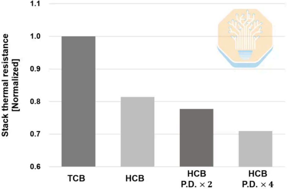
Samsung also isolated the impact of HCB at the stack level. The improvement is much larger here: Baseline HCB reduces stack thermal resistance by ~19% versus TCB. Increasing the HCB pad count raises the reduction to 22.3% at 2× pad density and 29.1% at 4× pad density.
Microfluidic Cooling
R1
R4
R11
R14
J:HBM heater group
:SoC thermal sensor
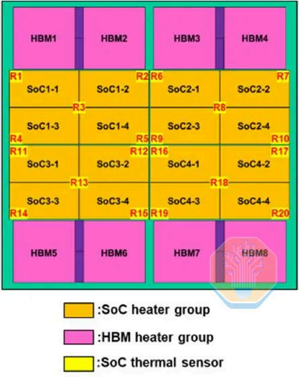
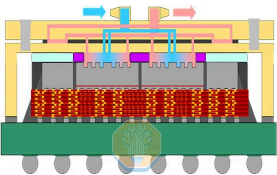
Direct-to-silicon cooling concept and CoWoS-R test vehicle. Source: TSMC, 'Process Development and Thermal Characterization of Micropillar Direct-to-Silicon Liquid Cooling Solution on CoWoS-R Platform,' ECTC 2026
TSMC showed direct-to-silicon cooling on a large GPU-like test vehicle on CoWoS-R. CoWoS-R differs from CoWoS-S by using an organic rather than a silicon interposer. CoWoS-R was chosen as it provides better warpage tolerance and process compatibility. The test vehicle uses a 3.3× reticle interposer with 4 SoC dies and 8 HBM stacks. Each
SoC die consists of 4 SoC heater groups, which together cover roughly half the interposer area.
Micropillar
Micropillar
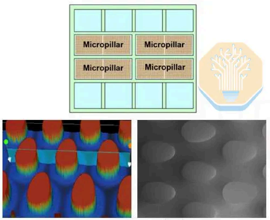
Silicon micropillar formation on the backside of the SoC dies for heat dissipation. Source: TSMC, 'Process Development and Thermal Characterization of Micropillar Direct-to-Silicon Liquid Cooling Solution on CoWoS-R Platform,' ECTC 2026
TSMC compared three approaches: a conventional lidded cold plate package, a lidless cold plate package, and its micropillar direct-to-silicon design. The lidded and lidless cases still use traditional cold plates and thermal interface material (TIM). For the last variant, micropillars were formed directly onto the backside of the SoC dies.
Thermal Design Power (kW)
1.0
0.0
0
Thermal characterization of test vehicle with and without lid, and with micropillars. Source: TSMC, 'Process Development and Thermal Characterization of Micropillar Direct-to-Silicon Liquid Cooling Solution on CoWoS-R Platform,' ECTC 2026
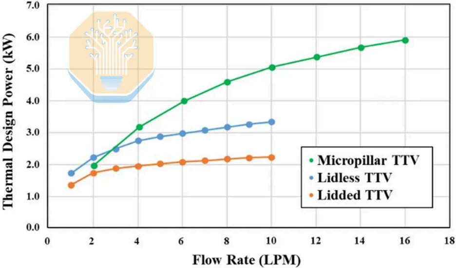
With conventional cooling at 1-2 liters per minute (LPM), a lidded package dissipated 1.92.3 kW while the lidless package dissipated 2.5-3.0 kW, using relatively warm 40 °C DI water. Both solutions saturate beyond 4 LPM because TIM becomes the bottleneck.
The micropillar test vehicle matched the lidless cold plate result at 2 LPM, then pulled ahead at higher flow rates, dissipating 4 kW at 4 LPM and 5.3 kW at 8 LPM. Across the full test vehicle, TSMC reported uniform power dissipation above 5 kW. The micropillars brought the liquid coolant into much closer proximity to the heat source, facilitating this improvement.
However, micropillars are not without downsides. TSMC had to form the micropillars after chip-on-wafer (CoW) processing without damaging the CoWoS-R structure and develop new sealant materials to keep the coolant contained despite package warpage and thermal expansion mismatch. The test vehicle passed moisture sensitivity level 4 (MSL4) with no helium leakage or sealant delamination.
Unfortunately, this was one of only 3 papers by TSMC at ECTC as compared with Intel's 12 and Samsung's 11.
(a)
0.70
Inlet
Outlet
• Package •GPU • HBM
Microsoft's direct-to-silicon microfluidic cooling assembly for Nvidia GH200. Source: Microsoft, 'Direct to Silicon Microfluidic Cooling for Datacenters,' ECTC 2026
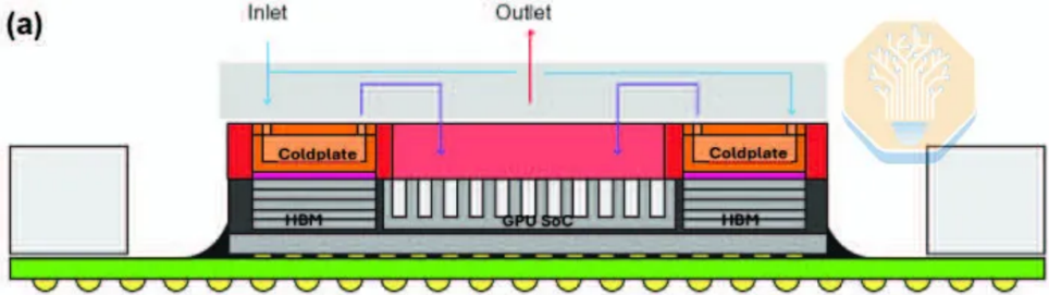
Microsoft's approach differs from TSMC's in the cooling structure. While TSMC used silicon micropillars, Microsoft used straight microchannels etched into the GPU silicon. Instead of using a thermal test vehicle, Microsoft tested on an actual Nvidia GH200 GPU. This likely allowed Microsoft to capture real thermal distribution and hotspots more accurately. Microsoft tested a variety of workloads on the GPU such as HPCG and HPL, each with different compute and memory stress characteristics.
Microsoft GH200 microfluidic cooling results across GPU workloads. Source: Microsoft, 'Direct to Silicon Microfluidic Cooling for Datacenters,' ECTC 2026
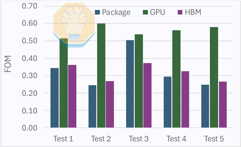
Across these workloads, Microsoft reports 51-60% lower junction-to-inlet thermal resistance for the GPU at a 1 LPM flow rate. The HBM improved less, at only 27-37%, because it was still cooled through a cold plate and TIM. Overall, this results in a 50% reduction in thermal resistance for the package.
Driver / TIA
WDM
(MUX/DeMUX)
FAU
Microsoft also showed some preliminary reliability data. While thermal performance is important, datacenter deployments also require high reliability and low downtime. Over a period of 6 months, Microsoft recorded only 9 potential clogging events across ~4370 observations. The rate declined over time, suggesting early instability after installation, followed by a more stable operating period. Even after 6 months, there was no measurable silicon erosion in the microchannels. At the node level, the GH200 successfully completed 3 weeks of repeated benchmarking followed by a 1-week continuous run at a stable package power. Microsoft is still testing cluster-level mean time between failures (MTBF) and availability. Electronic IC (EIC)
Marvell Optical Interconnects
Another prevalent theme at ECTC was optical interconnects and co-packaged optics. Marvell had several papers in this area, primarily on its Optical Multi-Chip Interconnect Bridge (OMIB) and Photonic Fabric, both of which it acquired through its purchase of Celestial AI earlier this year.
While photonic interposers have been discussed for a few years, Marvell showed off a more localized version at ECTC. Fabricating a multi-reticle photonic interposer will likely prove challenging for yields, especially due to reticle stitching. Marvell also noted that a photonic interposer may lack features available in conventional silicon interposers such as high-density capacitors.
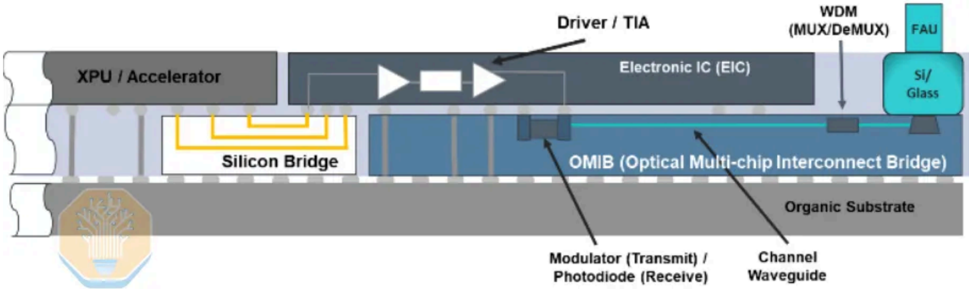
OMIB package concept with EIC stacked on PIC and an electrical bridge embedded in an organic interposer. Source: Marvell, 'Optical Multi-Chip Interconnect Bridge (OMIB) Interposer Demonstration to Enable High-density Photonic Interconnects for High-Performance Computing Applications,' ECTC 2026
Marvell's approach has a photonic integrated circuit (PIC) embedded in the organic RDL interposer only where it is needed. In other regions where optical interconnects are not required, an electrical bridge can be used instead.
As the PIC is embedded in the RDL, its grating couplers would normally be obstructed after overmolding. Marvell places a silicon/glass optical block over the grating region
before molding to maintain an optical path to the top, where the fiber array unit (FAU) can be attached.
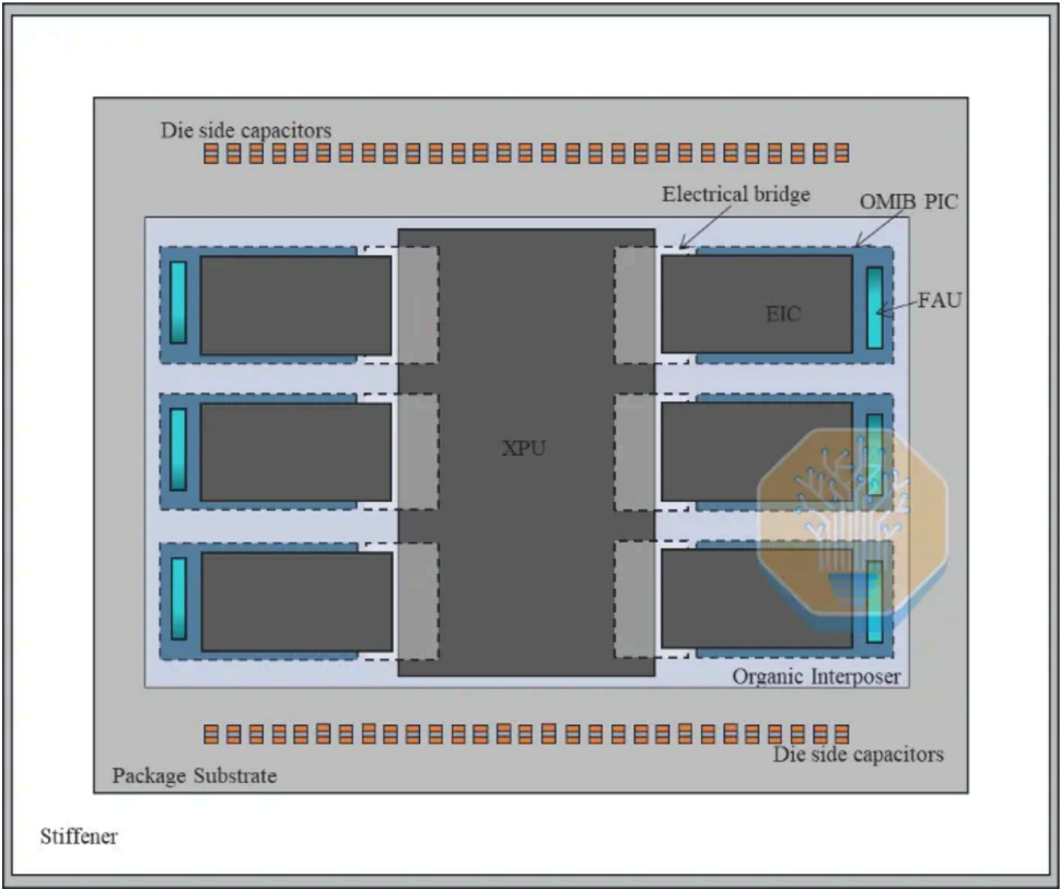
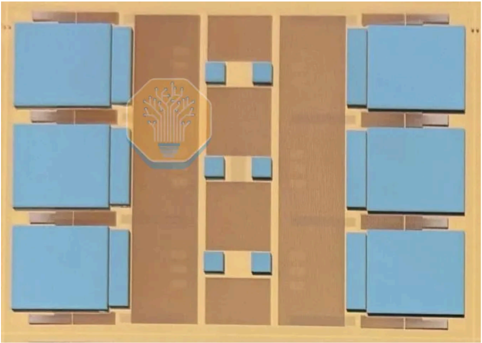
OMIB test vehicle floorplan and RDL interposer after PIC, electrical bridge, and DTC attach. Source: Marvell, 'Optical Multi-Chip Interconnect Bridge (OMIB) Interposer Demonstration to Enable Highdensity Photonic Interconnects for High-Performance Computing Applications,' ECTC 2026
e
Marvell's OMIB test vehicle has one primary XPU die and six EIC dies on top. Embedded in the interposer are six PICs (big blue rectangles), six electrical bridges (thin blue rectangles) and 12 DTC dies (small blue squares). The roughly 2×-reticle RDL interposer uses four layers at 2/2 µm L/S.
HBM
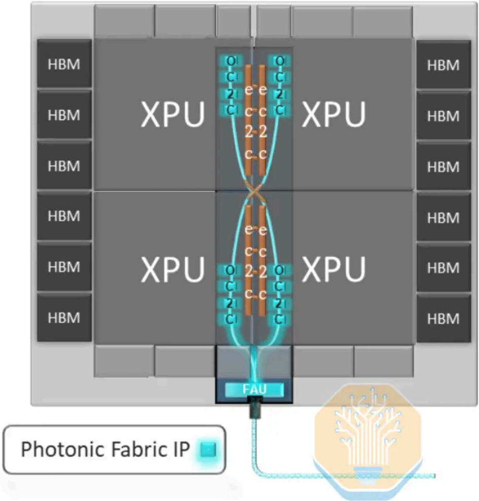
Concept of OMIB with XPU-XPU interconnect and external FAU. Source: Marvell, 'Optical Multi-Chip Interconnect Bridge (OMIB) Interposer Demonstration to Enable High-density Photonic Interconnects for High-Performance Computing Applications,' ECTC 2026
Marvell also showed off a conceptual multi-die XPU with optical chip-to-chip interconnects to reduce latency and hop count. Marvell claims that OMIB removes the shoreline
'V
*3
*H
limitations, since the same bridge can route both on-package die-to-die links and external optical interconnects. Marvell cites a bandwidth density of 1.8 Tbps/mm² with this approach. 'T
Process flow of 2.5D OMIB integration. Source: Marvell, 'Optical Multi-Chip Interconnect Bridge (OMIB) Interposer Demonstration to Enable High-density Photonic Interconnects for High-Performance Computing Applications,' ECTC 2026
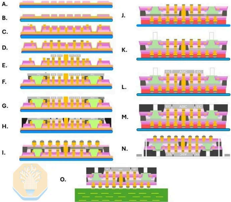
The process flow shown by Marvell is chip-last, similar to TSMC's CoWoS-L. Marvell builds an organic RDL interposer with embedded bridges, OMIB PICs, DTCs, and other components, with C4 bumps connecting it to the package substrate. Bridge TSVs and tall copper pillars connect to the RDL, and the ASIC dies and EICs are attached last.
Si-Interposer
Silicon Bridge
Router
Driver / TIA
WDM
(MUX/DeMUX)
FAU
Package concepts with optical engine on substrate, OMIB and photonic interposer. Source: Marvell, 'Photonic Fabric™ Interconnect for a Scale-up Network Solution in Accelerated Computing,' ECTC 2026
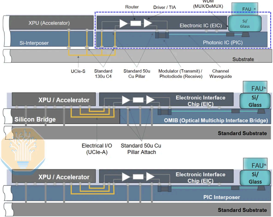
In the near term, vertically stacked optical engines like TSMC's COUPE are more achievable than OMIB-style connections or a full photonic interposer. Marvell connects the EIC and PIC using microbumps at 50 µm pitch, then mounts the resulting engine to either the package substrate or an interposer.
The substrate configuration can use a UCIe-S-like parallel bus at a coarse 130 µm C4 pitch, while the interposer configuration can use a UCIe-A interface at a tighter ~40-45 µm pitch. Marvell favors the substrate approach due to its simplicity and better thermal isolation.
RX0
510 um
RX1
Photonic Fabric optical link test chip EIC with four TX-RX pairs. Source: Marvell, 'Photonic Fabric™ Interconnect for a Scale-up Network Solution in Accelerated Computing,' ECTC 2026
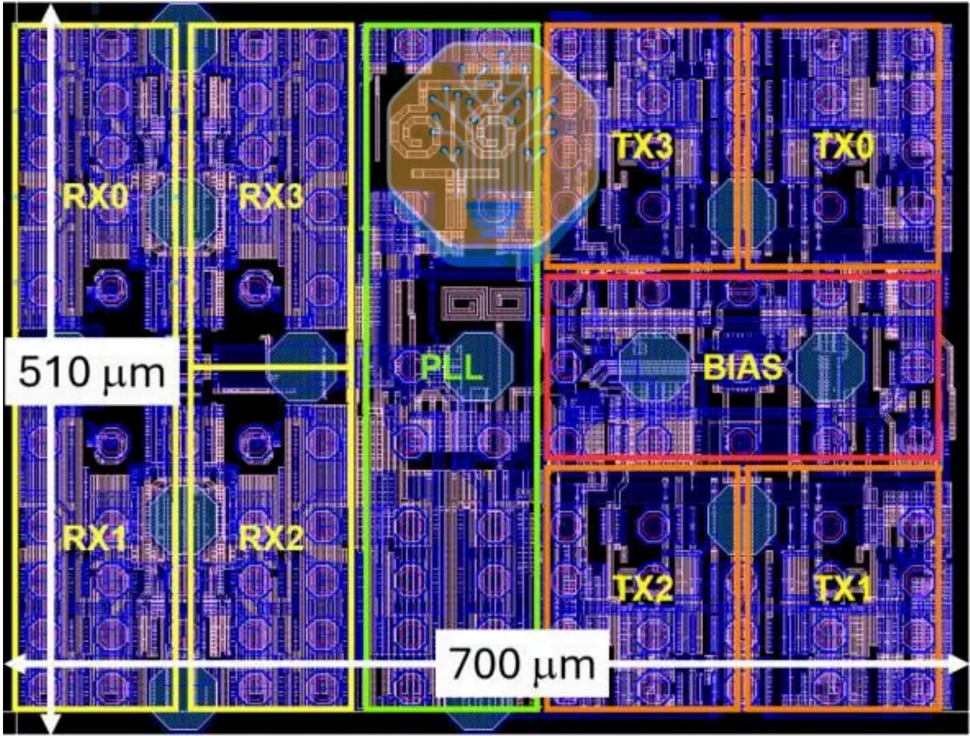
Marvell tested an optical engine using a 5 nm (likely TSMC N5) EIC, with four 56 Gb/s TXRX pairs for 224 Gb/s in each direction. The design uses electro-absorption modulators (EAMs) instead of the micro-ring modulators (MRMs) preferred by other companies, citing better thermal stability and a wider operating wavelength range. While these advantages are real, we believe that EAMs will prove difficult to manufacture at scale.
100.0
-
93.5
-
87.0
80.5
• 74.0
- 67.5
61.0
- 54.5
48.0
• 41.5
35.0
Cold Plate
EIC
PIC steady-state temperature gradient under full XPU power on substrate, silicon interposer and silicon bridge. Source: Marvell, 'Photonic Fabric™ Chiplets for Co-Packaged Optics in AI Data Centers,' ECTC 2026
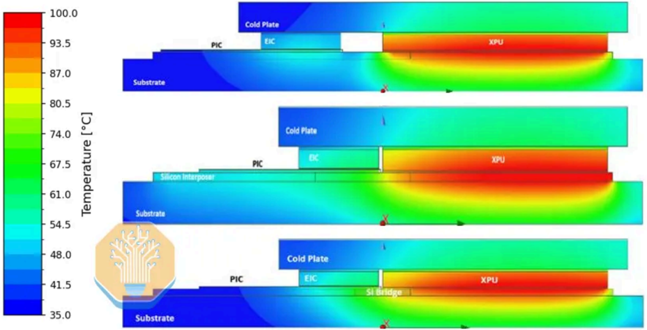
Marvell also compared the thermal characteristics of an optical engine connected via UCIe-S on substrate and UCIe-A both on a silicon interposer and over a silicon bridge. Under full XPU load, the PIC temperature rose by less than 5 °C on the substrate, versus ~25 °C on the interposer and ~20 °C with the bridge. The organic substrate's low thermal conductivity and relatively large millimeter-scale air gap isolate the PIC. In both UCIe-A configurations, the fine-pitch silicon close to the XPU provides a low-resistance thermal path. There is also a much smaller air gap, at only ~100 µm, which contributes to the heating of the PIC.
PIC
XPU
Temperature Rise AT (°C)
PIC transient temperature rise on substrate, silicon interposer and silicon bridge. Source: Marvell, 'Photonic Fabric™ Chiplets for Co-Packaged Optics in AI Data Centers,' ECTC 2026
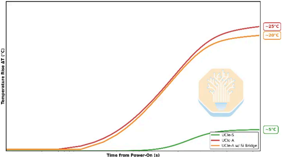
The thermal transients occur within ~30 ms of an XPU power-state change. The PIC heats at ~10 °C/s on the organic substrate, versus ~100 °C/s with the bridge and ~120 °C/s on the interposer. Marvell argues that the EAM bias voltage can be adjusted electronically fast enough to track these changes, while ring modulators require heater-and-feedback loops, which are constrained by slower time constants.
Lightmatter Passage M1000
Lightmatter has previously detailed the Passage M1000's architecture and optical interconnects, and has outlined its manufacturing approach. At ECTC, it provided a much deeper look at the assembly process, fiber attachment, and packaging results for integrating the multi-reticle photonic interposer with ASIC chiplets.
ASIC top die chiplets
Passage
Passage M1000 schematic. Source: Lightmatter, 'Advancing Interconnect Performance and Reliability with Innovations in 3D Photonic Integration Packaging and Fiber Coupling,' ECTC 2026
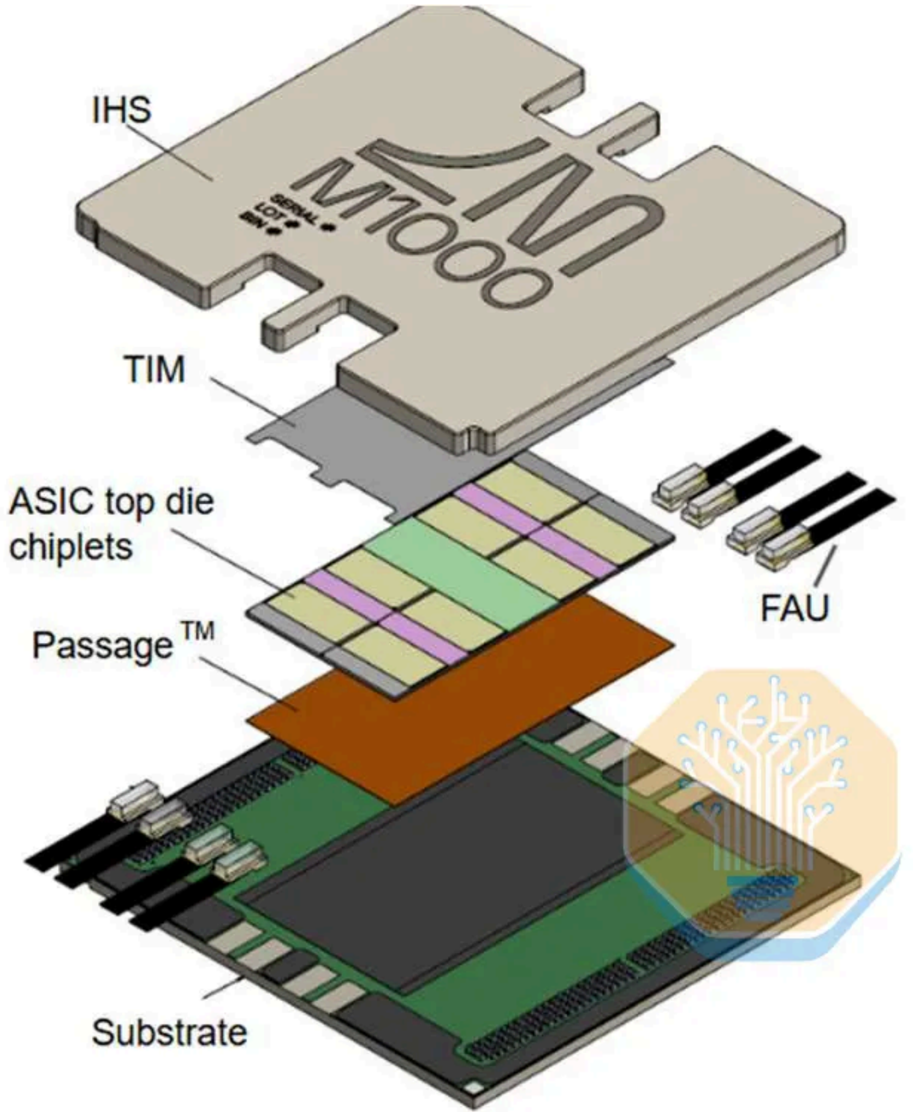
The test vehicle uses chip-on-wafer assembly to attach 15 ASIC chiplets to a four-tile M1000 interposer. We estimate the interposer measures ~2100 mm², about half of the 4000 mm² eight-tile configuration shown at Hot Chips 2025. The M1000 is highly configurable to different sizes and tile counts depending on the needs of the product.
Each of the four tiles has 32 optical waveguides at 127 µm pitch. Electrical signals and power travel from the substrate to the ASIC chips through the C4 bumps at ~176 µm pitch, two backside RDL layers, and 126 µm deep TSVs with a 10 µm width before reaching the
5
40-4
5 20 4
200
50 -
200
Room temp
25 °C
45.6 um
100 °C
32.1 um
200 °C
17.8 um
ASIC chiplets through microbumps. The ~2100 mm² interposer occupies less than onethird of the 7200 mm² organic substrate. This ratio is closer to the logic area to package size ratio than the package-spanning interposer area of an equivalent silicon or organic RDL solution. It is unclear whether this is a consequence of the optical architecture or a design choice specific to this test vehicle. man 40 20 100 100 00 20 40
Reflow temp
150
Cool down
Cool down
Passage M1000 package warpage during temperature ramp-up and cool-down. Source: Lightmatter, 'Advancing Interconnect Performance and Reliability with Innovations in 3D Photonic Integration Packaging and Fiber Coupling,' ECTC 2026
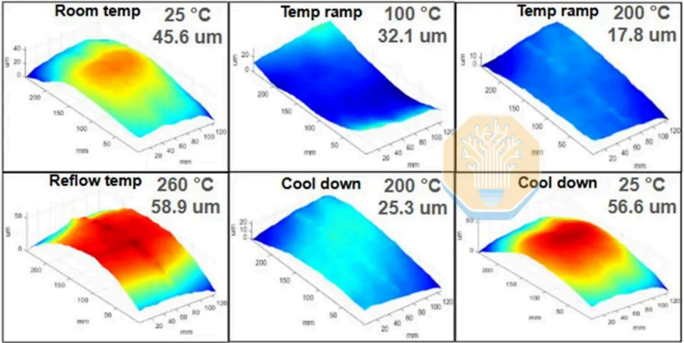
Attaching a silicon interposer of this size to an organic substrate creates severe warpage. The module reached ~59 µm of warpage at the 260 °C reflow temperature, and ~56 µm after cooling back down to room temperature. With a 118 µm-thick interposer and C4 bumps at ~176 µm pitch, this is enough to compromise joint formation. Lightmatter used a magnetic fixture to hold the substrate flat during attachment and reported >95% electrical assembly yield, with healthy microbump and C4 joints across the package.
260 °C
200 °C
25 °C
Temp ramp
Temp ramp
M O
29.3*
20
Thermal map of the test chip at 170 W per quadrant. Source: Lightmatter, 'Advancing Interconnect Performance and Reliability with Innovations in 3D Photonic Integration Packaging and Fiber Coupling,' ECTC 2026
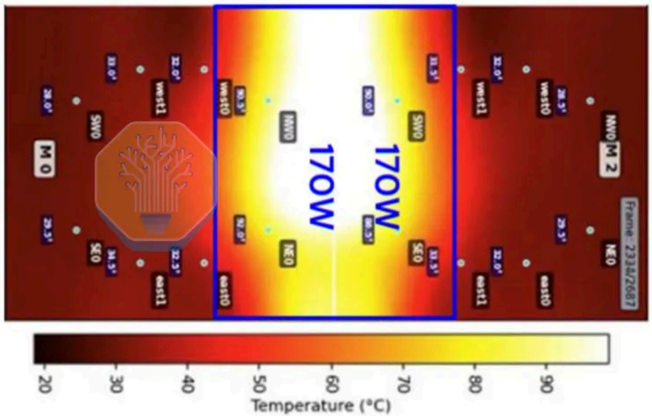
Lightmatter used a thermal test chip with four independently powered quadrants, each dissipating 170 W. This resulted in a power density of 1.47 W/mm² across the 369 mm² active area. At this power, the photonic interposer reached approximately 100 °C using a 25 °C coolant flowing at 1.8 LPM/kW. This validates cooling 680 W from a concentrated test-chip area in a package designed for more than 900 W across nearly three reticles of ASIC silicon.
Other Highlights
Hybrid Bonding
Hybrid copper bonding still delivers the finest pitch and highest I/O density for HPC applications. The open problem is keeping the interface extremely flat and clean while reducing the bonding temperature. Two material approaches stood out this year.
The first uses organic dielectrics, whose mechanical compliance increases tolerance to particles and surface roughness while reducing bonding stress. Mitsui Chemicals and ASE demonstrated pressure-less Cu/polymer bonding at 200 °C and 10 µm pitch. TOK and NYCU demonstrated a 10-second bonding process at 150 °C. Samples bonded at 200 °C maintained stable resistance through reliability testing.
a) FG-Cu_vl b) FG-Cu_v2
Void-free C-SAM bonding maps for fine-grain Cu annealed at 175 °C and 200 °C. Source: Intel, 'Enabling Ultra Low Temperature Hybrid Bonding for D2W Scaling,' ECTC 2026
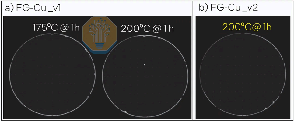
The second approach uses fine-grain copper. Its higher grain-boundary density accelerates copper diffusion at lower temperatures, and subsequent grain growth increases conductivity. Intel combined fine-grain copper with a low-temperature dielectric stack, achieving uniform wafer bonding after 175 °C and 200 °C anneals. Electrical yield was around 60% in two of three samples, although Intel described these results as a lower bound due to test vehicle and probing limitations. The experiments used wafer-to-wafer (W2W) test vehicles rather than the die-to-wafer (D2W) process targeted by the technology.
The most aggressive pitch came from Applied Materials and EV Group, which demonstrated 450 nm pitch wafer-to-wafer bonding at 98% yield across a chain of 20 million links. Failure analysis associated open links with carbon-rich benzotriazole (BTA) residue at the copper interface. A PVD TaN/Ta barrier stack significantly improved yield. CEA-Leti separately achieved greater than 97% yield after a 100 °C anneal without plasma activation.
Together, these results show that reducing pitch and bonding temperature requires the copper, dielectric, CMP, surface preparation, and annealing to be co-optimized to achieve hybrid bonding with low warpage and no cracking. We expect continued refinement by material suppliers and equipment vendors to improve post-bond yield from 2027 onward.
Interposer Alternatives
As package sizes outgrow the practical limits of circular silicon interposers, more vendors are proposing interposer-less integration schemes beyond Intel's EMIB-T.
Top die SOC
Microbumps -
Embedded memory chiplet
SoC
Schematic cross-section of FO-EB with embedded memory chiplet. Source: Intel and SPIL, '3D Integration of an SRAM chiplet in Fan-Out Embedded Bridge Platform Achieving Low Energy Read/Write,' ECTC 2026
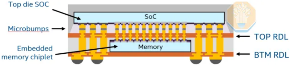
Intel and SPIL placed an SRAM chiplet in the embedded-bridge layer of a fan-out embedded bridge (FO-EB) package, connecting it vertically to the logic die through 25 µm pitch microbumps. The test chip reached more than 265 GB/s/mm² at 0.24 pJ/b.
Panel-scale organic interposers provide another route around the size limits of silicon. Resonac demonstrated the individual process modules for a dry-film embedded-bridge interposer on a 320 mm × 320 mm panel, including 5 µm microvias and 2/2 µm L/S. ASE fabricated an RDL on a 600 mm × 600 mm panel, then divided it into four 300 mm × 300 mm panels for assembly with existing equipment. Its test vehicle used three RDL layers at 5/8 µm L/S.
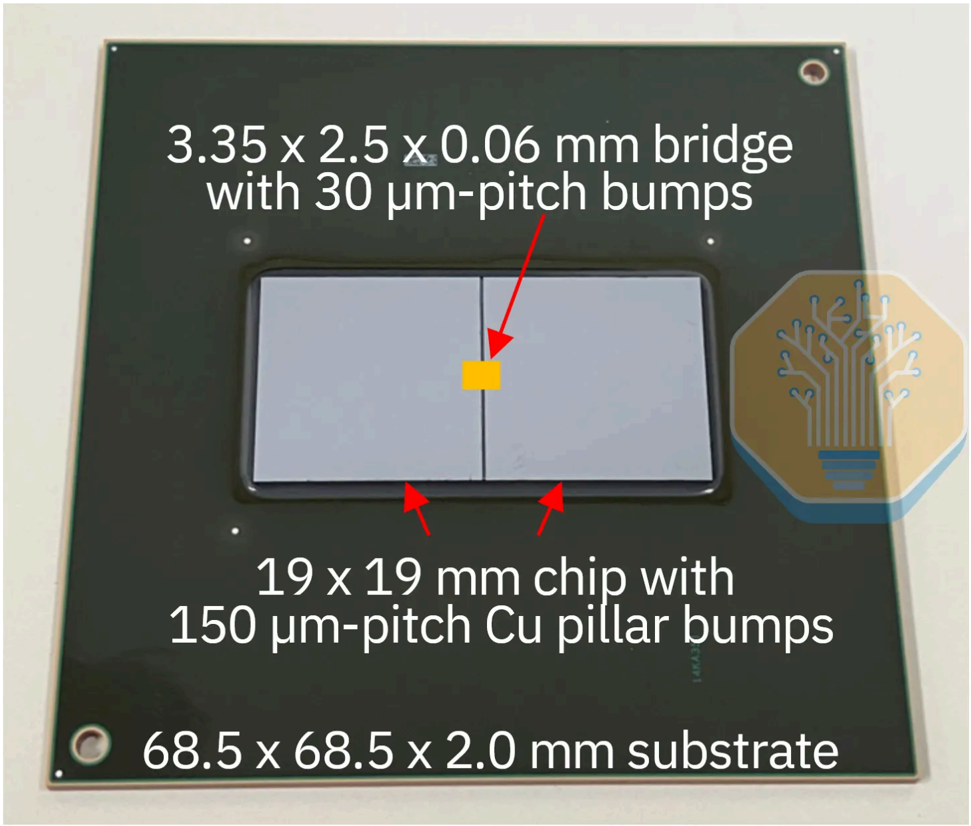
Direct Bridge Multi-die with a 30 µm pitch silicon bridge. Source: IBM, 'Direct Bridge Multi-die (DBrM) Package: A Novel Silicon Bridge Chiplet Packaging Technology Using Die-Edge Gluing Technique for Chip Reconstitution,' ECTC 2026
IBM took a more localized approach with Direct Bridge Multi-die (DBrM). Chiplets are first joined along their edges, creating a mechanically rigid subassembly around a 30 µm pitch silicon bridge. The subassembly withstood more than 30 N in bending tests, versus 0.2 N for IBM's previous underfill-only structure. This is a positive result for reducing warpage.
Silicon Bridges for Chiplets
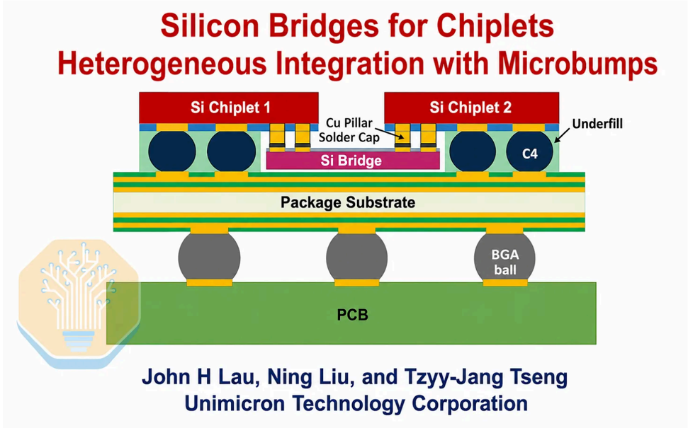
Chiplets connected through a silicon bridge without an interposer. Source: Unimicron, 'Silicon Bridges for Chiplets Heterogeneous Integration with Microbumps,' ECTC 2026
Unimicron modeled an even simpler structure requiring neither an interposer nor embedded bridges. Two chiplets connect through a thin silicon bridge mounted beneath them while attaching directly to the substrate. Unimicron's simulations show that underfill between the chiplets and bridge is necessary to control microbump strain.
While TSMC's CoWoS-R and CoWoS-L remain limited by the circular wafer on which their RDLs are fabricated, constraining package size and wafer utilization, these alternatives shift integration to panel-level or reconstituted formats or eliminate the interposer entirely. We expect similar architectures to begin appearing in ASICs over the next several years.
Thermal Interface Materials
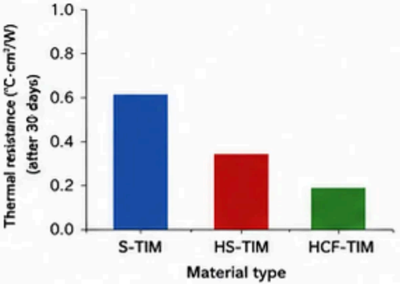
In advanced thermal solutions, TSMC and its partners continue to dominate the show. TSMC's direct-to-silicon cooling removes TIM1 entirely, but most near-term systems will still need better materials between the silicon and heat spreader. TSMC's OSAT partner, SPIL, tested gallium-based liquid-metal (LM) composites, a silicone-based HS-TIM and a carbon fiber HCF-TIM, in a 55 mm × 55 mm FO-EB package. Their measured conductivities were 5.7 W/m·K and 10 W/m·K respectively, and both produced lower thermal resistance than a commercial silicone TIM at 4 W/m·K.
Material
Filler type
Thermal conductivity
Properties of selected TIMs
Traditional S-TIM
HS-TIM
LM alloys
HCF-TIM
LM alloys
| Al + ZnO | + Al,03 | + Carbon fiber |
|---|---|---|
| 4 W/mK | 5.7 W/mK | 10 W/mK |
Both HS-TIM & HCF-TIM showed lower thermal resistance and more stable performance. 1.0
Thermal resistance (*C-cm'/W)
(atter 30 days)
Thermal performance and reliability of liquid-metal HS-TIM and HCF-TIM. Source: SPIL, 'Reliability Assessment of Liquid Metal Alloy Thermal Interface Materials in Fan-Out Embedded Bridge (FO-EB) Packages,' ECTC 2026
The two TIMs exhibited drastically different reliability outcomes, with HCF-TIM maintaining 95% coverage after 1000 hours at 150 °C while HS-TIM fell to only 75% as its silicone matrix hardened and partially delaminated. Both LM-based TIMs reduced thermal resistance relative to conventional S-TIM, with HCF-TIM delivering the best performance and reliability.
Purdue, the University of Aveiro, and UCLA took a different approach, embedding Cu/Sn microbumps in nanocrystalline diamond. The resulting interconnect layer reached an effective in-plane thermal conductivity of 500 to 600 W/m·K, around twenty times that of conventional microbumps with underfill. This is not a TIM1 replacement, but a way to spread heat laterally through the interconnect layer of a 3D stack. The process remains early, with the paper only using a single-sided test structure rather than an assembled 3D stack.
On the other hand, we saw little discussion on SiC as TIM1 or part of thermal solutions, implying a relatively long way till maturity.
Glass Substrates
Glass's aurora dimmed somewhat this year, with fewer innovative papers presented at ECTC. However, the unsolved problem is still SeWaRe, the lateral crack that begins at a diced glass edge under RDL stress. Georgia Tech characterized the failure experimentally. Corning used finite element analysis (FEA), peridynamics, and analytical fracture mechanics to model its propagation, showing that stiff copper layers drove cracks towards the glass midplane, while compliant polymer layers changed the crack path. Corning also found that low-CTE polymers combined with appropriate glass selection could reduce the failure risk.
PKG
Die
Memory
Substrate
Category
Items
Organic TV
Glass TV
| Configuration | ||
|---|---|---|
| Size | 74x74mm 73.4x73.4mm/ 2.5mmT | 74x74mm 73.4x73.4mm/ 2.5mmT |
| Size ERDa | 25x25mm (X2) 130um | 25x25mm (X2) 130um |
| Layer # | 0.4mm 14L(6-2-6) 8L(3-2-3) | 0.4mm 14L(6-2-6) 8L(3-2-3) |
| Core / Thickness PTH/TGV Size ABF Material | E705G / 1.2mm 150um Glass / 0.6mm | 90um GL102 |
| Thickness | 1.81 mm | |
| 0.92mm | 0.92mm |
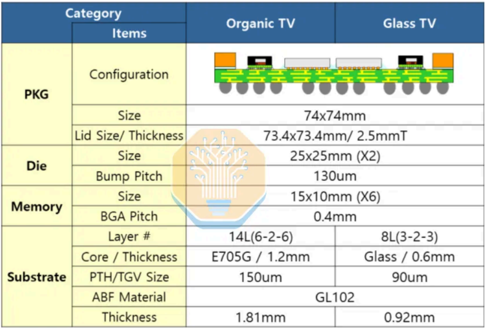
Comparison of the 74 × 74 mm organic- and glass-core test vehicles. Source: STATS ChipPAC,
'Assembly and Reliability Characterization of Glass-Cored Substrate Package for AI/HPC Applications,' ECTC 2026
STATS ChipPAC investigated the assembly and reliability of large glass-core packages. Its 74 mm × 74 mm glass-core packages failed every test segment without edge coating, while the edge-coated packages completed assembly and reliability testing without abnormalities. The edge coating also reduced warpage by 33.5% relative to the uncoated glass-core package. Build-up pull-back and edge coating increasingly look like requirements for reliable glass-core substrate assembly.
24-layer (10-2-10) glass-core panel with copper-filled TGVs, embedded EMIB bridges and optical waveguides, with singulated units showing no SeWaRe after thermal-shock testing. Source: Intel, 'Glass Core Substrates - Next Generation Advanced Packaging Platform for AI and HPC,' ECTC 2026
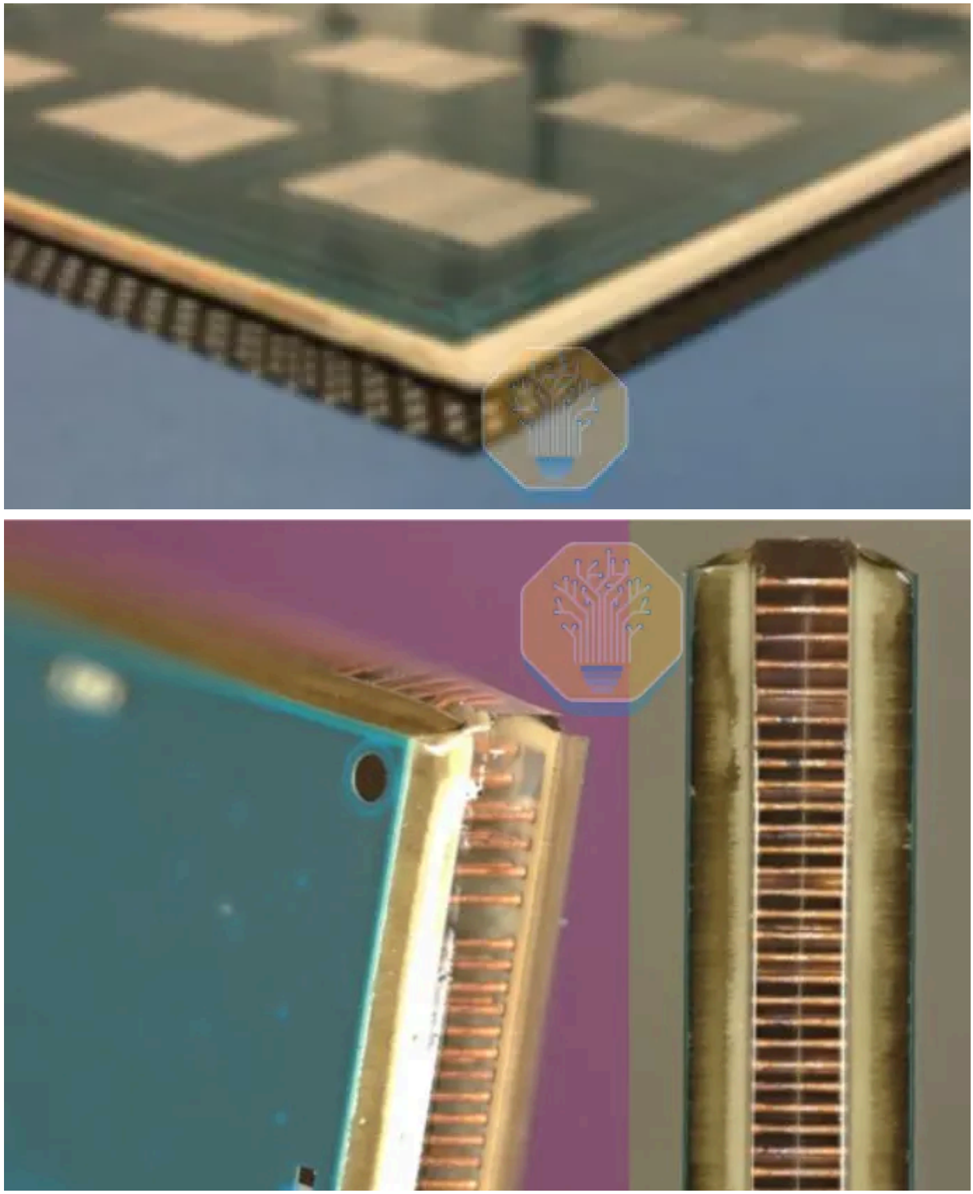
On a positive note, Intel demonstrated an industry-first 510 mm × 515 mm, 24-layer glasscore panel with fully copper-filled through-glass vias (TGVs), two embedded EMIB bridges, and optical waveguides co-formed between the TGVs. The large prototype was displayed at Intel's booth. It was processed on existing organic-substrate lines, while singulated units showed no SeWaRe after thermal shock testing.
As OSAT adopters, Amkor and STATS ChipPAC measured 30-40% lower substrate-level warpage with a thinner glass core than their organic references, although assembly defects and TGV filling problems show that the process remains immature.
Glass is making real progress, but this year's data still support manufacturing development rather than high-volume adoption.
RDL Scaling
Finally, RDL L/S continues to shrink even as package sizes grow. The primary driver is UCIe 3.0, which supports speeds of up to 64 GT/s for future ASIC-to-ASIC and ASIC-toHBM links. These high-speed die-to-die interconnects tighten signal integrity requirements as organic interposers grow larger and denser.
The roadmap has progressed from 10/10 µm line/space around 2015 to 2/2 µm today, with 1/1 µm emerging as the next target. Reaching the submicron era will require major changes to both RDL routing architectures and manufacturing processes. The process is shifting from semi-additive plating towards damascene for sub-2 µm copper, where CMP planarization and low-shrinkage dielectrics become the key gating steps.
Resonac used polymer damascene and panel CMP to form 2/2 µm wiring on a 320 mm × 320 mm glass panel, including a four-layer via-and-trench structure. imec and Fujifilm pushed damascene to 1/1 µm on 300 mm wafers. Ushio resolved 1.5/1.5 µm L/S over an 18-reticle field without stitching, with 16 exposures covering a full 510 mm × 515 mm panel. Sumitomo Bakelite and Georgia Tech showed a fully imidized liquid dielectric with only 4% cure shrinkage at a relatively low temperature of 200 °C and a fine 2/2 µm L/S.
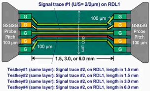
- UCle-A IP & CoWoW-R Silicon Correlation
This work correlates at two silicon measured approaches, which are (1) high speed interconnect test keys in S-Param. by VNA; (2) 16 & 32
G
G
GT/s eyediagrams on an evaluation board environment by oscilloscope. Signal trace #1 (U/S= 2/2um) on RDL1 100 pm G TABLE I. S-PARAMETERS CORRELATION OF COWOS-R INTERCONNECTS TESTKEYS
GSGSG
Probe
Pitch
100 pm
G
100 um
Testkey#1 (same layer): Signal trace #2, on RDL1, length in 1.5 mm
Testkey#2 (same layer): Signal trace #2, on RDL1, length in 1.5 mm
Testkey#3 (same layer): Signal trace #2, on RDL1, length in 3.0 mm
Testkey#4 (same layer): Signal trace #2, on RDL1, length in 6.0 mm
Fig. 6. UCle-A interconnect test keys design & correlation.
GSGSG
Probe
On-board mea. EyeWidth 0.82UI
Testkey#1
Sim
Mea
Testkey#2 Sim Mea Testkey#3 Sim Mea Testkey#4 Sim Mea
S:2/2
G:5/2
1.50
1.75
14.9
Design
Index
L/S
(um)
Length
(mm)
IL (dB)
RL (dB)
| S:2/2 | S:2/2 | S:2/2 | S:2/2 | S:2/2 | |
|---|---|---|---|---|---|
| G:5/2 | G:4/2 | G:4/2 | |||
| 1.50 1.50 | 1.50 3.00 | 3.00 | 3.00 | 6.00 6.00 | 6.00 6.00 |
| 2.06 2.03 | 2.05 | 2.82 2.67 | 5.84 | 5.90 | |
| 13.2 11.8 | 11.5 | 20.3 20.8 | 14.9 | 12.5 | |
| -40.9| -41.3 | -41.6 -35.0 | -37.7 | -41.3 | • -41.6 |
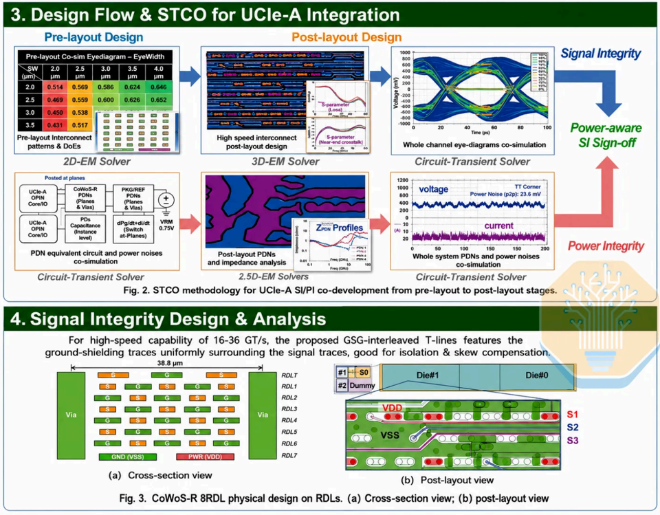
Design flow and STCO for UCIe-A on 8-layer CoWoS-R RDL. Source: GUC, 'Design of UCIe-A x64 Chiplets Integration for 16-36 GT/s Using Organic Interposer,' ECTC 2026
As the most advanced RDL manufacturer, TSMC also collaborated with GUC to present their work on 8-layer RDL scaling, which is believed to be the near-term limit of the CoWoS-R platform. GUC demonstrated an STCO-based design and validation flow for integrating a 64-bit UCIe-A interface fabricated on TSMC N3 and integrated on an 8-layer CoWoS-R RDL.
Its STCO framework uses ground-signal-ground interleaved transmission lines to control crosstalk and skew, while simulations show that C4-side IPDs provide localized decoupling and reduce voltage fluctuation at the chiplet microbumps.
- Design Flow & STCO for UCle-A Integration
Pre-layout Design um
0.514
0.469
0.450
(um)
2.0
2.5
3.0
3.5
0.431
Pre-layout Interconnect patterns & DoEs
Posted at planes
UCle-A
OPIN
Core/10
UCle-A
OPIN
Core/10
PDN equivalent circuit and power noises
Circuit-Transient Solver
Post-layout Design
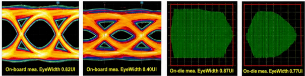
Measured UCIe-A eye diagrams at 16 and 32 GT/s. Source: GUC, 'Design of UCIe-A x64 Chiplets Integration for 16-36 GT/s Using Organic Interposer,' ECTC 2026
The design targets 16-36 GT/s with a 64-bit, 10-column UCIe-A interface at 45 µm bump pitch. Signal traces were routed at 2/2 µm across six layers, with the seventh reserved for power delivery. The test chip achieved a measured on-die eye width of 0.77 UI at 32 GT/s, while simulations showed an eye width of 0.74 UI at 36 GT/s. The results show that organic interposers can meet the signal and power integrity requirements for heterogeneous chiplet systems.
Stacked Memory
DRAM
DRAM
WiteBond
DRAM
AP
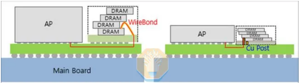
Conventional wire-bond stack versus Vertical Cu post Stack. Source: Samsung, 'Multi Stacked FOWLP utilizing Extreme Aspect Ratio Cu Post for Mobile on-Device AI Memory Solution,' ECTC 2026
Samsung showed an approach to DRAM stacking that avoids TSVs entirely. Vertical Cu post Stack (VCS) connects four stacked memory dies through <56 µm-pitch, <30 µm-wide high-aspect-ratio copper posts embedded in molding compound, rather than etching vias through silicon, while also replacing the package substrate with an RDL. Shortening the interconnect cut power consumption by 41% versus a conventional wire-bonded stack, from 0.646 W to 0.384 W at iso-speed. Samsung also reported better signaling, with maximum data rate rising from 8.6 Gb/s to 11.8 Gb/s with only 8% higher power consumption.
Cross-section of the four-high VCS DRAM stack connected by extreme-aspect-ratio copper posts. Source: Samsung, 'Multi Stacked FOWLP utilizing Extreme Aspect Ratio Cu Post for Mobile on-Device AI Memory Solution,' ECTC 2026
The form factor also improves substantially, with package height and footprint each reduced by 40% while bandwidth increases 2.6× and I/O count 6×. Although Samsung's focus is on mobile platforms like smartphones, this approach is also promising for higherpower workloads. We believe VCS and similar approaches could help future AI accelerators reach higher bandwidth at lower power and a smaller footprint, while also enabling higher-density memory modules like SOCAMMs for server CPUs.
Thanks for reading!

Recommend SemiAnalysis to your readers
Bridging the gap between the world's most important industry, semiconductors, and business.